 Yiyang Li1*†
 T. Patrick Xiao2
 Christopher H. Bennett2*
 Erik Isele1
 Armantas Melianas3Hanbo Tao1
 Matthew J. Marinella2Alberto Salleo3Elliot J. Fuller1
 A. Alec Talin1*
- 1Sandia National Laboratories, Livermore, CA, United States
- 2Sandia National Laboratories, Albuquerque, NM, United States
- 3Department of Materials Science and Engineering, Stanford University, Stanford, CA, United States
In-memory computing based on non-volatile resistive memory can significantly improve the energy efficiency of artificial neural networks. However, accurate in situ training has been challenging due to the nonlinear and stochastic switching of the resistive memory elements. One promising analog memory is the electrochemical random-access memory (ECRAM), also known as the redox transistor. Its low write currents and linear switching properties across hundreds of analog states enable accurate and massively parallel updates of a full crossbar array, which yield rapid and energy-efficient training. While simulations predict that ECRAM based neural networks achieve high training accuracy at significantly higher energy efficiency than digital implementations, these predictions have not been experimentally achieved. In this work, we train a 3 × 3 array of ECRAM devices that learns to discriminate several elementary logic gates (AND, OR, NAND). We record the evolution of the network’s synaptic weights during parallel in situ (on-line) training, with outer product updates. Due to linear and reproducible device switching characteristics, our crossbar simulations not only accurately simulate the epochs to convergence, but also quantitatively capture the evolution of weights in individual devices. The implementation of the first in situ parallel training together with strong agreement with simulation results provides a significant advance toward developing ECRAM into larger crossbar arrays for artificial neural network accelerators, which could enable orders of magnitude improvements in energy efficiency of deep neural networks.
Introduction
Machine learning and artificial neural networks have promising applications in diverse fields (Lecun et al., 2015). Such algorithms are very energy intensive to implement in conventional digital computers. The energy intensity arises from the need to shuttle large quantities of information from memory to processor to conduct large matrix multiplications and to update matrix weights (Marinella et al., 2017; Sze et al., 2017). Crossbar arrays of analog non-volatile memory elements eliminate this “memory wall” and promise to reduce the energy consumption of inference and training by conducting matrix computations locally at the memory elements (Nawrocki et al., 2016; Burr et al., 2017; Ielmini and Wong, 2018; Xia and Yang, 2019). Hardware inference accelerators for analog matrix vector multiplication, also known as dot-product engines, have been demonstrated using non-volatile memory like inorganic memristors (Yao et al., 2017; Hu et al., 2018; Li et al., 2018b; Yao P. et al., 2020; Yeon et al., 2020), organic memristors (Emelyanov et al., 2016; Lin et al., 2016; Park and Lee, 2017), phase-change memory (Ambrogio et al., 2018; Nandakumar et al., 2020; Sebastian et al., 2020), and floating gate memory (Guo et al., 2017; Lee and Lee, 2020), and may be commercialized in the coming years.
While there exist several potential hardware solutions for analog inference, in situ training accelerators based on analog memory have been extremely challenging to implement. Most analog non-volatile memory devices suffer from nonlinear and unpredictable conductance updates as well as high device-to-device variation, which reduces training accuracy (Agarwal et al., 2016). Training accelerators should also have the ability to update all weights in parallel through outer product updates to minimize latency and energy consumption (Agarwal et al., 2016; Gokmen and Vlasov, 2016). While this is achievable in very small crossbar arrays (Alibart et al., 2013), high write currents in the μA or mA preclude this ability in larger arrays due to voltage drops across the write lines. Instead, in situ training utilize sequential device-by-device weight updates (Prezioso et al., 2015; Bayat et al., 2018; Li et al., 2018a; Cai et al., 2019), resulting in extra latency and energy consumption for larger array sizes between 103 and 106 devices.
Three-terminal electrochemical random-access memory (ECRAM), also known as redox transistors, can address the accuracy, energy, and latency deficiencies of two-terminal memristors (Fuller et al., 2017, 2019b; van de Burgt et al., 2017; Sharbati et al., 2018; Tang et al., 2018; Kim et al., 2019; Li et al., 2019, 2020a,b; Melianas et al., 2020; Tuchman et al., 2020; Yao X. et al., 2020). ECRAM achieves exceptionally reproducible, linear, and symmetric weight updates by encoding information in resistance values that reflect changes in the average bulk concentration of dopants like protons in transistor-like channels. ECRAM can also achieve massively parallel weight updates: because most ECRAMs operate at room temperature and do not need joule heating for switching. The switching energy and switching current is expected to be below 1 fJ and 1 nA, respectively, for scaled devices (Fuller et al., 2017; van de Burgt et al., 2017; Sharbati et al., 2018; Li et al., 2020a). As a result, voltage drops along write lines are negligible, so all devices in the crossbar sense the same write voltage even when many devices are updated simultaneously. This enables massively parallel weight updates even when scaled to larger crossbar arrays. The ability to update all weights in parallel via an outer product is crucial for realizing analog training accelerators that substantially exceed the performance of digital ones (Fuller et al., 2019a).
While parallel weight updates have been shown using ECRAM (Fuller et al., 2019a; Kim et al., 2019), in situ training utilizing this outer product update has not been demonstrated due to overlapping fabrication and systems engineering challenges. Instead, numerical simulations (Agarwal et al., 2016; Jacobs-Gedrim et al., 2017; Bennett et al., 2019a; Kim et al., 2019) based on the switching properties of just one or few devices have been used to predict the accuracy of training large crossbar arrays (Fuller et al., 2017, 2019a; van de Burgt et al., 2017; Li et al., 2019, 2020a). Without experimental validation, it is unclear if such numerical simulations will accurately capture experimental training protocols, especially in the presence of non-ideal device behavior, variations between devices, loss of state, or sneak current pathways that are difficult to account for in array simulations using individual device measurements.
In this work, we experimentally train a small crossbar array of ECRAM cells in parallel with high efficiency alongside accuracies close to software-derived values at floating point precision. This is not only an advancement for ECRAM, but also provides the first experimental realization of scalable and parallel in situ (on-line) training utilizing outer product updates of stochastic gradient descent conducted through in-memory computing. Moreover, we also show near-perfect agreement between crossbar array simulations and experimental training results: we not only replicate the number of epochs to convergence, but also the exact evolution of conductance weight updates. This result validates these training models and provide strong evidence that ECRAM cells can accurately execute deep neural network algorithms as predicted from crossbar simulations. The highly accurate training and excellent agreement with simulation result from the linear and deterministic switching of ECRAM devices. We also consider the importance of these characteristics for both spiking and deep neural networks. By both demonstrating parallel in situ training and validating numerical simulations, we show the potential of using three-terminal ECRAMs as a platform to design in-memory hardware accelerators for efficient in situ training of artificial neural networks.
Results and Discussion
Device Fabrication and Circuit Design
We fabricate nine organic ECRAM cells using PEDOT:PSS as the mixed ionic-electronic conduction weight storage element and PVDF-HFP combined with EIM:TFSI as the ion gel electrolyte (Melianas et al., 2020). Weight updates are conducted when electrons and charge-compensating ions are moved between the gate and channel electrodes; based on past work on organic ECRAM (van de Burgt et al., 2017; Fuller et al., 2019a), we anticipate that the dominant charge-compensating ion is the proton, although it has not yet been proven for this device (Melianas et al., 2020). The weights are read using the electronic conductance of the channel. An electrochemical synapse contains an ECRAM cell paired with a fixed bias resistor, a series resistor, and two CMOS switches (MAX327CPE) as selectors (Figure 1A). The conductance of the ECRAM cell stores the synaptic weights. Because (deep) neural network uses both positive and negative weights, while electronic conductances can only be positive, we enable negative weights by subtracting the current between the ECRAM and the bias resistor (Figure 1B; Agarwal et al., 2016). Other non-volatile memory cells typically use the difference between two memory elements to store a single synaptic weight (Burr et al., 2017). We use a discrete through-hole resistor (Yageo) with a fixed resistance like 392 or 402 Ohms as bias resistors; the conductance values of the fixed bias resistors (Gbias) parallel to the ECRAM channel are written in Figure 1E.
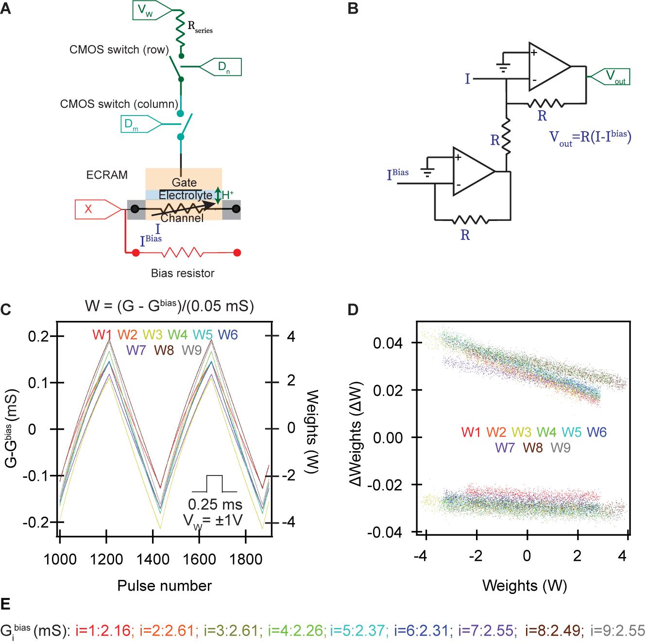
Figure 1. Organic ECRAM cells as electrochemical synapses. (A) Each synapse in the crossbar array contains one ECRAM, a discrete bias resistor used to obtain negative weights, a series resistor to control the gate current, and two CMOS switches as selectors. The ECRAM cells store synaptic weights by electrochemical doping/de-doping of the channel, which alters its electronic conductivity. When both switches are ON, the write current programs the redox transistor to the desired state. When either or both switches are OFF, the ECRAM cells retain their state. Two switches are used to accommodate the outer product update. (B) Subtractor circuit used to calculate the difference in the conductance between the ECRAM channel and the bias resistor; the same circuit is used when the currents from multiple devices are summed in an array. 10 kΩ resistors were used for Rseries in (A) and all resistors in (B). (C) Potentiation and depression of nine synapses, using pulses of identical magnitude. The resulting current (positive or negative) is used to calculate , where G_i is the electronic conductance of ECRAM i and is the conductance of the bias resistor, as written in (E). The non-dimensional weight is computed during post-processing by /(0.05mS). (D) Device-to-device variation of the nine synapses, showing the weight update for different starting weight values. Each device completed 50 full cycles, where each cycle equals 440 weight updates, equally divided amongst potentiation and depression. For clarity, a random 10% subset of the ∼20,000 weight updates for each device are shown. (E) The conductance values of the fixed discrete bias resistors.
Because large, rapid changes in the ion concentration in conducting polymers could result in rapid swelling and mechanical delamination, we utilize a series resistor to control the amount of current flowing into the ECRAM’s gate (Keene et al., 2018a; Fuller et al., 2019a). This series resistor is not needed in inorganic ECRAM cells because higher ionic resistance of the inorganic solid electrolyte is sufficient to limit the current (Fuller et al., 2017; Li et al., 2020a). The two CMOS switches are used to select the device to be programmed: weight updates are conducted only if both CMOS switches are ON; as we show later, one of these switches selects the rows and the other selects the columns that undergo weight updates, enabling parallel outer product updates of all devices in just one or two steps. This selection scheme differs from our past work utilizing a two-terminal diffusive memristor selector (Fuller et al., 2019a). While two CMOS switches will likely require larger chip area, it also results in more accurate and reliable switching by not using the more stochastic diffusive memristor. It also eliminates the extra “read-selector” CMOS switch previously used (Fuller et al., 2019a). In terms of functionality, the CMOS switches can be replaced with a single transistor switch, so the final synapse design is two transistor switches, one ECRAM, an offset bias resistor (or memristor) and one series resistor.
The sign of VW, common to all devices, controls the direction of the weight update, either potentiation (increase conductance) or depression (decrease conductance). A subtractor circuit is used to subtract the current between the channel and the bias resistor based on a proposed architecture in ref. (Agarwal et al., 2016; Figure 1B). The resulting current is measured using an operational transconductance amplifier, from which we can calculate by dividing this current from the input VR.
The linearity and reproducibility of the weight updates for the nine organic ECRAM cells are given in Figures 1C,D. The values are plotted in Figure 1C, where i indicates the index of the ECRAM cell. Using 0.25 ms write pulses, we obtain over 200 analog states for each device within the conductance range – the number of analog states in these devices can be changed by modifying the write time (Melianas et al., 2020). The equilibrium conductance G_i while the gate and channel are shorted is about 2.5 mS with some device-to-device variation. The conductance values of the bias resistors are listed within Figure 1. Although more desirable low-conductance devices in the nano-Siemens range were previously realized (Fuller et al., 2019a), this study used the higher conductance devices with greater fabrication reproducibility for proof-of-concept demonstration.
To obtain the non-dimensional synaptic weight W_i, we divide by 0.05 mS, and plot the values on the right axis of Figure 1C. In Figure 1D, we show the change in weight upon each applied write pulse, demonstrating low cycle-to-cycle and device-to-device variation across the nine ECRAM devices. An interesting feature is the higher slope, or nonlinearity, of ΔW vs. W upon potentiation over depression. One contributing factor is the ECRAM cells in the low-conductance state lose state faster due to oxidation with the ambient environment than cells in high-conductance states (Keene et al., 2018b; Melianas et al., 2020). Other electrochemical and electronic mechanisms also contribute to this nonlinearity and are subjects for future investigations.
We conduct parallel in-situ training of a simple perceptron network with two binary inputs (X1 and X2) and a bias input X3, which is always equal to 1. We use three outputs corresponding to the three logic gates that are trained in this experiment (Figure 2A); these represent three of the four linearly separable elementary logic gates containing two binary inputs, one bias input, and one output. For each logic gate, the training set consists of four examples corresponding to all possible values of X1 and X2; the training set is consecutively and iteratively used to train the ECRAM array until the network correctly identifies the entire training set for all logic gates. These logic gates were chosen due to the low number of devices available, which is a common challenge for emerging device technologies where fabrication processes have not been fully established.
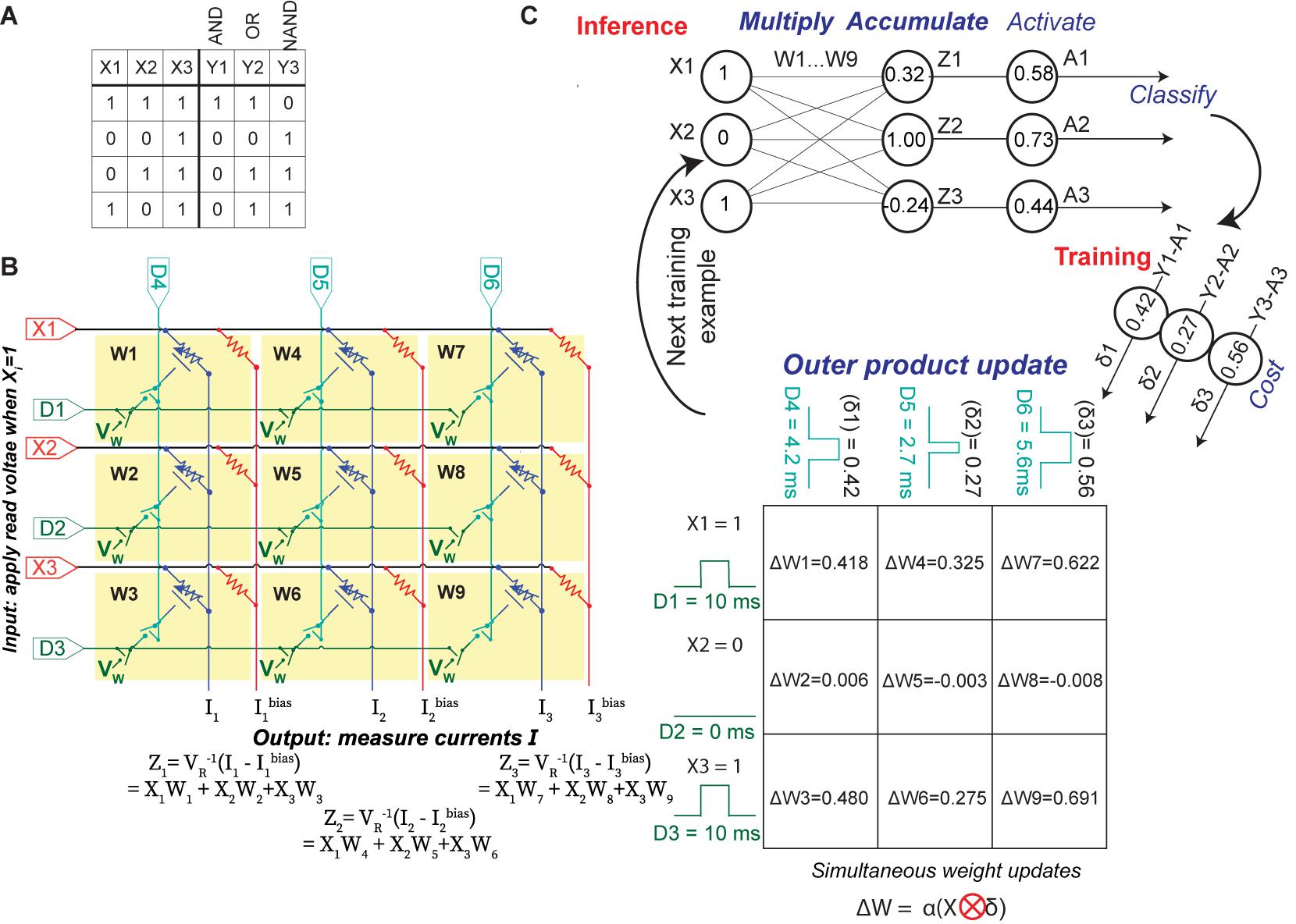
Figure 2. Implementation of parallel array learning. (A) List of the training examples in this work. The “X” represents the inputs fed into the three rows of the crossbar, while the outputs “Y” show the correct solutions and used to compute the cost functions of each column output. (B) Circuit schematic of the nine-ECRAM array. Each synapse W1–9 contains an element in Figure 1A; the series resistor is not shown here for legibility. During inference, the circuit measures I-Ibias using the subtractor circuit in Figure 1B, and this is converted to the non-dimensional software value Z. During weight updates, the digital inputs D1–6 are used to select the time that the switches are ON in each row and column, which controls the change in weight for each device in accordance with an outer product update. (C) Flow diagram of learning process. During inference, multiply and accumulate are conducted using the crossbar in the manner described in (B). Afterward, the activation energy and cost functions are computed in software and used to compute the weight update. To conduct a parallel outer product update, the pulse widths of digital switches D1–3 correspond to the inputs X1–3, while the pulse widths of digital switches D4–6 correspond to the cost δ1–3. Positive and negative weight changes must be conducted separately, so two steps are needed to conduct a parallel weight update.
Figures 2B,C shows the circuit and the flow diagram for both forward and backward propagation step based on stochastic gradient descent. The nine electrochemical synapses are electrically arranged into a 3 × 3 crossbar using a printed circuit board. To conduct forward propagation, or inference, the crossbar uses multiply-and-accumulate operations to perform the matrix operation Z = WTX, where W is the matrix of synaptic weights and X is the vector of input value. We apply a small read voltage (VR) ∼50 mV to represent a logical “high” at the input and measure the accumulated current at the bottom of each column, which is held at virtual ground using an operational amplifier. The vector-matrix product Z is proportional to the difference between the accumulated current of the ECRAM column and the accumulated current through the bias resistor column. It is computed by using a subtractor circuit (Figure 1B) in each column. Once this vector-matrix product is obtained, we compute the sigmoid activation function (A = σ (Z)) in software and compare the result to 0.5 to obtain the binary prediction. The error δ equals the solution Y minus the activation A: if the absolute value of δ for a column is less than 0.5, the network has correctly classified that column; if |δ| > 0.5, then the network has incorrectly classified the column.
Next, we describe how to train the network in parallel. The change in weight for the array is given by the outer product update where ⊗ denotes the outer product, is the derivative of the cost function ℒ=Ylog(A) + (1−Y)log(1−A) with respect to the vector-matrix product Z, and α is the learning rate. We choose cross-entropy as the cost function such that = Y-A = δ. In addition to the continuous-valued weight update, we also incorporated a discrete-value cross-entropy update scheme whereby we rounded δ to take the value of −1, 0, or 1 during weight updates. We demonstrate these two weight update schemes to show the broader generalizability of our approach.
To conduct the parallel outer product update, we simultaneously apply three sets of voltages to the circuit (Figure 2B). First, we apply a write voltage VW = 1V or −1V to all the synapses. Second, we apply a pulse to the “row” digital terminals D1–3 that equals 10 ms when Xi = 1 and 0 ms when Xi = 0; we note that these pulse widths can also be analog rather than binary. Third, we apply a variable-width pulse to the “column” digital terminals D4–6 that is proportional to α⋅δ for continuous-valued updates and α⋅round(δ) for discrete-value updates; α⋅δ=1 correspond to 10 ms. Since weight updates entail that both switches are ON, the weight of a synapse does not change when Xi = 0 during that training step. In other words, this pulse timing conducts an outer product multiplication between the input X on the “row” terminals and α⋅δ or α⋅round(δ) on the “column” terminals (Figure 2C).
This parallel weight update scheme is scalable to larger arrays: the outer product update enables all weights in an array to be updated by controlling the D terminals at the edges of the array, regardless of array sizes. Because the VW terminal is shared among all devices, two sequential sets of pulses are needed to update all weights, one to increase conductance weights (VW = −1V) and one to decrease weights (VW = 1V); we note that, if the inputs Xi can be negative, then four update cycles would be needed. The CMOS switches are used for selectivity and to prevent crosstalk: when the switches are OFF, the gates are electrically isolated from each other. The devices are also ionically isolated from each other during fabrication. In our training experiments, all values of W were collected for post-mortem processing and analysis, but this information was not used during training in order to demonstrate its parallelism.
The table in Figure 2C shows one example step of this parallel weight update using the continuous-valued cross-entropy cost function. This scheme enables accurate analog weight updates for all devices in parallel, where the changes in the device’s conductance nearly perfectly match the desired values; this will be quantified in detail later.
Experimental in situ Parallel Training
The four training examples, each using three logic operations (Figure 2A), are consecutively and iteratively fed into the network, until the network attains 100% accuracy as determined by when absolute errors |δ| decrease below 0.5 for all cases in the training set. Figure 3 shows the results of the training. After randomly seeding values for the initial condition, we show the evolution of synaptic weights in Figure 3A, where we utilize the continuous-value weight updates given by the cross-entropy cost function, after each training epoch. The updates to the weights decrease over time, signifying convergence. While the threshold for accuracy occurs when |δ| < 0.5, continued training epochs further decrease the error, which provide a margin against noise and other non-idealities.
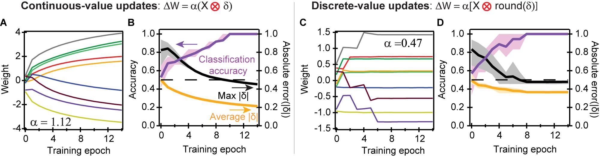
Figure 3. Convergence of perceptron operations using different learning rules. (A) Weight updates of the nine synapses using stochastic gradient descent to solve for AND, OR, and NAND logic gate functions. The cross-entropy cost function with continuous-value weight updates was used, such that = Y-A = δ. (B) Average accuracy and absolute error to train six different initial seed values; the shaded areas represent the range of values taken by the six seeds. It takes about ten training epochs to fully classify the problem. Our learning rule states that an absolute error |δ| less than 0.5 is a correct classification. The average absolute error takes the mean absolute error |δ| of the 12 operations defined in Figure 2A in each training epoch; the max error is the maximum error of the 12 classification operations. Convergence is defined as when the classification accuracy is 100%, or when the maximum error is less than 0.5. (C) Experimental training when using discrete-value weight updates: positive, negative, or 0. (D) Convergence, accuracy, and error for discrete-value updates, with the same colors defined in (B). The colors in (A,C) are the same as the ones defined in Figure 1C.
Figure 3B plots the fraction of twelve operations (four training examples multiplied by the three logic gates in Figure 2A) that were accurately classified, the average absolute value of the error (|δ|) across all twelve operations, and the maximum |δ| across the twelve operations. Figure 3B incorporates the results of six different random initial seeds: the dark lines equal the average values for all six seeds, while the lighter shaded areas equal the full range for the different seeds. When the maximum |δ| is less than 0.5, then all input cases representing the logical function have been correctly learned by the corresponding ECRAM devices. Our results show a gradual reduction in error, and an average of eight training epochs to reach the full classification accuracy.
Discrete-value weight updates result in somewhat different convergence behavior. Rather than slowly converging like the continuous case, the weights stop updating once all computed values of |δ| are below 0.5, and the problem is correctly classified (Figure 3C); changes in weight after this point reflect non-idealities, such as slight drift or rebound after weight weigh updates. This rebound may occasionally cause a temporary drop in classification accuracy when the weights are near the threshold of accuracy; this is quickly corrected during the next weight update.
While discrete-value weight updates achieve rapid convergence, the convergence rate is also more sensitive to the initial conditions. This results in a higher variability of the error and accuracy, as shown by the larger spread of the lighter shaded regions in Figure 3D. Because discrete-value weight updates have sharp ending thresholds, certain operations reside at the threshold of accuracy where δi∼0.5, providing less margin against possible drift, noise, and memory loss than the continuous-valued updates (Figure 3A).
One important difference is that the discrete-valued updates converge somewhat faster than continuous-valued updates. The reason is because discrete-value updates only update weights during incorrect classification, whereas continuous-value updates also update weights during correct classification, which may result in updates in the “wrong” direction.
As an example, suppose we solve for the OR gate when W4 = W5 = W6 = 0.4; a value of Z > 0 ultimately corresponds to logical 1 and Z < 0 to logical 0. This correctly classifies the first three training examples in Figure 2A but incorrectly classifies the fourth (X1 = X2 = 0). During discrete-value updates, only the incorrectly classified fourth training example will trigger weight updates. Full convergence is reached as soon as W6 < 0, which can happen in just a single training epoch. In contrast, during continuous-value updates, W4, W5, and W6 will increase during the first three training examples because 0 < |δ| < 0.5. These increases in W6 will counterbalance the decrease during the fourth training example, resulting in slower convergence. This process also increases the magnitude of W4 and W5, explaining why the weights are generally larger in the continuous-valued rather than discrete-valued updates. Another reason for the higher weight ranges of Figure 3A is because the weights continue to change even after convergence. Despite these differences, our training scheme can correctly classify the logic gates to full accuracy after several training epochs, for all six seed values initiated.
Crossbar Simulations Quantitatively Reproduce Experimental Data
Next, we conduct crossbar simulations using the same initial conditions to compare against experimental results. Two types of simulations are conducted. The “simulated” result accounts for nonlinearity, cycle-to-cycle variation, and device-to-device variation within the array by interpolating the switching data in Figures 1C,D to predict the results of each weight update for all nine devices. The “ideal numerical” result presents the values at the floating point precision of a simulated neural network.
Figure 4A shows the simulated weight evolution compared with the experiment using continuous-value weight updates based on the cross-entropy cost function. The agreement is near perfect, with a coefficient of determination R2 = 0.997. This agreement results from the low cycle-to-cycle variability and the highly deterministic and predictable switching behavior, such that the switching behavior during training is essentially identical to the switching behavior during ramping in Figures 1C,D. This enables quantitative agreement between the experimental and simulated conductance weight on each device. Figure 4B compares the experimental results to the ideal numerical weight evolution, which yields R2 = 0.937. Some deviations exist due to the slightly nonlinear switching behavior of the individual devices at high and low weights (Figures 1C,D) at the extremes of the potentiation and depression range; a recent formulation using p(gT2-TT) organic materials with a larger dynamic range could overcome this problem (Melianas et al., 2020). This nonlinearity is present in the experiment (Figure 3) and the simulation based on device data (Figure 4A), but not present in the “ideal” simulation at floating point precision (Figure 4B), making it more difficult to experimentally move the weights further away from 0.
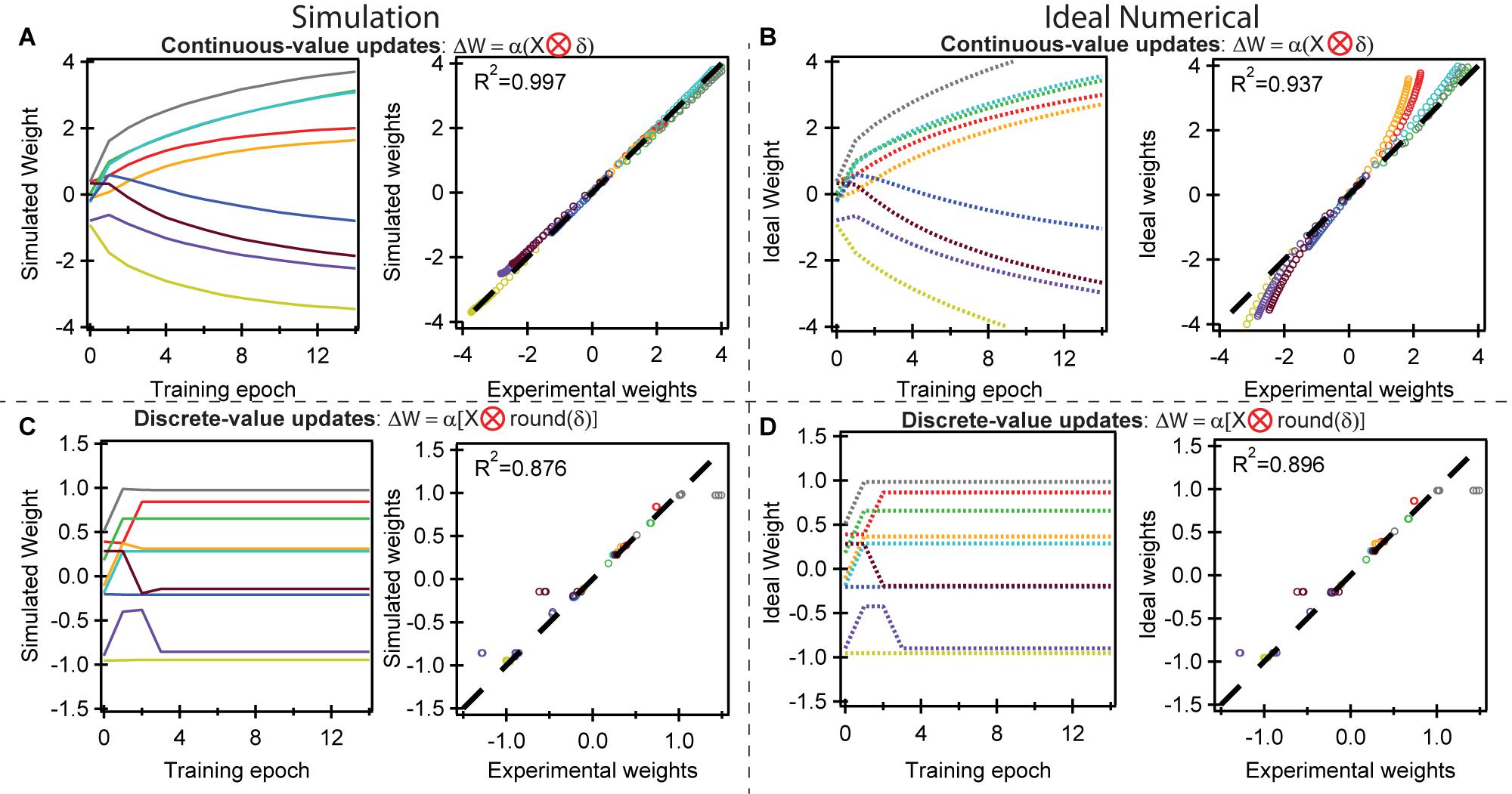
Figure 4. Simulated training behavior compared to the experimental behavior. (A) (left) Simulated weight evolution using the switching properties measured in Figures 1C,D. The results are essentially identical to the experimental results in Figure 3A. (right) A plot of the experimental vs. simulated weights show an R2 = 0.997, demonstrating that the simulations can fully replicate in-situ experimental training procedures. The weights across all epochs are plotted. (B) Ideal numerical weight evolution for the logic gates assuming perfectly linear and symmetric devices at floating point precision. There exist some deviations at higher and lower weights as a result of nonlinear and asymmetric switching behavior at the extremes of dynamic range in experimental ECRAM devices. (C,D) Comparison of simulated, ideal, and experimental results using the discrete-value rather than continuous-value weight updates. These show more deviations than (A,B) because slight variations in weights may result in an extra, relatively large weight update in the experimental results. All colors have the same meaning as in Figure 1C.
Figures 4C,D uses the discrete-value weight updates based on the same cross-entropy cost function. While the overall trend of the simulated weight evolution (Figure 4C) is similar to that of experiment (Figure 3C), some deviations are present such that R2 = 0.876. The origin of this deviation arises from slight deviations in the weights at the threshold of accuracy may result in an extra relatively large discrete weight update. In the ideal numerical case in Figure 4D, R2 = 0.896, about equal to that in Figure 4C. Unlike the case for the continuous-value updates, there is less effect of nonlinearity because the weight range is much narrower (+/−1.5 vs. +/−4.0), placing the devices in a conductance range where they operate more linear and ideal.
The results presented in Figures 3, 4 summarize the successful demonstration of in situ training using an ECRAM array: hardware parallel array training accompanied by a close match between device-level experiments and crossbar simulations.
Analysis of Experimental Training Accuracy
The excellent agreement between simulated and experimental training is a result of the excellent accuracy of the array to conduct the vector-matrix multiply and the outer product update. Figure 5A plots the accuracy of vector matrix multiply by comparing the Z obtained in analog manner directly by measuring the currents in each column of the crossbar and the Z obtained by measuring the weight of each device, then adding them in software using floating-point precision during post-processing. Our results show extremely high accuracy with an R2 value of 0.9996, suggesting that the network can conduct inference with essentially perfect accuracy.
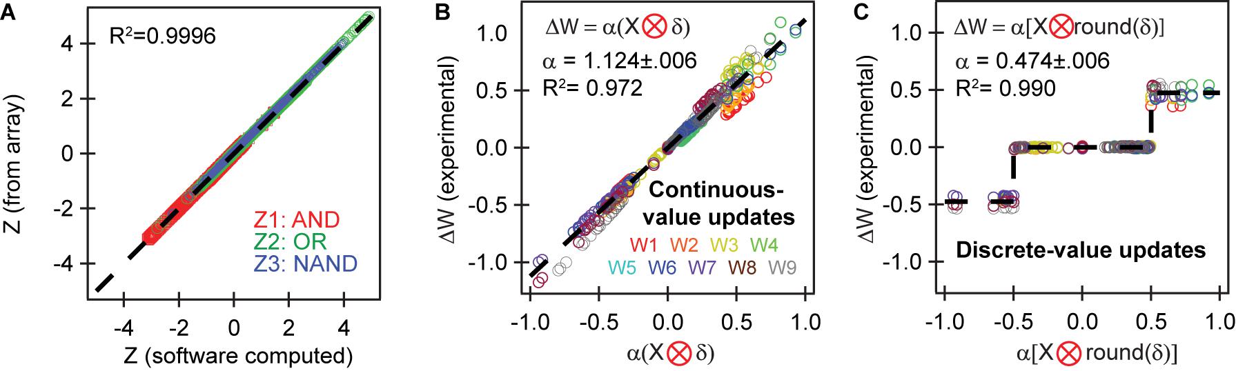
Figure 5. Accuracy of the analog matrix operations. The X axes computes the expected values for the vector matrix multiply and outer product update using software during post-processing. The Y axes plots the obtained value for Z and ΔW experimentally measured from the crossbar. (A) Vector-matrix multiply shows near-perfect agreement. (B,C) Outer product updates are conducted very accurately in accordance with defined cost functions and learning rules, with R2 over 97%, showing excellent goodness of fit. This result explains the strong convergence between the numerical and experimental results in Figure 4. The values for α were fit from the experimental vs. simulated outer product updates.
Figures 5B,C shows the accuracy of the parallel outer product updates for the continuous and discrete-value updates by plotting the expected ΔW computed from the error δ, against the actual weight change computed by measuring the synaptic weight before and after the weight update. R2 here ranges from 0.97 for continuous-value updates and 0.99 for discrete-value updates. This ensures that any desired weight update can be realized with very high accuracy. The high accuracy of outer product updates demonstrated here is a vast improvement over past works (Fuller et al., 2019a; Kim et al., 2019) in both individual device switching behavior as well as device-to-device variation, and is essential for reaching convergence. As we show in simulation later, this quality strongly facilitates achieving rapid convergence in more complex problems involving hidden layers.
Analysis of Nonlinearity and Variability
We quantitatively compare the performances of ECRAM devices with the metrics identified by Sun and Yu (2019). The key metrics for training are the degree of nonlinearity, which defines to what extent the weight (conductance) change ΔW changes with the weight W, the cycle-to-cycle variation, determined by the reproducibility of the switching processes within a device, and the device-to-device variation, which sets the variation in the nonlinearity between devices.
We applied the analytical methodology proposed by Sun and Yu (2019) to classify three additional classes of nonvolatile memory: the ECRAM cells used in this work, the SONOS floating-gate memory conducted in Agarwal et al. (2019), and the TaOx resistive random access memory (RRAM) cells from Bennett et al. (2019a). Table 1 summarizes these results.
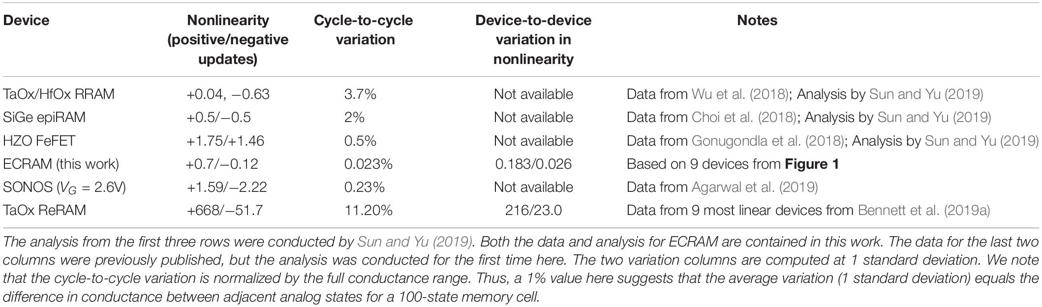
Table 1. Quantitative comparison of non-volatile devices for training based on the analysis protocol developed by Sun and Yu (2019).
According to Table 1, the nonlinearity of ECRAM is comparable to that of the best published TaOx/HfOx RRAM and SiGe epiRAM devices; the other devices show higher nonlinearity. ECRAMs excels in its low cycle-to-cycle variation because the electrochemical insertion and extraction of ions is much more deterministic and predictable than the stochastic formation of memristive filaments (Ielmini and Wong, 2018; Li et al., 2020a). As seen in Figure 1D, the ΔW values for ECRAM cells occur in a very narrow region.
Despite the excellent metrics of ECRAM with regards to nonlinearity and device-to-device variation, two additional factors need to be considered when interpreting these results. First, the ECRAM gate and channels are 750 μm × 2,000 μm each. Smaller devices, including ones scaled to sub-micron dimensions, were shown in past works (Tang et al., 2018; Melianas et al., 2020), but it has yet to be tested how downscaled devices perform relative to the metrics shown in Table 1. Second, ECRAM cells in this work have a high electronic conductance, which results in high read energies. Other organic (Fuller et al., 2019a) and inorganic (Tang et al., 2018; Li et al.,2020a,b) ECRAM cells with a channel conductance of ∼10 MΩ have been shown; however, the device-to-device variation between devices have not been studied in detail.
Array-Level Simulations of Training
Having validated the agreement between simulated and experimental results on a small array in Figure 4, we use simulation to systematically compare the classification accuracy of ECRAM and TaOx memristors at solving the three simple logic gates with a cross-entropy cost function and continuous-valued weight updates. Our numerical simulations are a significant advance over previous work by elucidating the effect of device-to-device variation, instead of only utilizing the properties of a single device. For the logic gates, we simulate a small 3 × 3 crossbar, identical to experiment, with 100 different initial conductance values as the “seed” conditions, and plot what percentage of the “seeds” yields full accuracy on all three logic gates. Because these logic gates are easier to classify than most machine learning problems, we use this more stringent definition of “percent full accuracy.”
Figure 6A shows the results of several simulations to show the effects of non-ideal behavior within a single device as well as the variation between devices. The first “ideal” simulation is the software implementation of the algorithm at floating point precision: in this simulation, all logic gates converge to 100% accuracy. The second simulation takes the switching behavior of a single ECRAM cell, which we denote as a lookup table (e.g., device W1 in Figure 1), and replicates that behavior for all devices. This “single ECRAM” accounts only for the effects of asymmetric nonlinearity and cycle to cycle variability, and the simulated crossbar essentially achieves the numerical limit at floating-point precision. Most past numerical simulations of crossbar accuracy in ECRAM generally present these two results.
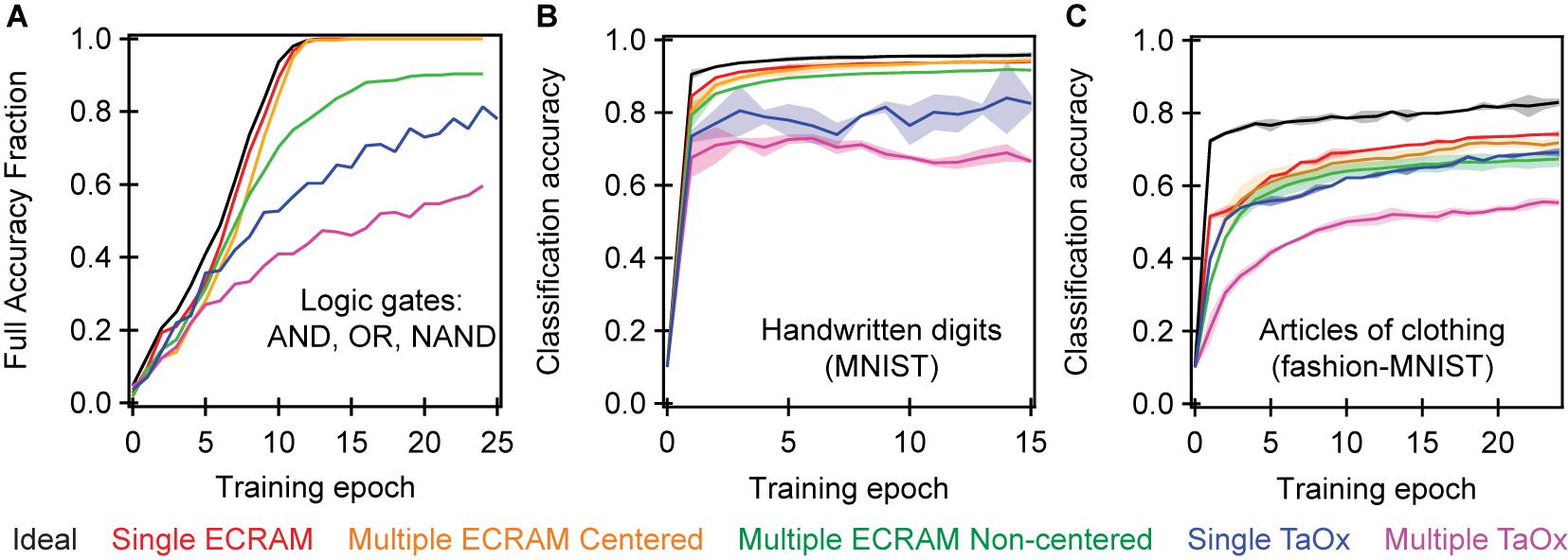
Figure 6. Simulated accuracy of (A) logic gates, (B) handwritten digits classification, and (C) articles of clothing classification. (A) used a single-layer 3 × 3 perceptron network like experiment; the full accuracy fraction denotes the fraction of seed values that are able to achieve 100% accuracy for all twelve permutations of for the three logic gates designed by Figure 2A. Two multi-layer perceptron networks, each with a single hidden layer, were simulated in (B) and (C). The accuracy denotes the fraction of the data that was correctly classified. The handwritten digits classification (B) used a 65 × 36 and a 37 × 10 crossbar, while the articles of clothing classification (C) used a 785 × 400 and a 401 × 10 crossbar. The single ECRAM and single TaOx memristor cases use the switching properties from a single device and assumes all devices are identical in the array. The multiple ECRAM and multiple TaOx cases account for device-to-device variation using interpolation between multiple device probabilistic maps (look-up-tables), as described in Agarwal et al. (2016) and Bennett et al. (2019a). Centered simulations correct for differences in the equilibrium conductance of the device, so they are all oriented around a single conductance value (as was done experimentally with bias devices) while the non-centered simulation does not perform this correction. All simulations show significant improvement of ECRAM over TaOx, as well as the importance of accounting for device-to-device variations. The shaded regions represent two standard deviations of the simulation, each conducted over 100 random “seed” initial weights.
The third simulation, denoted as “multiple ECRAM, centered,” accounts for some device-to-device variability by using all nine lookup tables. This simulation accounts for variation in switching behavior, such as certain devices being more sensitive or more nonlinear than others. However, this simulation also “centers” the range of all devices around a fixed value, as was done in Figure 1C. This can be realized in one of two ways: one approach is to reduce device-to-device variability by improved ECRAM fabrication process so that all ECRAM cells would have the same equilibrium conductance; a second method is to pair each ECRAM with a calibrated offset resistor, as was done in this work (Figures 1, 2B). We propose that the second method can be realized on-chip by using a paired non-volatile memory element like a memristor, that is initially programmed to approximately equal the equilibrium conductance of the ECRAM cell and not changed afterward. This memory element also serves to enable negative weights much like the bias resistor used in this work (Figure 1A). Our results show a slightly slower convergence in this case, but the accuracy nonetheless converges consistently. This simulation is similar to the conducted experiment (Figures 3A,B) and paired simulations (Figure 4A): the 8 epochs needed for half the simulated seeds to convergence is very similar to the ∼9 epochs needed on average for the six experimental seeds to converge in Figure 3B. All simulations in this section assume continuous-valued weight updates.
The fourth simulation, denoted as “multiple ECRAM, non-centered,” removes the “centering” process and accounts for the variable range of the different ECRAM cells. As shown by the values of the bias resistors in Figure 1, the devices’ equilibrium conductance ranges from 2.1 to 2.6 mS. This simulation shows that only ∼90% of the initial seeding conditions will converge to full accuracy. Unlike experiments and the third simulation, this fourth simulation does not fully converge because it chooses a common center-point for all devices; in other words, it is equivalent to using the same bias resistor, like 2.4 mS, for all synapses. Due to the different physical conductance ranges of various devices, the switching properties for some devices around the global centerpoint are different from that of the other devices around the same value. This results in non-uniform and nonlinear weight update behavior. The reduction in accuracy here shows the crucial importance of having devices with the same center conductance, or finding a method to correct for this such as by using bias resistors.
We also conduct two simulations using TaOx memristors based on the switching properties published previously (Bennett et al., 2019a). As shown in Table 1, this dataset contains both nonlinearity and device-to-device variation data. This result shows that ∼ 80% of the initial conditions fully converge when replicating the properties of a single device (“single TaOx”) and ∼50% fully converge when accounting for device-to-device variation (“many TaOx”). This simulation shows that ECRAM has significant advantages in terms of training accuracy even in the case of simple logic gate functions. It further shows that attaining full accuracy for the 100 simulated seeds in logic gates, as done experimentally with ECRAM, is a nontrivial task that requires excellent individual device switching properties.
We simulate the accuracy of the same devices for image classification of handwritten digits, using a downsampled version of the MNIST database known as the UCI Optical Character Recognition (OCR) task (Alpaydin and Kaynak, 1998), and articles of clothing, from the more recently developed Fashion-MNIST database (Xiao et al., 2017) in Figures 6B,C. Each task contains ten categories or classes. Because these images are harder to classify than the logic gate inputs, we plot the average fraction of correctly identified solutions for the 100 simulated seeds, as opposed to the fraction of simulated seeds that achieve 100% accuracy. The chosen two-layer network topology consists of a 65 × 36 crossbar followed by a 37 × 10 crossbar – the outputs from the first crossbar, plus a bias input, are used as inputs for the second crossbar. A 95% accuracy is achieved on the handwritten digits task in the numeric limit. All ECRAM simulations yield above 91% accuracy, while the TaOx simulations yield significantly lower accuracies. The fashion-MNIST network yields just 83% accuracy at the numerical limit, due to the greater complexity and nonlinearity of the classification problem, with progressively lower accuracies for ECRAM and TaOx. This simulation also utilized a two layer network, but this time consisting of a 785 × 400 and a 401 × 10 crossbar. Once again, the outputs form the first crossbar plus a bias input are used as inputs for the second crossbar.
All simulations show that ECRAM outperforms TaOx under any configuration. However, TaOx simulations appear more inaccurate in handwritten digits than in articles of clothing because the handwritten digits require higher learning rates, such that the nonlinear behavior of the filamentary memristors more significantly decrease the accuracy (see methods for exact numbers). In contrast, articles of clothing utilize lower learning rates, and a lower theoretical accuracy using fully connected networks. The lower learning rates are more resilient to device nonlinearity, such that the single-device TaOx accuracy nears that of ECRAM. This work further work shows the importance of multiple metrics in characterizing the accuracy of different devices.
Our results further show that device-to-device variation plays a significant role in the accuracy of in-situ training networks. In memristors, device-to-device variation is an intrinsic property relating to the discrete, stochastic nature of atomic point defects within the conductive filament (Yu et al., 2013; Ielmini and Wong, 2018). For ECRAM, our observed device-to-device variation likely result from an unoptimized fabrication process. Specifically, the ECRAMs in this work were fabricated using solution-processing followed by lift-off (Khodagholy et al., 2011), which enables rapid prototyping but is not well suited for reduced device-to-device variability. This device-to-device variability will likely be more significant for devices with lower conductances, such as the nano-Siemen devices shown in past work (Fuller et al., 2019a), which would likely result in lower weight tuning and training accuracy. The lift-off method can be replaced by more advanced lithography techniques to improve device yield and areal density.
Our simulations again highlight two different types of device-to-device variation within ECRAM, one primarily behavioral and relating to differences in slightly distinct switching properties among each device’s probabilistic switching map (from “single ECRAM” to “many ECRAM, centered”), and the other relating to range-derived differences in the equilibrium conductance (from “many ECRAM, centered” to “many ECRAM, non-centered”). While both should improve with better fabrication and processing, we anticipate the latter equilibrium conductance is simpler to tackle because the conductance is determined by PEDOT:PSS film uniformity across the wafer die. In contrast, the switching variability depends on the uniformity in the entire multilayer PEDOT:PSS/electrolyte stack and the associated charge transfer kinetics within this stack, which may be more difficult to control. If ECRAM provides the elusive memory element for parallel in situ learning, our approach paves the way toward massively parallel training of artificial neural networks at unprecedented levels of energy efficiency.
ECRAM for Deep and Spiking Neuronal Learning Methods
We further consider how the in situ learning approaches we present in this work could be extended to spiking neural networks (SNNs). Unlike multilayer perceptron networks (e.g., deep neural networks and convolutional neural networks) that transmit information at each propagation cycle, neurons in SNNs are only activated when their activation reaches the threshold potential. By encoding information more sparsely in the temporal domain and restricting the analog requirements for information transmission, SNNs are widely considered more likely to achieve the energy efficiency and error tolerance of biological computing system (Wang et al., 2020). Spike time-dependent plasticity (STDP) like functionality have been demonstrated in organic and inorganic ECRAM (van de Burgt et al., 2017; Sharbati et al., 2018; Li et al., 2020b). While STDP or STPD-like rules do not directly implement stochastic gradient descent backpropagation, they effectively sample an input and may approximate a statistical method known as expectation maximization (Nessler et al., 2013).
Numerical approaches to derive loss functions based on spike learning have been proposed (Shrestha et al., 2019), although it is not clear how well these approaches scale with multiple spiking hidden layers. However, the complexity of implementing these rules is typically simpler in nanosynapses, since STDP does not require synaptic linearity, and may even be able to exploit some degree of synaptic non-linearity (Querlioz et al., 2013). Yet STDP-style learning systems still require minimum synaptic analog resolution, as well as symmetry between programming/update modes. Shallow or sampling networks can effectively implement STDP learning with 4–5 bit resolution (Pfeil et al., 2012; Woods et al., 2015). In addition, the requirements may be relaxed even further when using a technique known as the Linear Solutions of Higher Dimensional Interlayers to improve the linear separability of a machine learning (Tapson et al., 2013), which was recently demonstrated for emerging device crossbar based systems (Bennett et al., 2019b).
Although the stringency requirements for implementing SNN learning may be lower than for stochastic gradient descent, this study’s focus on reliable analog switching, including realistic considerations of device-to-device and cycle-to-cycle variation, will be an asset to future works on this topic. For instance, our analysis that synaptic conductance range centering is critical to implementing effective parallel updates may be equally advantageous to realizing SNN layer-by-layer learning that is parallelizable. A lower bound estimate of cycle-to-cycle noise tolerable on STDP learning has not been established in the literature, but may be better interrogated given our approach. Conversely, from the perspective of device optimization for efficient SNN implementation, the analog depth, low cycle-to-cycle noise, and good mode symmetry of ECRAM devices suggest these devices will be strong candidates for hardware SNNs. In contrast, while phase-change memory has recently been used to physically realize STDP learning they have substantial asymmetry between SET and RESET modes (Ambrogio et al., 2016). This creates additional circuit overhead for accessing synapses on dense crossbars and damps the maximal efficiency possible with local learning rules. STDP, short term potentiation, and paired pulse facilitation has already been demonstrated in organic ECRAM devices similar to those presented here (van de Burgt et al., 2017). Importantly, ion transport kinetics and material composition play decisive roles in determining the temporal response and, therefore, are likely to similarly affect efficiency and accuracy of the spiking timing based learning algorithms. Our work therefore strongly encourages further investigation of three-terminal ECRAM devices for modern SNN learning.
Conclusion
In summary, we experimentally achieve parallel in situ training using organic ECRAM synapses with high accuracy, a necessary step toward realizing efficient and accurate hardware training accelerators. Moreover, we show unprecedented reproducibility between the simulated and experimental training results, not just in the number of epochs to convergence but the exact evolution of the weight of each synapse. By experimentally demonstrating training using outer product updates that are consistent with numerical simulations, our work implies the potential of ECRAM cells to ultimately contribute to high accuracy in neural network training accelerators, and affirms the ability of our software methodology to contribute to leading toward this important goal.
Materials and Methods
Fabrication of ECRAM Cells
The ECRAM devices were patterned as reported previously (Fuller et al., 2019a; Melianas et al., 2020). Briefly, Ti(8 nm)/Au(50 nm) electrodes were patterned on Si wafers with 1 μm thick SiO2 using e-beam evaporation. The wafers were then coated with 1.5 μm parylene C as the insulating layer which was crosslinked with the adhesion promoter 3-(trimethoxysilyl)propyl methacrylate. After coating the first parylene C layer, a dilute soap solution (3% Micro-90 in H2O) was spincoated on top, followed by coating another 1.5 μm layer of parylene C. The wafers were then coated with 75 nm Ti and were subsequently patterned and dry-etched to define the channel, gate, and electrode pad areas. In this work, each wafer die had 8 devices. Before PEDOT:PSS deposition, the wafer dies were cleaned using 5 min sonication in isopropanol followed by 5 min UV-Ozone treatment. PEDOT:PSS was spincoated on the wafer dies in ambient at 1000 rpm for 2 min and baked at 120°C for 20 min. The top parylene C layer was then peeled off, leaving PEDOT:PSS only in the photolithographically defined channel, gate, and contact pad regions. Before electrolyte deposition, the wafer die was rinsed in H2O to remove residual Micro-90. The ion gel electrolyte (Melianas et al., 2020) was then drop-cast on top of each device using a micropipette.
Finally, the chips were wire-bonded onto a PLCC-68 chip carrier and breakout board to address the many circuit leads of the board.
Circuit Design
The circuit was implemented on a four-layer printed circuit board (PCB) fabricated by Gorilla Circuits (San Jose, CA, United States). Molex connectors were used to connect the PCB to the wire-bonded ECRAM chips. All other active (e.g., CMOS switches, op-amps) and passive (e.g., discrete resistors, capacitors) circuit components are also placed and wired using the printed circuit board. In addition to the circuit and components shown in Figure 2B, the PCB also includes a current subtraction circuit (Figure 1B) and an operational transconductance amplifier for each output column in order to convert the multiply-and-accumulate output current into a voltage that can be logged by a data acquisition instrument (NI-DAQ).
The three analog inputs X1–3 were connected to three analog outputs from a NI-DAQ, PCIe-6363; the read voltage is typically ∼50 mV. The write voltage (VW = +/−1V), common to all cells, were also connected to a fourth analog output from the NI-DAQ. The output voltage from the operational transconductance amplifier were connected to the analog inputs of a NI-DAQ. The NI-DAQ was controlled using a custom-built LabVIEW software.
Crossbar Array Control
A custom-built Python package served as the user interface with the LabVIEW software used to control the DAQ. Each time step is 0.1 s. To conduct inference, a 50-mV read voltage was applied to each row i where Xi = 1, and 0-mV applied when Xi = 0 for 10 ms. The currents read at the bottom represents the results of the multiply-and-accumulate function. Digital outputs D1–6 were held at low (0V) to keep the switches OFF and prevent leakage current. To conduct array training, the voltage VW was held at either +1 for depression or −1 for potentiation. The outer production selection is conducted through the pulse widths of the digital switches. D1–3 has a pulse width of 10 ms when X1–3 = 1, and 0 ms when X1–3 = 0. The pulse width of D4–6 is proportional to α⋅δ for continuous-value updates and α⋅round(δ) for discrete-value updates. A training epoch is defined as iterating this process through all four training examples.
Finally, to measure the conductance of individual array elements, 10-ms read voltage pulses were separately applied to each row of the crossbar. Because this voltage is applied to only one of X1, X2, or X3 at a time, the read currents at the bottom equals , where I_i is the current through ECRAM cell i while is the current through the paired bias resistor. We note that this step is a diagnostic measure, and the results were only recorded for post-processing and data analysis, and not using during in situ training.
Crossbar Simulations
Crossbar simulations were conducted on an expanded version of the open-source Sandia CrossSim simulation package, which is written in Python and allows for physics-realistic simulation of neural network accelerators. For the in situ learning case, which is the focus of this work, CrossSim instantiates neural cores with a variety of parameter corresponding to both device properties (conductance evolution behavior) as well as general neural network properties, such as network topology, choice of task, and learning rates. In order to effectively match the simulations with experiment, a custom set of look-up-tables (LUT) have been constructed by using experimentally derived sets of repeated ramped pulses. The LUT for ECRAM are given in Figure 1D, while the LUT for TaOx were taken from past work (Bennett et al., 2019a). This probabilistic matrix of look-up-tables is represented here as ΔGi(Gi), signifying that the change in conductance is a function of the present conductance. Then, when conducting backpropagation, globally requested updates applied to the logical cores via an outer-product-update (OPU) are individualized to simulated devices in the crossbar. The change in simulated weight is proportional to the product of ΔGi(Gi) and the results of the OPU [X⊗δ or X⊗round(δ)].
The simulations in Figures 4A,C were conducted by initializing, or seeding, the simulations at the same weights as the experiment, and using the LUT for each device. The ideal numerical simulations in Figures 4B,D were conducted assuming perfectly linear and symmetric devices: all ΔGi are identical for all device and all G.
The simulations in Figure 6 used 100 random initial seed values. Figure 6A plot the fraction of seed values that will achieve 100% classification accuracy of the twelve permutations of the logic gates trained in experiment (Figure 2A). Figures 6B,C plots average classification accuracy of the data set across all seeds. The learning rate for handwritten digits were 0.01 for numeric, 0.006 for single lookup table, and 0.012 for multiple lookup tables. The learning rate for articles of clothing were 0.001 for numeric, 0.0001 for single lookup table, and 0.00015 for multiple lookup tables.
The “ideal numerical” simulations in Figure 6 assumes that ΔGi is equal for all devices and conductance states. The single-ECRAM and single-TaOx uses the same LUT from one device to simulate all device properties in the array. The multiple-ECRAM for logic gates uses the same nine LUT from the experiment (Figure 1D). The other multiple-ECRAM and all multiple TaOx simulations picked random LUT from the dataset, with each simulated synapse drawing a random LUT. More details on CrossSim’s methodology and details of parameterized neural core operations can be found at: https://cross-sim.sandia.gov/_assets/documents/crosssim_manual.pdf.
Data Availability Statement
The datasets presented in this study can be found in online repositories. The names of the repository/repositories and accession number(s) can be found below: Materials Commons 2.0: https://doi.org/10.13011/m3-13da-my32.
Author Contributions
YL, EF, and AT conceived the project. AM fabricated the ECRAM devices. HT, EI, and YL designed the printed circuit board. EI, YL, and EF wrote the firmware and software for the measurements. YL conducted the measurements and analyzed the results. TX and CB conducted the simulations. All authors contributed to the writing of the manuscript.
Funding
This work was supported by the Sandia National Laboratories, the Laboratory Directed Research and Development (LDRD) Programs, including the Harry Truman Fellowship Program (YL). Sandia National Laboratories was a multimission laboratory managed and operated by the National Technology and Engineering Solutions of Sandia, LLC (NTESS), a wholly owned subsidiary of Honeywell International Inc., for the U. S. Department of Energy’s National Nuclear Security Administration under contract DE-NA-0003525. AM acknowledges support from the Knut and Alice Wallenberg Foundation (KAW 2016.0494) for Postdoctoral Research at Stanford University. AS acknowledges financial support from the National Science Foundation and the Semiconductor Research Corporation, E2CDA award ECCS-1739795. Part of this work was performed at the nano@Stanford labs, which were supported by the National Science Foundation as part of the National Nanotechnology Coordinated Infrastructure under award ECCS-1542152.
Conflict of Interest
YL, TX, CB, EI, HT, MM, EF, and AT were employed at Sandia National Laboratories by NTESS. The authors declare that this study received funding from the sources listed in the “funding sources” section. Sandia National Laboratories/NTESS verified that this study contains no classified information in order to approve its submission for publication. Otherwise, the funders were not involved in the study design, collection, analysis, interpretation of data, the writing of this article, or the decision to submit it for publication.
The handling editor declared a past co-authorship with several of the authors AM, AT, AS, and EF.
Acknowledgments
This manuscript describes objective technical results and analysis. Any subjective views or opinions that might be expressed in the manuscript do not necessarily represent the views of the U.S. Department of Energy or the United States Government.
References
Agarwal, S., Garland, D., Niroula, J., Jacobs-Gedrim, R. B., Hsia, A., Van Heukelom, M. S., et al. (2019). Using floating-gate memory to train ideal accuracy neural networks. IEEE J. Explor. Solid State Comput. Devices Circuits 5, 52–57. doi: 10.1109/JXCDC.2019.2902409
Agarwal, S., Plimpton, S. J., Hughart, D. R., Hsia, A. H., Richter, I., Cox, J. A., et al. (2016). “Resistive memory device requirements for a neural algorithm accelerator,” in Proceedings of the 2016 International Joint Conference on Neural Networks (IJCNN), Vancouver, BC, 929–938. doi: 10.1109/IJCNN.2016.7727298
Alibart, F., Zamanidoost, E., and Strukov, D. B. (2013). Pattern classification by memristive crossbar circuits using ex situ and in situ training. Nat. Commun. 4:2072. doi: 10.1038/ncomms3072
Alpaydin, E., and Kaynak, C. (1998). Optical Recognition of Handwritten Digits Data Set. UCI Machine Learning Repository. Oakland, CA: University of California.
Ambrogio, S., Ciocchini, N., Laudato, M., Milo, V., Pirovano, A., Fantini, P., et al. (2016). Unsupervised learning by spike timing dependent plasticity in phase change memory (PCM) synapses. Front. Neurosci. 10:56. doi: 10.3389/fnins.2016.00056
Ambrogio, S., Narayanan, P., Tsai, H., Shelby, R. M., Boybat, I., Di Nolfo, C., et al. (2018). Equivalent-accuracy accelerated neural-network training using analogue memory. Nature 558, 60–67. doi: 10.1038/s41586-018-0180-5
Bayat, F. M., Prezioso, M., Chakrabarti, B., Nili, H., Kataeva, I., and Strukov, D. (2018). Implementation of multilayer perceptron network with highly uniform passive memristive crossbar circuits. Nat. Commun. 9:2331. doi: 10.1038/s41467-018-04482-4
Bennett, C. H., Garland, D., Jacobs-Gedrim, R. B., Agarwal, S., and Marinella, M. J. (2019a). “Wafer-Scale TaOx device variability and implications for neuromorphic computing applications,” in Proceedings of the 2019 IEEE International Reliability Physics Symposium, (Piscataway, NJ: IEEE). doi: 10.1109/IRPS.2019.8720596
Bennett, C. H., Parmar, V., Calvet, L. E., Klein, J. O., Suri, M., Marinella, M. J., et al. (2019b). Contrasting advantages of learning with random weights and backpropagation in non-volatile memory neural networks. IEEE Access 7, 73938–73953. doi: 10.1109/ACCESS.2019.2920076
Burr, G. W., Shelby, R. M., Sebastian, A., Kim, S., Kim, S., Sidler, S., et al. (2017). Neuromorphic computing using non-volatile memory. Adv. Phys. X 2, 89–124. doi: 10.1080/23746149.2016.1259585
Cai, F., Correll, J. M., Lee, S. H., Lim, Y., Bothra, V., Zhang, Z., et al. (2019). A fully integrated reprogrammable memristor– CMOS system for efficient multiply–accumulate operations. Nat. Electron. 2, 290–299. doi: 10.1038/s41928-019-0270-x
Choi, S., Tan, S. H., Li, Z., Kim, Y., Choi, C., Chen, P. Y., et al. (2018). SiGe epitaxial memory for neuromorphic computing with reproducible high performance based on engineered dislocations. Nat. Mater. 17, 335–340. doi: 10.1038/s41563-017-0001-5
Emelyanov, A. V., Lapkin, D. A., Demin, V. A., Erokhin, V. V., Battistoni, S., Baldi, G., et al. (2016). First steps towards the realization of a double layer perceptron based on organic memristive devices. AIP Adv. 6:111301. doi: 10.1063/1.4966257
Fuller, E. J., El Gabaly, F., Léonard, F., Agarwal, S., Plimpton, S. J., Jacobs-Gedrim, R. B., et al. (2017). Li-Ion synaptic transistor for low power analog computing. Adv. Mater. 29:1604310. doi: 10.1002/adma.201604310
Fuller, E. J., Keene, S. T., Melianas, A., Wang, Z., Agarwal, S., Li, Y., et al. (2019a). Parallel programming of an ionic floating-gate memory array for scalable neuromorphic computing. Science 364, 570–574. doi: 10.1126/science.aaw5581
Fuller, E. J., Li, Y., Bennet, C., Keene, S. T., Melianas, A., Agrawal, S., et al. (2019b). Redox transistors for neuromorphic computing. IBM J. Res. Dev. 63:9:1–9:9. doi: 10.1147/JRD.2019.2942285
Gokmen, T., and Vlasov, Y. (2016). Acceleration of deep neural network training with resistive cross-point devices: design considerations. Front. Neurosci. 10:333. doi: 10.3389/fnins.2016.00333
Gonugondla, S. K., Kang, M., and Shanbhag, N. (2018). “A 42pJ/decision 3.12TOPS/W robust in-memory machine learning classifier with on-chip training,” in Proceedings of the 2018 IEEE International Solid-State Circuits Conference, San Francisco, CA, 490–492. doi: 10.1109/ISSCC.2018.8310398
Guo, X., Bayat, F. M., Bavandpour, M., Klachko, M., Mahmoodi, M. R., Prezioso, M., et al. (2017). “Fast, energy-efficient, robust, and reproducible mixed-signal neuromorphic classifier based on embedded NOR flash memory technology,” in Proceedings of the 2017 International Electron Devices Meeting, San Francisco, CA. 17:151–17:154. doi: 10.1109/IEDM.2017.8268341
Hu, M., Graves, C. E., Li, C., Li, Y., Ge, N., Montgomery, E., et al. (2018). Memristor-Based analog computation and neural network classification with a dot product engine. Adv. Mater. 30:1705914. doi: 10.1002/adma.201705914
Ielmini, D., and Wong, H. S. P. (2018). In-memory computing with resistive switching devices. Nat. Electron. 1, 333–343. doi: 10.1038/s41928-018-0092-2
Jacobs-Gedrim, R. B., Agarwal, S., Knisely, K. E., Stevens, J. E., van Heukelom, M. S., Hughart, D. R., et al. (2017). “Impact of linearity and write noise of analog resistive memory devices in a neural algorithm accelerator,” in Proceedings of the 2017 IEEE International Conference on Rebooting Computing, (Piscataway, NJ: IEEE), 17413472. doi: 10.1109/ICRC.2017.8123657
Keene, S. T., Melianas, A., Fuller, E. J., Van De Burgt, Y., Talin, A. A., Salleo, A., et al. (2018a). Optimized pulsed write schemes improve linearity and write speed for low-power organic neuromorphic devices. J. Phys. D Appl. Phys. 51:224002.
Keene, S. T., Melianas, A., Van de Burgt, Y., and Salleo, A. (2018b). Mechanisms for enhanced state retention and stability in redox-gated organic neuromorphic devices. Adv. Electron. Mater. 5:1800686. doi: 10.1002/aelm.201800686
Khodagholy, D., Gurfinkel, M., Stavrinidou, E., Leleux, P., Herve, T., Sanaur, S., et al. (2011). High speed and high density organic electrochemical transistor arrays. Appl. Phys. Lett. 99, 99–102. doi: 10.1063/1.3652912
Kim, S., Todorov, T., Onen, M., Gokmen, T., Bishop, D., Solomon, P., et al. (2019). “Metal-oxide based, CMOS-compatible ECRAM for deep learning accelerator,” in Proceedings of the 2019 International Electron Devices Meeting, San Francisco, CA, 847–850. doi: 10.1109/IEDM19573.2019.8993463
Lecun, Y., Bengio, Y., and Hinton, G. (2015). Deep learning. Nature 521, 436–444. doi: 10.1038/nature14539
Lee, S.-T., and Lee, J.-H. (2020). Neuromorphic computing using NAND flash memory architecture with pulse width modulation scheme. Front. Neurosci. 14:571292. doi: 10.3389/fnins.2020.571292
Li, C., Belkin, D., Li, Y., Yan, P., Hu, M., Ge, N., et al. (2018a). Efficient and self-adaptive in-situ learning in multilayer memristor neural networks. Nat. Commun. 9:2385. doi: 10.1038/s41467-018-04484-2
Li, C., Hu, M., Li, Y., Jiang, H., Ge, N., Montgomery, E., et al. (2018b). Analogue signal and image processing with large memristor crossbars. Nat. Electron. 1, 52–59.
Li, Y., Fuller, E. J., Asapu, S., Agarwal, S., Kurita, T., Yang, J. J., et al. (2019). Low-Voltage, CMOS-Free synaptic memory based on LiXTiO2 redox transistors. ACS Appl. Mater. Interfaces 11, 38982–38992. doi: 10.1021/acsami.9b14338
Li, Y., Fuller, E. J., Yoo, S., Ashby, D. S., Bennett, C. H., Horton, R. D., et al. (2020a). Filament-free bulk resistive memory enables deterministic analogue switching. Adv. Mater. 32:2003984. doi: 10.1002/adma.202003984
Li, Y., Lu, J., Shang, D., Liu, Q., Wu, S., Wu, Z., et al. (2020b). Oxide−Based electrolyte−gated transistors for spatiotemporal information processing. Adv. Mater. 32:2003018. doi: 10.1002/adma.202003018
Lin, Y. P., Bennett, C. H., Cabaret, T., Vodenicarevic, D., Chabi, D., Querlioz, D., et al. (2016). Physical realization of a supervised learning system built with organic memristive synapses. Sci. Rep. 6:31932. doi: 10.1038/srep31932
Marinella, M. J., Member, S., Agarwal, S., Hsia, A., Jacobs-gedrim, R., Niroula, J., et al. (2017). Multiscale co-design analysis of energy, latency, area, and accuracy of a ReRAM analog neural training accelerator. IEEE J. Emerg. Sel. Top. Circuits Syst. 8, 86–101. doi: 10.1109/JETCAS.2018.2796379
Melianas, A., Quill, T. J., LeCroy, G., Tuchman, Y., Loo, H. v., Keene, S. T., et al. (2020). Temperature-resilient solid-state organic artificial synapses for neuromorphic computing. Sci. Adv. 6:eabb2958. doi: 10.1126/sciadv.abb2958
Nandakumar, S. R., Le Gallo, M., Piveteau, C., Joshi, V., Mariani, G., Boybat, I., et al. (2020). Mixed-Precision deep learning based on computational memory. Front. Neurosci. 14:406. doi: 10.3389/fnins.2020.00406
Nawrocki, R. A., Voyles, R. M., and Shaheen, S. E. (2016). A mini review of neuromorphic architectures and implementations. IEEE Trans. Electron Devices 63, 3819–3829. doi: 10.1109/TED.2016.2598413
Nessler, B., Pfeiffer, M., Buesing, L., and Maass, W. (2013). Bayesian computation emerges in generic cortical microcircuits through spike-timing-dependent plasticity. PLoS Comput. Biol. 9:1003037. doi: 10.1371/journal.pcbi.1003037
Park, Y., and Lee, J. S. (2017). Artificial synapses with short- and long-term memory for spiking neural networks based on renewable materials. ACS Nano 11, 8962–8969. doi: 10.1021/acsnano.7b03347
Pfeil, T., Potjans, T. C., Schrader, S., Potjans, W., Schemmel, J., Diesmann, M., et al. (2012). Is a 4-Bit synaptic weight resolution enough? – constraints on enabling spike-timing dependent plasticity in neuromorphic hardware. Front. Neurosci. 6:90. doi: 10.3389/fnins.2012.00090
Prezioso, M., Hoskins, B. D., Adam, G. C., Likharev, K. K., and Strukov, D. B. (2015). Training and operation of an integrated neuromorphic network based on metal-oxide memristors. Nature 521, 61–64. doi: 10.1038/nature14441
Querlioz, D., Bichler, O., Dollfus, P., and Gamrat, C. (2013). Immunity to device variations in a spiking neural network with memristive nanodevices. IEEE Trans. Nanotechnol. 12, 288–295. doi: 10.1109/TNANO.2013.2250995
Sebastian, A., Le Gallo, M., Khaddam-Aljameh, R., and Eleftheriou, E. (2020). Memory devices and applications for in-memory computing. Nat. Nanotechnol. 15, 529–544. doi: 10.1038/s41565-020-0655-z
Sharbati, M. T., Du, Y., Torres, J., Ardolino, N. D., Yun, M., and Xiong, F. (2018). Low-Power, electrochemically tunable graphene synapses for neuromorphic computing. Adv. Mater. 30:1802353. doi: 10.1002/adma.201802353
Shrestha, A., Fang, H., Wu, Q., and Qiu, Q. (2019). “Approximating back-propagation for a biologically plausible local learning rule in spiking neural networks,” in Proceedings of the ICONS ‘19th International Confernece on Neuromorphic Systems, (New York, NY: ACM), 10. doi: 10.1145/3354265.3354275
Sun, X., and Yu, S. (2019). Impact of non-ideal characteristics of resistive synaptic devices on implementing convolutional neural networks. IEEE J. Emerg. Sel. Top. Circuits Syst. 9, 570–579. doi: 10.1109/JETCAS.2019.2933148
Sze, V., Chen, Y. H., Yang, T. J., and Emer, J. S. (2017). Efficient processing of deep neural networks: a tutorial and survey. Proc. IEEE 105, 2295–2329. doi: 10.1109/JPROC.2017.2761740
Tang, J., Bishop, D., Kim, S., Copel, M., Gokmen, T., Todorov, T., et al. (2018). “ECRAM as scalable synaptic cell for high-speed, low-power neuromorphic computing,” in Proceedings of the 2018 International Electron Devices Meeting, San Francisco, CA, 18:292–18:295. doi: 10.1109/IEDM.2018.8614551
Tapson, J. C., Cohen, G. K., Afshar, S., Stiefel, K. M., Buskila, Y., Wang, R. M., et al. (2013). Synthesis of neural networks for spatio-temporal spike pattern recognition and processing. Front. Neurosci. 7:153. doi: 10.3389/fnins.2013.00153
Tuchman, Y., Mangoma, T. N., Gkoupidenis, P., Van De Burgt, Y., John, R. A., Mathews, N., et al. (2020). Organic neuromorphic devices: past, present, and future challenges. MRS Bull. 45, 619–630. doi: 10.1557/mrs.2020.196
van de Burgt, Y., Lubberman, E., Fuller, E. J., Keene, S. T., Faria, G. C., Agarwal, S., et al. (2017). A non-volatile organic electrochemical device as a low-voltage artificial synapse for neuromorphic computing. Nat. Mater. 16, 414–418. doi: 10.1038/nmat4856
Wang, W., Song, W., Yao, P., Li, Y., Van Nostrand, J., Qiu, Q., et al. (2020). Integration and co-design of memristive devices and algorithms for artificial intelligence. iScience 23:101809. doi: 10.1016/j.isci.2020.101809
Woods, W., Bürger, J., and Teuscher, C. (2015). Synaptic weight states in a locally competitive algorithm for neuromorphic memristive hardware. IEEE Trans. Nanotechnol. 14, 945–953. doi: 10.1109/TNANO.2015.2449835
Wu, W., Wu, H., Gao, B., Yao, P., Zhang, X., Peng, X., et al. (2018). “A methodology to improve linearity of analog RRAM for neuromorphic computing,” in Proceedings of the 2018 IEEE Symposium on VLSI Technology, Honolulu, HI, 103–104. doi: 10.1109/VLSIT.2018.8510690
Xia, Q., and Yang, J. J. (2019). Memristive crossbar arrays for brain-inspired computing. Nat. Mater. 18, 309–323. doi: 10.1038/s41563-019-0291-x
Xiao, H., Rasul, K., and Vollgraf, R. (2017). Fashion-MNIST: a novel image dataset for benchmarking machine learning algorithms. arXiv [preprint] arXiv:1708.07747
Yao, P., Wu, H., Gao, B., Eryilmaz, S. B., Huang, X., Zhang, W., et al. (2017). Face classification using electronic synapses. Nat. Commun. 8:15199. doi: 10.1038/ncomms15199
Yao, P., Wu, H., Gao, B., Tang, J., Zhang, Q., Zhang, W., et al. (2020). Fully hardware-implemented memristor convolutional neural network. Nature 577, 641–646. doi: 10.1038/s41586-020-1942-4
Yao, X., Klyukin, K., Lu, W., Onen, M., Ryu, S., Kim, D., et al. (2020). Protonic solid-state electrochemical synapse for physical neural networks. Nat. Commun. 11:3134. doi: 10.1038/s41467-020-16866-6
Yeon, H., Lin, P., Choi, C., Tan, S. H., Park, Y., Lee, D., et al. (2020). Alloying conducting channels for reliable neuromorphic computing. Nat. Nanotechnol. 15, 574–579. doi: 10.1038/s41565-020-0694-5
Keywords: analog memory, organic electrochemical transistor, in-memory computing, ECRAM, on-line training, outer product update
Citation: Li Y, Xiao TP, Bennett CH, Isele E, Melianas A, Tao H, Marinella MJ, Salleo A, Fuller EJ and Talin AA (2021) In situ Parallel Training of Analog Neural Network Using Electrochemical Random-Access Memory. Front. Neurosci. 15:636127. doi: 10.3389/fnins.2021.636127
Received: 30 November 2020; Accepted: 04 March 2021;
Published: 08 April 2021.
Edited by:
Yoeri van de Burgt, Eindhoven University of Technology, NetherlandsReviewed by:
Paschalis Gkoupidenis, Max Planck Institute for Polymer Research, GermanyDaniele Ielmini, Politecnico di Milano, Italy
Charles Mackin, IBM Research Almaden, United States
Copyright © 2021 Li, Xiao, Bennett, Isele, Melianas, Tao, Marinella, Salleo, Fuller and Talin. This is an open-access article distributed under the terms of the Creative Commons Attribution License (CC BY). The use, distribution or reproduction in other forums is permitted, provided the original author(s) and the copyright owner(s) are credited and that the original publication in this journal is cited, in accordance with accepted academic practice. No use, distribution or reproduction is permitted which does not comply with these terms.
*Correspondence: Yiyang Li, eWl5YW5nbGlAdW1pY2guZWR1; Christopher H. Bennett, Y2Jlbm5ldEBzYW5kaWEuZ292; A. Alec Talin, YWF0YWxpbkBzYW5kaWEuZ292
†Present address: Yiyang Li, Materials Science and Engineering, University of Michigan, Ann Arbor, MI, United States