 Alexander Wilcher
 Ariel David Cerpa
 Yong-Kyu Yoon
- Multidisciplinary nano and Microsystems (MnM) Lab, Electrical and Computing Engineering, Interdisciplinary Microsystems Group, University of Florida, Gainesville, FL, United States
This study presents metamaterial arrays featuring point-symmetric, dimensionally optimized meander-line (ML) complementary split ring resonators (CSRRs) to reduce mutual coupling between closely spaced microstrip patch antennas (MPAs) at a center frequency of 5.8 GHz. The compact nature of these array elements enables reduced form factors for size, weight, and power (SWaP)-constrained applications. This approach is expected to provide improved signal-to-noise ratio and electronic beam steering by accommodating more elements within a fixed area than traditional arrays. Simulations conducted using the Advanced Design System (ADS, Keysight Inc.) assessed the feeding structures for arrays of 4, 16, and 64 elements, while the High-Frequency Structure Simulator (HFSS, ANSYS Inc.) was used to optimize and simulate both the feeding structures and complete arrays to evaluate scalability. The 4-element MMA unit cell has a spacing of 3 mm, which is approximately a 16th (∼λ/16) of the free space wavelength (λ), while reference MPA arrays use a conventional spacing of 25.8 mm (∼λ/2). A comparison reveals that the reduced surface area in MMAs impacts beam patterns and realized gain. Simulations indicate that as the number of elements increases, area reduction reaches nearly 80% for the ideal simulated 64-element case. MMAs offer polarization reconfiguration and adjustable element spacing, giving design flexibility while retaining significant area advantages. To validate the simulations, 2 × 2 and 4 × 4 reference and MMAs were fabricated and characterized. The 8 × 8 designs were not fabricated due to excessive FR4 substrate losses and the complexity of compact feeding structures. Arrays were manufactured by Sunstone Circuits using standard printed circuit board processes, ensuring the simple, accurate, and low-cost fabrication of designs. Characterization by the University of Florida and Rohde and Schwarz confirmed that measurement results closely match simulations, showing MMA size reductions of 76.83% and 77.02% compared to reference arrays, with realized gains of 6.22 dB and 9.38 dB for the 4- and 16-element MMAs, respectively. These MMA architectures are expected to benefit compact wireless RF systems in both the defense and commercial sectors, including radar and communication applications.
1 Introduction
Wireless sensing and communication devices reliant on antenna technologies are ubiquitous and include cellular communication systems, radar systems, and radio frequency identification systems (RFID) (Hwangbo et al., 2017; Choi et al., 2022; Jang et al., 2023; Pahlavan et al., 2023). Moreover, antenna arrays—multiple antennas arranged together—are valued in many applications for their advantages in increasing directivity and gain as well as beam-forming capabilities (Hwangbo et al., 2017; Cho and Yoon, 2021; Jang et al., 2023; Pahlavan et al., 2023). In an array, as the number of elements increases, beam control improves, and therefore the system’s immunity to electromagnetic interference (EMI), intentional or otherwise, also improves (Jang et al., 2023).
The large spatial dimensions of array antennas pose a significant challenge to their usefulness in modern architectures, especially as the demand for compact form factors and device miniaturization continues to increase (Qamar and Park, 2014; Hwangbo et al., 2017; Pahlavan et al., 2023). This issue is particularly critical for SWaP-constrained applications, such as space-based systems and drone technologies (Jang et al., 2023; Pahlavan et al., 2023).
Efforts to miniaturize array antennas, particularly MPA arrays, have been made to overcome these limitations, but they have identified significant and difficult challenges. MPA arrays have gained significant attention due to their compact size, low profile, ease of integration, and compatibility with PCB manufacturing. Their cost-effectiveness also makes them a common choice for various applications (Qamar and Park, 2014; Choi et al., 2022). A conventional MPA element typically resonates at a frequency where one of its dimensions is approximately λ/2 of its operating frequency and spacing between elements is typically λ/2 for two key reasons. First, spacing helps prevent excessive mutual coupling between array elements, which can lead to power loss—primarily due to undesired surface wave interactions (Qamar and Park, 2014; Hwangbo et al., 2017; Cho and Yoon, 2021; Jang et al., 2023; Pahlavan et al., 2023). Second, the spacing is critical for ensuring desirable radiation efficiency and characteristics (Choi et al., 2022). These reasons make MPA arrays challenging to miniaturize.
Theoretical studies on electrically small antennas consistently conclude that reducing the dimensions of an individual antenna element typically involves trade-offs in bandwidth, radiation efficiency, and gain (Choi et al., 2022). To minimize antenna dimensions, high dielectric constant substrates are often used. However, this approach reduces radiation efficiency due to field confinement within the dielectric and increases surface waves, which arise from additional supported modes (Choi et al., 2022; Pahlavan et al., 2023). Another size reduction approach involves using shorted and folded structures, but these designs are complex and present challenges in achieving desirable radiation patterns (Choi et al., 2022; Pahlavan et al., 2023). Alternatively, metamaterial structures like defected ground structures (DGS) are employed to artificially increase the effective permittivity of the substrate. Despite their potential, no standard design procedure exists, and achieving desired radiation patterns with reasonable back lobes remains a challenge (Choi et al., 2022). Several approaches have been introduced to address the issue of mutual coupling in antenna arrays. Many of these involve introducing decoupling materials or structures between antenna elements. For instance, inserting single-negative magnetic materials can reduce mutual coupling, though these designs often have significant limitations and prove difficult to fabricate (Qamar and Park, 2014). Another decoupling technique is the use of EBG structures, such as via fences or mushroom-type MTMs (Qamar and Park, 2014; Hwangbo et al., 2017; Sun et al., 2021). These periodic structures introduce a bandgap to reject specific frequencies (Khan et al., 2015). While they have improved bandwidth, isolation, and form factors, the inclusion of via adds complexity and cost to fabrication, and mushroom-type MTMs degrade radiation patterns (Hwangbo et al., 2017; Jang et al., 2023; Pahlavan et al., 2023).
Another approach is the introduction of DGS structures, which can be modeled using simple resonant circuits and which provide band-rejection due to their resonances (Khan et al., 2015). DGS metamaterials, including artificial defects on the ground plane, come in various forms, such as ML-CSRRs, dumbbells, and other CSRR variants (Woo et al., 2006; Qamar and Park, 2014; Khan et al., 2015; Sun et al., 2021; Jang et al., 2023). These structures are simple to fabricate and effective at isolating array elements; however, managing back lobe radiation remains challenging (Sun et al., 2021; Jang et al., 2023; Pahlavan et al., 2023).
Thus, this study presents MPA arrays using a metamaterial (MTM)-enabled approach for SWaP-constrained applications. Fabrication validates scalability up to 4 × 4 (16 element) arrays, with simulations of 8 × 8 (64 element) arrays indicating potential for further scaling. A center frequency of 5.8 GHz within an industrial, scientific, and medical (ISM) band is targeted as it is widely used in many applications such as Wi-Fi, drones, and point-to-point communication. The objective of this study is to simulate, fabricate, and characterize compact MMA antenna prototypes, comparing their performance with traditional arrays fabricated using standard PCB processes. Challenges associated with closely spaced elements, along with strategies to overcome them, are addressed, including considerations of materials and fabrication processes prior to the design and simulation phase. Material and fabrication aspects are further explored, focusing on preparing designs for PCB manufacturing and verifying these processes through the fabrication and characterization of test antennas. The design and simulation of individual elements, including ML-CSRRs, feedlines, and complete arrays, are then discussed in detail. Measurement methods and results are presented, describing the setups used to characterize the MMAs and standard arrays at both the University of Florida and the Rohde and Schwarz facility, along with the resulting data. Finally, conclusions are drawn based on the findings from the simulations and measurements.
2 Surface waves and radiated patterns
Insufficient isolation between array elements causes a reduction in the array’s total radiation efficiency, primarily due to the interference of the surface waves generated by each array element and its neighbors. Thus, the spacing between elements is an important parameter in determining an array’s overall efficiency. A spacing of λ/2 is commonly used in MPA arrays, ensuring both acceptable element decoupling and a desirable radiation pattern (Stutzman and Thiele, 2013; Balanis, 2016).
To miniaturize the spacing between elements and ensure desirable isolation and radiation characteristics, two separate approaches are used. To maintain isolation between closely spaced elements (<λ/2), CSRR MTMs are used. CSRRs are often modeled as parallel LC resonators. A circuit diagram is shown in Figure 1b.
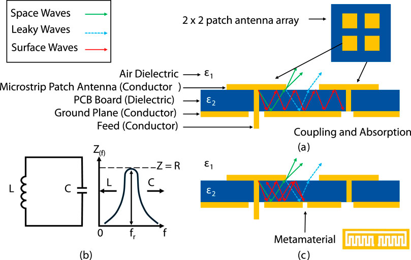
Figure 1. (a) Surface wave coupling and absorption by adjacent elements. (b) Equivalent inductive (L) and capacitive (C) resonator circuit model of the ML-CSRR with impedance (Z) vs. frequency (f) showing the resonance frequency (fr). (c) Integration of the ML-CSRR into the ground plane, suppressing surface wave coupling and preventing absorption by neighboring elements.
At the resonance frequency (fr), the impedance of a parallel LC resonator has peak resistance, and no reactance as capacitive and inductive reactances cancel.
When this occurs according to Equation 1, if the terminal impedance (ZT) from the resonator is much greater than the characteristic impedance (Z0), the reflection coefficient (Γ) becomes approximately 1. This implies a total reflection without a phase change that would lead to power loss (Pozar, 2012).
Engineered properly, a MTM can increase the isolation of closely spaced elements and allow for a miniaturized array with enhanced performance. In this study, ML-CSRRs incorporated on the ground plane between array elements point symmetrically between array elements as coupling is dominated by diagonal elements due to the locations of the feed pins for the proposed unit cell. This configuration minimizes the number of ML-CSRRs required and provides a simple and repeatable design process. Figures 1a, c give a qualitative depiction of the propagation of surface waves between closely spaced elements with and without a MTM resonator.
As a part of this study, the coupling of a simple standard 2 × 2 array and 2 × 2 MMA at a center frequency of 5.8 GHz and an element spacing of 2 mm were simulated using HFSS. Additionally, a conventional array with an element spacing of half a wavelength was simulated. The results of these simulations are depicted in Figure 2 and show more than 3 dB decoupling achieved as compared to the closely spaced array with no meander lines; however, there is still potential for improvement and optimization, as shown by the conventional array results.
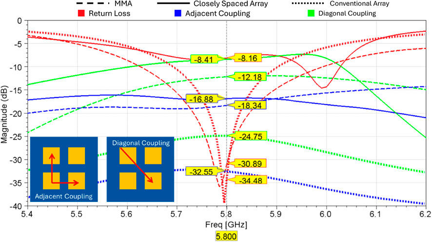
Figure 2. Results of the simulation of a closely spaced 2-mm element spacing array (solid lines), MMA with a 2-mm element spacing (dashed), and conventional (∼λ/2) reference array (short dash) with a center frequency of 5.8 GHz, showing that the MMA shows more than a 3-dB improvement in diagonal coupling compared to the closely spaced array.
Another consideration in determining the pitch between array elements is obtaining a desirable radiation pattern. Standard MPA arrays are commonly designed with an element separation of λ/2 to shape a broadside radiation pattern. However, the new design does not use this conventional λ/2 spacing, and thus the propagated waves do not constructively interfere at the broadside of the array, degrading the pattern shape, directivity, and gain. To mitigate this, array elements are sequentially phase-fed to shape a broadside radiation pattern. This technique allows for an area-reduced 2 × 2 array that is polarization reconfigurable with a radiation pattern and gain like a single MPA with the addition of beam steering capabilities. Figure 3 depicts the phase feeding necessary to achieve different polarizations using a 2 × 2 MMA.
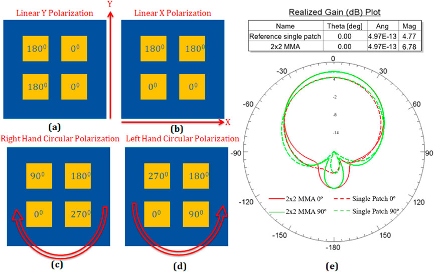
Figure 3. Sequential phase feeding of a 2 × 2 MMA (a) linear Y polarization; (b) linear X polarization; (c) right-hand circular polarization; (d) left-hand circular polarization, and (e) example radiation patterns in two orthogonal planes (0° in red and 90° in green). Solid lines correspond to the sequentially phase-fed 2 × 2 MMA, while dashed lines represent a single-element antenna. Note the similarity between the radiation patterns of the two antennas.
From the initial results, MMAs, with smaller dimensions, will have wider beam widths and reduced gain compared to standard arrays with the same number of elements; however, it is expected that with larger scaling, more elements will be able to fit into a given area, eventually allowing MMAs to achieve higher gain for a given area. Therefore, the 2 × 2 MMA is envisioned to become a foundational building block from which larger arrays can be designed for specific applications.
3 Material and fabrication considerations
Prior to designing and simulating the reference arrays and MMAs, careful consideration was given to material and fabrication possibilities. Initially, an optimized 4-layer stack-up configuration with Rogers 5,880 as the substrate was selected due to the low values of the loss tangent (tan (δ)) and dielectric constant (Dk). However, the complexity and cost of manufacturing using Rogers 5,880 facilitated the decision to use FR4.
FR4 is an industry-standard glass-reinforced epoxy laminate which is cost-effective, widely available, and simpler to manufacture. Despite the advantages, FR4 has a significantly higher loss tangent and dielectric constant compared to Rogers 5,880. Calculations of the losses in 50-Ω microstrip transmission lines for both FR4 (Dk = 4.4, tan(δ) = 0.02) and Rogers 5,880 (Dk = 2.2, tan(δ) = 0.0009) at 5.8 GHz with a copper (Cu) thickness of 17 µm and a conductor surface roughness of 1 µm calculated according to the Groiss model indicate a much higher attenuation (α) for FR4 (α = 0.024 dB/mm) than the Rogers substrate (α = 0.005 dB/mm).
While the higher Dk of FR4 results in more tightly coupled fields in the substrate, leading to reduced radiation losses, the increased tan (δ) dominates and increases transmission line loss. Consequently, a decrease in radiation efficiency is expected when using FR4 due to its larger Dk value. It is important to note that performance improvements are achievable with alternative materials. With the decision to use FR4, standard 4-layer stack-ups available from Sunstone Circuits were carefully evaluated. Trade-offs between antenna bandwidth, radiation efficiency, and feed line losses were considered by simulating MPAs in HFSS, using models such as that shown in Figure 4.
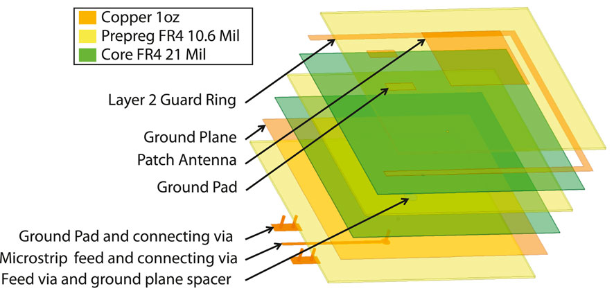
Figure 4. Diagram of test MPA design and 0.078″ stack up thicknesses.
Testing determined that Sunstone’s standard 1 oz, 0.078″FR4 4-layer stack-up provided acceptable trade-offs. The layer structure is shown in Figure 4. The top metal layer was used to define the radiating patch elements, while the second layer beneath the patches was left empty to provide a thicker dielectric layer, thereby improving bandwidth (BW) and radiation efficiency. Because fabrication rules do not allow a completely empty copper layer, a guard ring was included on this layer but placed far enough from the radiators to avoid impacting antenna performance. The third metal layer served as a ground plane for both the feed structures and radiating elements, and the fourth layer, containing the feed lines, was positioned closer to the ground plane than the radiators to confine fields within the dielectric and minimize spurious radiation losses.
Following this, the HFSS design was converted into Gerber and NC drill files using Altium Designer and sent to Sunstone Circuits for fabrication. To achieve this, the HFSS model was exported as a .dxf file and imported into Altium Designer. The .dxf file will only transfer the physical contours of the HFSS model, requiring modification in Altium Designer to match the original design. While the .dxf import usually maintains the same dimensional units as in HFSS, this needs to be verified. PCB manufacturers require both Gerber and NC drill files: the Gerber file provides the design layout by layer, and the NC drill file specifies drill locations such as vias. These files are generated via the “Fabrication Output” tab in the Altium Designer PCB file menu. The test MPA in Figure 5 performed in good agreement with the simulated results, indicating that the materials and fabrication processes were sufficient to proceed with the design of the reference MPA arrays and MMAs.
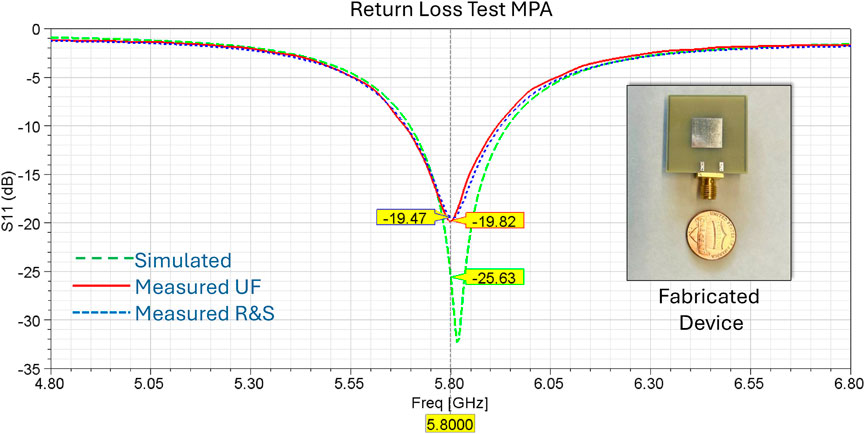
Figure 5. Return loss of test MPA structure; the inset shows the image of fabricated MPA.
4 Design and simulation
The MMAs were designed and simulated by independently creating and optimizing the ML-CSRRs, feedlines, and arrays before integrating them into a single model for final optimization. This approach ensures a simple and repeatable design process. The feedlines were first designed in the ADS schematic environment to generate an initial layout, which was then transferred to HFSS for full-wave simulation and optimization. Complete arrays with feeding structures were subsequently simulated in HFSS.
4.1 Design of the ML-CSRR
Based on the basic parallel circuit model of ML-CSRRs, a straightforward design model was developed to engineer the resonance frequency of the ML-CSRR. Figure 6 shows the HFSS model and final dimensions used to obtain the targeted 5.8 GHz resonance frequency.
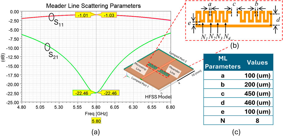
Figure 6. (a) ML-CSRR scattering parameters with model inset; (b) ML-CSRR design and parameters; (c) parameter values.
The model features a microstrip transmission line between two ports, with the ML-CSRR centered between the ports and located on the ground plane. At resonance, the maximum return loss and minimum insertion loss are observed using scattering parameters. Using this approach, the ML-CSRR structure may be tuned to any frequency of interest.
Each parameter in the figure influences the resonant frequency of the ML-CSRR, and this was explored using the model shown. Increasing the ML gap (a) length shifts the frequency lower, as does increasing the gap (c), though with an exceedingly small effect. A larger ML width (d) or a wider ML (b) also lowers the resonant frequency. Additionally, a wider gap widthwise (e) slightly reduces the frequency. The number of meanders (N) inversely affects the frequency when other parameters are constant; for example, an 8-N configuration will have a higher frequency than a 10-N or 12-N setup. However, when the total length and width of the ML-CSRR are maintained across different N values, lower N values result in higher frequencies, highlighting the flexibility in designing ML-CSRRs using these parameters.
4.2 Design of the MMA feedlines
Due to the close spacing of array elements, ML-CSRRs—which if not considered, will negatively affect the feed network by reflecting power back to the source—and sequential phase feeding requirements, a unique feed network must be designed.
The feed network is designed using three concepts: quarter-wave transformers, equal power splitting, and phase control by offset electrical lengths. The input impedance (Z0) and terminal impedances were designed for 50 Ω; for simplicity and practicality, a linear polarization with a 0° and 180° sequential phase offset was used. Because the radiating elements are closely spaced, their radiated waves interfere and distort the radiation pattern. As discussed, to overcome this challenge and obtain a desirable radiation, sequential phase feeding was used (Figure 3). Figure 7 illustrates the dimensions, scattering parameters, and phase at the output ports for the 2 × 2 and 4 × 4 feed networks.
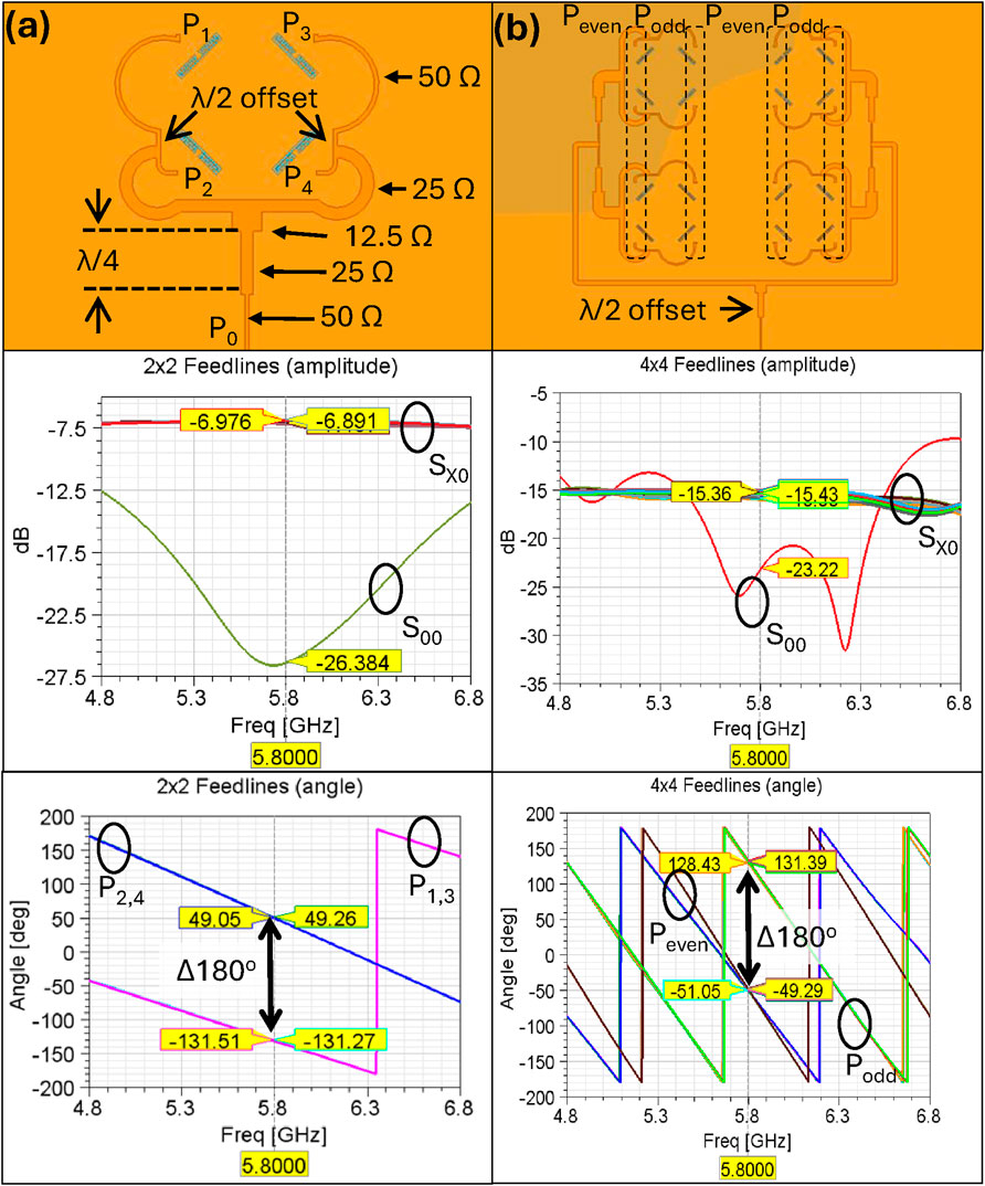
Figure 7. From top to bottom, designed microstrip feedlines, insertion and return losses of feedlines, and output port phases referenced to the input port (P0) for (a) the 2 × 2 MMA and (b) the 4 × 4 MMA.
The vias that feed the individual elements need not be excessively evaluated due to the via length being much less than the guided wavelength, which minimizes this via’s impact on performance.
As the MMAs scale up, designing the feed networks becomes increasingly complex due to losses from transmission lengths, limited area, and phase issues in closely spaced adjacent lines. For the 16-element MMA, this required greater 2 × 2 unit-cell spacing, and for a 64-element MMA, obtaining acceptable performance was ruled impractical. Larger arrays require alternative feed networks, such as multilayer architectures. A multilayer feed network was not used due to the standing waves and resonant cavities inherent in multiple layer designs. The cavities in the substrates sandwiched between two ground planes are fed by the via that connects the feed network to the array elements and lead to lower efficiencies. To overcome these designs, the use of via fences made of blind via around the feed via and other suppression methods are commonplace; however, these add significant manufacturing complexities and costs. Alternative feed architectures, such as coaxial feeding, were also rejected along similar lines.
4.3 Designing the MMAs
Standard 2 × 2, 4 × 4, and 8 × 8 reference MPA arrays were designed and simulated using coaxial feeds with a center frequency of 5.8 GHz and a free space wavelength of approximately 52 mm. The MPA dimensions of the reference arrays were used with the designed MMA feeding networks and ML-CSRRs to design the complete MMAs. For a 2 × 2 MMA unit cell, the spacing between elements was reduced to 3 mm (∼λ/16), compared to 25.8 mm (∼λ/2) for the reference arrays. For the 16-element MMA, the unit cell spacing was 3 mm (∼λ/16); however, the spacing between cells was 13 mm due to constraints introduced by the feed network. Adjusting the spacing between MMA unit cells provides additional design flexibility, allowing some trade between realized gain and area reduction. This and the scalability of size reduction were explored by simulating the reference and MMAs using ideal coaxial feeding; results from these simulations are presented in Table 1.
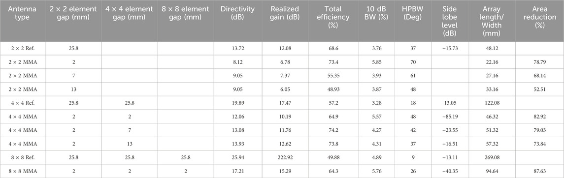
Table 1. Figures of merit for simulated reference and MMAS using ideal coaxial feeding.
From the results, the area reduction scales with the increase in array elements, and it is expected that in large arrays, there will be a crossover point in which greater gain may be obtained within reduced areas. Additionally, total efficiency has a complex dependence on the antenna configuration, where achieving the best performance requires optimizing element spacing and, in some cases, making size trade-offs. In all evaluated cases, the MMAs outperform their corresponding reference arrays. Regarding side-lobe levels (SLL) and 10 dB BW, results show that MMA arrays with smaller element spacing exhibit lower SLLs and broader BW, both of which are generally desirable characteristics for antenna arrays. Note that the area of each array was measured from the outermost corners of the outermost patches. After these simulations, the incorporation of the feed networks and subsequent optimization occurred. Finally, simulations that incorporated SMA connectors as inputs into the array were performed to confirm acceptable performance. To quantify the effects of the ML-CSRR, closely spaced 2 × 2 and 4 × 4 arrays without ML-CSRR were also simulated. Table 2 shows the results of these simulations.
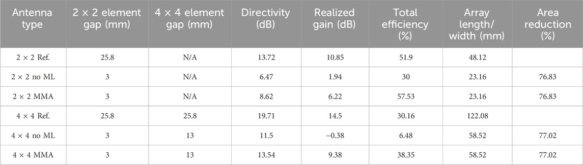
Table 2. Figures of merit for reference and MMAS with feeding networks and SMA incorporated.
Following these, the steps outlined in Section 3 were completed, and the devices shown in Figure 8 were received.
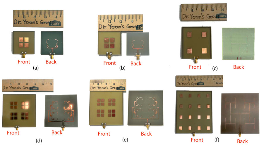
Figure 8. Front and back views of the manufactured arrays: (a) 2 × 2 MMA; (b) 2 × 2 closely spaced array without ML; (c) 2 × 2 reference array; (d) 4 × 4 MMA; (e) 4 × 4 closely spaced array without ML; (f) 4 × 4 reference array.
During inspection of the fabricated devices, the ML dimensions were examined by exposing the ground layer and measuring them optically with a calibrated Olympus BX-51 microscope. Compared to the designed ML discussed earlier, the fabricated structures exhibited deviations of up to ∼11% (Figure 9).
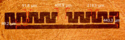
Figure 9. Image of fabricated ML on ground plane with measured dimensions.
This deviation was considered acceptable, as Monte Carlo simulations performed for the ML prior to fabrication accounted for dimensional tolerances of ±20%. The observed variations did not significantly degrade antenna performance, as shown in the following section.
5 Measurement methods and results
With the designs fabricated, the reference and MMAs were measured at the University of Florida and the Rohde and Schwarz facility in Dallas, Texas. Images of the measurement setups are shown in Figure 10.
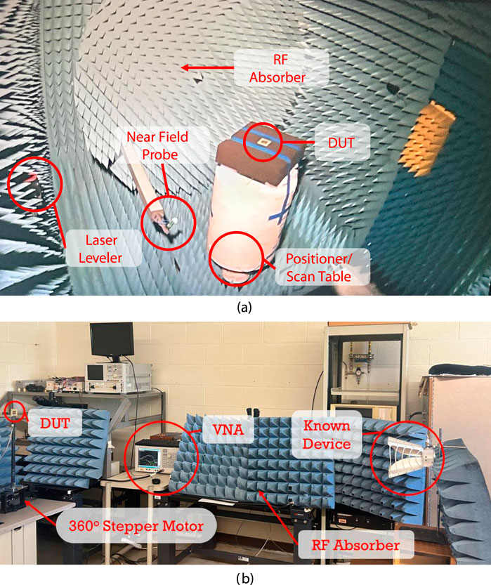
Figure 10. Antenna measurement setups: (a) Rohde and Schwarz (b) University of Florida.
To calibrate the near-field measurement setup in Figure 10a, a known antenna was used as a transmitter (Tx) and was measured by the near-field probe. These measurements were compared to the known values, and adjustments were made to calibrate the measurement set up. After calibration, near-field measurements of the DUT were taken by rotating the near-field probe around the Tx as the scan table rotates in steps. In this way, a three-dimensional measurement could be conducted efficiently. After the near-field measurements were complete, the return loss of the DUT was measured and used with near-field measurement data to algorithmically approximate the far-field characteristics.
The setup shown in Figure 10b uses a known antenna as the Rx and the DUT as the Tx, but the Tx and Rx are placed at a distance greater than the Fraunhofer distance.
(D) is the largest dimension of either the Rx or Tx antenna’s aperture, and (λ) is the free space wavelength of the frequency of interest. With the Tx and Rx positioned, the stage was rotated by a stepper motor with 3,200 steps per rotation, providing an accuracy of approximately 0.11°. Since the system is not yet automated, measurements were recorded using a vector network analyzer (VNA) at 10° intervals for each measured plane. The VNA was calibrated manually using a short-open-load-through (SOLT) method and kit. The insertion loss (S21) was then converted into realized gain using
—where the realized gain (
The method used in this study is referred to as the “substitution method”; however, this method is not without its limitations and uncertainties. This includes errors due to the positioning and alignment of radiators for proper measurement of power amplitude and polarization matching. Additionally, the quality of the known device and the calibration of the reference planes are of particular importance as any errors occurring here will be directly seen in the measured DUTs’ gain. Finally, it is readily apparent from Figure 10b that measurements were not performed in anechoic conditions, which is another source of uncertainty, other than the method used. This will lead to multipath issues including reflections and scattering of radiated fields, leading to the receiver sensing the results of the interference of these fields and direct line-of-sight fields, and the reception of other fields in the environment such as Wi-Fi operating near our measured device’s operating frequency.
After setup verification and calibration procedures, measurements of the DUT were conducted, with tabulated measurement results are given in Table 3. The simulated and measured results indicate that MMAs with 2N elements have a similar half-power beamwidth (HPBW) and peak realized gain as a reference array with 2N−1 elements.
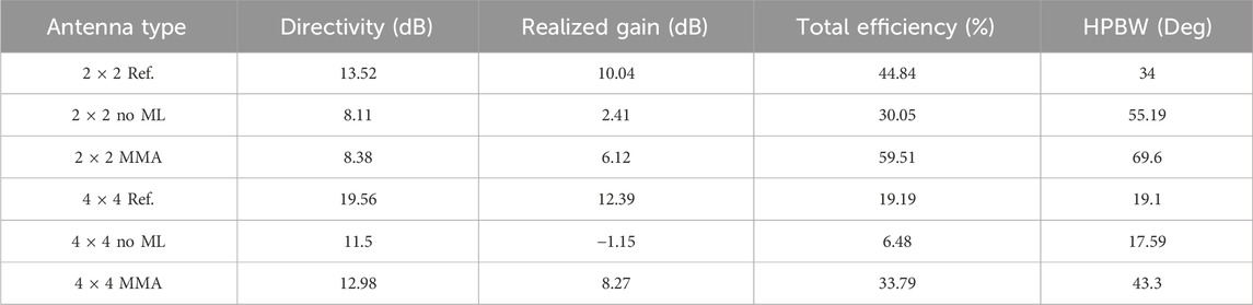
Table 3. Measured results for reference and MMAS.
These results demonstrate that both the reference arrays and MMAs and closely spaced arrays without MLs closely match the simulated performances. Some shifts in the measured results are observed due to non-ideal material characteristics and fabrication tolerances, particularly the dimensional tolerance of 20% for the etching of the ML-CSRR by the manufacturer (discussed in Section 4). Graphical results for measured arrays are shown in Figures 11, 12. These results show that the simulations and measurements from both the University of Florida and Rohde and Schwarz closely agree, further confirming the results.
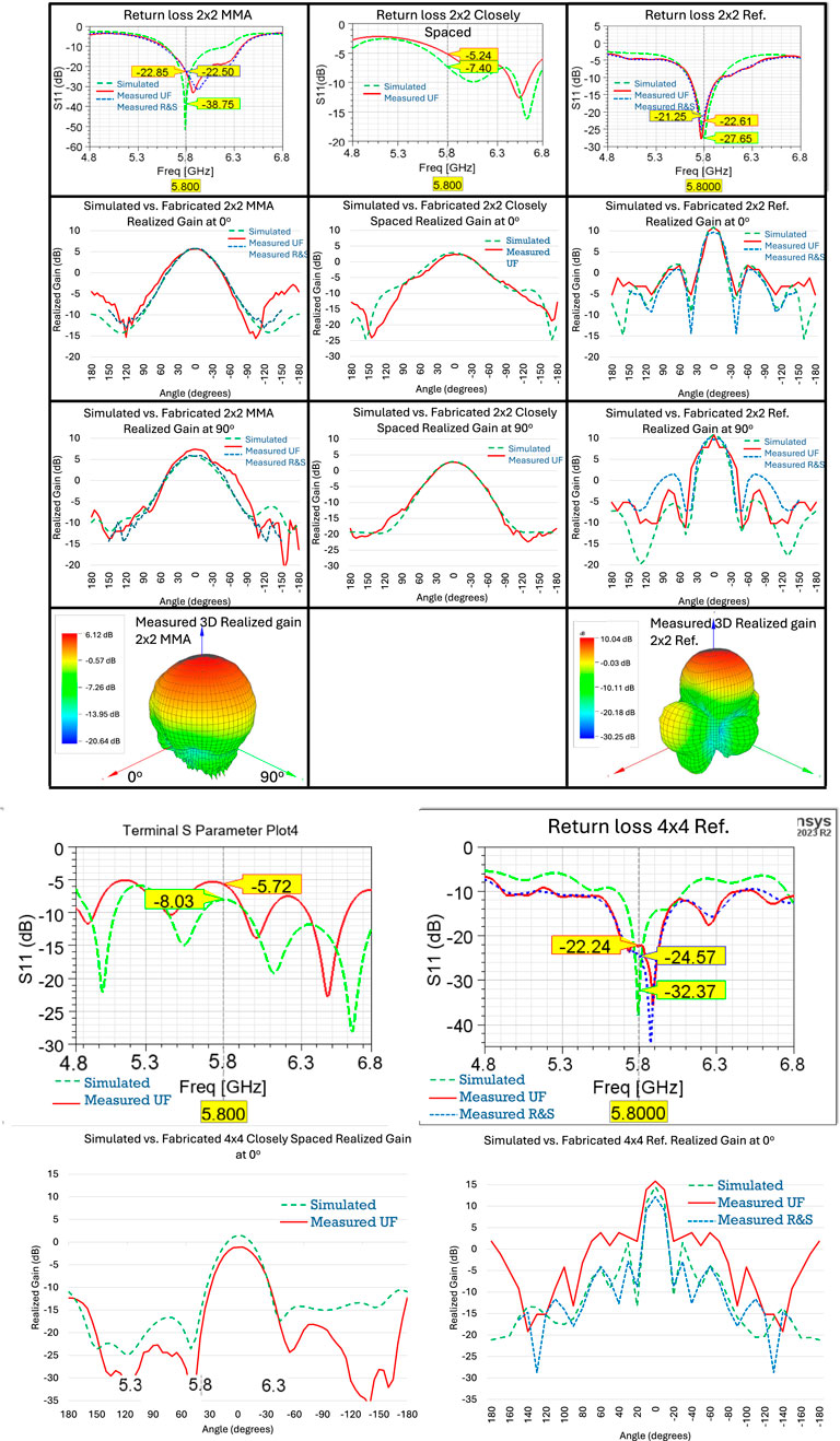
Figure 11. Comparison of three 2 × 2 MMAs. Left: 4 × 4 MMA with ML. Center: 2 × 2 closely spaced array without ML. Right: reference 2 × 2 array. From top to bottom: return loss, realized gain at 0°, realized gain at 90°, and 3D realized gain radiation pattern.
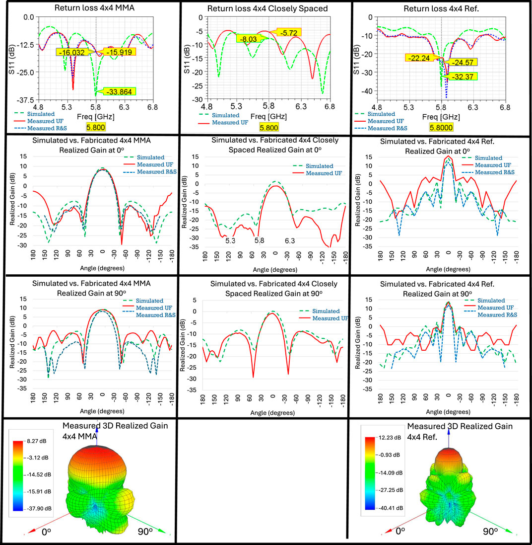
Figure 12. Comparison of three 4 × 4 MMAs. Left: 4 × 4 MMA with ML. Center: 4 × 4 closely spaced array without ML. Right: reference 4 × 4 array. From top to bottom: return loss, realized gain at 0°, realized gain at 90°, and 3D realized gain radiation pattern.
6 Conclusion
This study introduced a scalable ML-CSRR enabled-method for miniaturizing MPA arrays for SWaP-constrained applications and validated up to 4 × 4 (16-element) arrays with fabrication and simulations, indicating potential for further scaling. By incorporating ML-CSRRs into the ground plane, we achieved substantial improvements in isolation between closely spaced elements, allowing for reduced spacing while maintaining acceptable radiation patterns. Simulations of compact MMA prototypes showed an over-3 dB improvement in diagonal coupling compared to standard reference arrays. Despite some trade-offs, such as wider beam widths and reduced gain, the potential for higher element densities in MMAs suggests that compact designs with comparable antenna characteristics are achievable. Although using FR4 material introduced some performance limitations compared to Rogers 5,880, the prototypes closely matched simulated performances. Simulations demonstrated that compared to reference designs, MMAs achieved higher total efficiency prior to feedline integration, reduced SLLs, and increased 10 dB BWs. Measurements by multiple parties confirmed that MMAs with reduced dimensions achieve expected radiation characteristics and performance, validating their suitability for applications that require both large arrays and miniaturization. Overall, the proposed approach effectively addresses the challenges of minimizing element spacing and maintaining desired radiation characteristics, advancing compact antenna technology for SWaP-constrained environments.
Data availability statement
The raw data supporting the conclusions of this article will be made available by the authors, without undue reservation.
Author contributions
AW: Conceptualization, Data curation, Formal Analysis, Investigation, Methodology, Software, Validation, Writing – original draft, Writing – review and editing. AD: Conceptualization, Data curation, Formal Analysis, Investigation, Methodology, Software, Validation, Writing – original draft, Writing – review and editing. Y-KY: Funding acquisition, Project administration, Resources, Supervision, Writing – review and editing.
Funding
The author(s) declare that financial support was received for the research and/or publication of this article. This study was funded in part from the Cisco University Research Program Fund, a corporate advised fund of the Silicon Valley Community Foundation (Gift #2022-246616 (3696)), the NSF Convergence Accelerator Program (ITE-2235978), and the NSF Engine Program (2315320) (Corresponding author: Y-KY). These funders were not involved in the study design, collection, analysis, interpretation of data, the writing of this article, or the decision to submit it for publication. This study also received financial support from the Air Force Research Laboratory (AFRL) through a subcontractor of Mosaic Microsystems (DoD SBIR 2022.2: Air Force Phase II F2D-5021) as well as technical advice, mentorship, and guidance.
Acknowledgements
The authors extend their gratitude for the invaluable support and mentorship provided by these organizations, which have been essential to the success of this project and also recognize Rhodes and Schwarz for their technical advice, use of measurement facilities, and mentorship without financial support.
Conflict of interest
The authors declare that the research was conducted in the absence of any commercial or financial relationships that could be construed as a potential conflict of interest.
Generative AI statement
The author(s) declare that Generative AI was used in the creation of this manuscript. The authors verify and take full responsibility for the use of generative AI in preparing this manuscript. Specifically, QuillBot was used for grammar refinement and editing, and ChatGPT was used to improve the clarity and readability of the text.
Any alternative text (alt text) provided alongside figures in this article has been generated by Frontiers with the support of artificial intelligence and reasonable efforts have been made to ensure accuracy, including review by the authors wherever possible. If you identify any issues, please contact us.
Publisher’s note
All claims expressed in this article are solely those of the authors and do not necessarily represent those of their affiliated organizations, or those of the publisher, the editors and the reviewers. Any product that may be evaluated in this article, or claim that may be made by its manufacturer, is not guaranteed or endorsed by the publisher.
References
Balanis, C. A. (2016). Antenna theory: analysis and design. Fourth edition. Hoboken, New Jersey: Wiley.
Cho, H., and Yoon, Y. K. (2021). “Parallelly and diagonally placed meander-line slot resonators for mutual coupling reduction in a 2x2 patch array antenna,” in 2021 IEEE 21st Annual Wireless and Microwave Technology Conference (WAMICON), Sand Key, FL, USA, 28-29 April 2021, 1–5. doi:10.1109/WAMICON47156.2021.9443610
Choi, S. I., Lee, W., and Yoon, Y. K. (2022). “Compact frequency reconfigurable array antenna based on diagonally placed meander-line decouplers and PIN diodes for multi-range wireless communications,” in 2022 IEEE 72nd Electronic Components and Technology Conference (ECTC), San Diego, CA, USA, 31 May 2022 - 03 June 2022 (IEEE), 98–102. doi:10.1109/ECTC51906.2022.00025
Hwangbo, S., Yang, H. Y., and Yoon, Y.-K. (2017). Mutual coupling reduction using micromachined complementary meander-line slots for a patch array antenna. IEEE Antennas Wirel. Propag. Lett. 16, 1667–1670. doi:10.1109/LAWP.2017.2663114
Jang, H., Pahlavan, P., and Yoon, Y.-K. (2023). “Highly compact and high gain 2 x 2 patch array antenna with slotted meanderline Loading,” in 2023 IEEE 73rd Electronic Components and Technology Conference (ECTC), Orlando, FL, USA, 30 May 2023 - 02 June 2023 (IEEE), 1917–1920. doi:10.1109/ECTC51909.2023.00329
Khan, M. U., Sharawi, M. S., and Mittra, R. (2015). Microstrip patch antenna miniaturisation techniques: a review. IET Microwaves, Antennas and Propag. 9 (9), 913–922. doi:10.1049/iet-map.2014.0602
Pahlavan, P., Choi, S.-I., Wilcher, A., Kim, H.-I., Jang, H., and Yoon, Y.-K. (2023). “Metamaterial Based Compact Patch Antenna Array for Antenna-in-Package Solutions in Frequency Handover Applications,” in 2023 IEEE 73rd Electronic Components and Technology Conference (ECTC), Orlando, FL, United States: IEEE, 475–480. doi:10.1109/ECTC51909.2023.00085
Qamar, Z., and Park, H. C. (2014). Compact waveguided metamaterials for suppression of mutual coupling in microstrip array. Prog. Electromagn. Res. 149, 183–192. doi:10.2528/PIER14063002
Sun, L., Li, Y., and Zhang, Z. (2021). Decoupling between extremely closely spaced patch antennas by mode cancellation method. IEEE Trans. Antennas Propag. 69 (6), 3074–3083. doi:10.1109/TAP.2020.3030922
Keywords: array antenna, patch antenna, miniaturized antennas, polarization reconfigurable, defected ground structure, meander-line, electromagnetic band gap material, mutual coupling reduction
Citation: Wilcher A, David Cerpa A and Yoon Y-K (2025) Scalable metamaterial antenna arrays with suppressed mutual coupling for compact platforms. Front. Antennas Propag. 3:1695439. doi: 10.3389/fanpr.2025.1695439
Received: 29 August 2025; Accepted: 15 October 2025;
Published: 12 November 2025.
Edited by:
Shah Nawaz Burokur, Université Paris Nanterre, FranceReviewed by:
Seyed Ramin Emadian, Urmia University Urmia Lake Research Institute, IranAnitha V. R, BMS Institute of Technology, India
Copyright © 2025 Wilcher, David Cerpa and Yoon. This is an open-access article distributed under the terms of the Creative Commons Attribution License (CC BY). The use, distribution or reproduction in other forums is permitted, provided the original author(s) and the copyright owner(s) are credited and that the original publication in this journal is cited, in accordance with accepted academic practice. No use, distribution or reproduction is permitted which does not comply with these terms.
*Correspondence: Yong-Kyu Yoon, eWt5b29uQGVjZS51ZmwuZWR1