 Yingbo Liu
 Haiou Li1*
 Yuxiang Hao
- 1Guangxi Key Laboratory of Precision Navigation Technology and Application, Guilin University of Electronic Technology, Guilin, China
- 2The 34th Research Institute of China Electronics Technology Group Corporation, Guilin, China
Electro-optic modulators with low driving voltage and wide bandwidth are critical for advanced analog and digital communication systems. To achieve high-speed thin-film lithium niobate (TFLN) electro-optic modulators on silicon substrates, this work proposes a hybrid-loaded T type-U type traveling-wave electrode structure (TU-TWEs). The core of TU-TWEs in the introduction of an inductance compensation mechanism, which can effectively reduce the microwave refractive index and weaken the “slow light” effect, thereby matching the group velocity of light with the microwave velocity. We demonstrate a high-speed TFLN electro-optic modulator on a silicon substrate, with an electro-optic bandwidth greater than 110 GHz and a half-wave voltage of 1.35 V.
1 Introduction
The exponential growth of information technology has intensified the need for high-speed data transmission. Electro-optic modulators, being pivotal components for electrical-to-optical signal conversion in optical communications, and its performance enhancement is crucial for the realisation of high-speed and high-capacity optical communication systems (Winzer et al., 2018; Qi and Li, 2020) Nevertheless, traditional bulk lithium niobate modulators face limitations in size and integration level, failing to meet the dual demands of miniaturization and high performance in contemporary optical interconnection systems. TFLN renowned for its superior electro-optic effects, has emerged as a highly promising material for electro-optic modulator applications in recent years. The development of TFLN electro-optic modulators primarily focused on process exploration before 2018, where the maturity of etching and bonding techniques critically deter-mined device performance and stability (Rao et al., 2016; Hsu et al., 2017).
Marko Lončar’s team pioneered a CMOS-compatible TFLN electro-optic modulator in 2018 (Wang et al., 2018), achieving integrated devices with low half-wave voltage (Vπ) and high modulation efficiency through optimized etching and bonding processes. This mile-stone signified the evolution of TFLN modulators from process exploration to application development, laying the groundwork for future advancements. Nevertheless, conventional coplanar waveguide (CPW) electrode designs encounter critical limitations: high microwave losses, limited electro-optic bandwidth, and the mismatch be-tween microwave and optical group velocities is particularly prominent (Liu Y. et al., 2021). In response to this challenge, Mian Zhang et al. introduced a periodically loaded T-shaped micro-structured electrode design in 2021 (Kharel et al., 2021). mitigating microwave losses via in-creased electrode spacing while enhancing velocity matching through capacitive compensation strategies. Although this design achieved optimal microwave-optical velocity matching on quartz substrates, its primary constraint stems from substrate material limitations. The slow-light effect inherent to T-shaped electrodes substantially increases microwave refractive indices, rendering velocity matching unattainable on silicon substrates. Despite the advantages of low microwave loss with quartz substrates, challenges including prohibitive cost, mechanical fragility, and incompatibility with standard processes hinder their adoption for large-scale integration. Consequently, realizing effective microwave refractive index and optical group index matching on silicon substrates emerges as a pivotal challenge in developing low-cost, high-reliability TFLN modulators.
Present research into silicon-based group velocity matching concentrate on three principal approaches: 1. Silicon substrate etching: Reducing the equivalent microwave refractive index of silicon substrates through undercut etching (Chen et al., 2022) or backside etching (Wang M. et al., 2024). However, these methods rely on complex micro-nanofabrication processes with low process tolerance, inducing mechanical stress and waveguide distortions that degrade device yield.2. Optical delay tuning: Adjusting the effective refractive index of optical waves through waveguide design or phase compensation structures, such as the path delay design employed in cross-waveguide phase modulators (Du et al., 2024). While this approach avoids substrate etching, it requires precise control of optical path differences, features high design complexity, and tends to introduce addition-al insertion losses, making it unsuitable for mass production.3. Cascaded fast-slow wave electrodes (Wang S. Y. et al., 2024): This approach achieves equivalent group velocity matching through proportional adjustments, leveraging the alternating configuration of fast and slow wave traveling electrodes. This method has the potential for flexible design and process compatibility, but the issues of impedance matching and microwave reflection suppression need to be solved.
In summary, although implementing high-speed modulation on silicon substrates offers significant advantages, this process inevitably faces challenges including insufficient mechanical reliability, elevated optical losses, and etching difficulties. In response to these challenges, we propose a TFLN electro-optic modulator featuring a TU-TWEs. The design’s cornerstone is an inductive compensation mechanism that suppresses microwave refractive indices, alleviates “slow light” effects, and successfully enables optical group velocity-microwave velocity matching on silicon substrates, consequently enabling high electro-optic bandwidth. Through simulation verification, when the modulator length is
2 Principle of electro-optical modulators
The thin-film lithium niobate (TFLN) electro - optic modulator with a TU-TWEs proposed in this paper is composed of an optical part and an electrical part. The optical subsystem employs a Mach-Zehnder interferometer (MZI) configuration incorporating two multimode interference (MMI) splitters and parallel-aligned TFLN ridge waveguides. Input light is equally split into two coherent beams through the input MMI splitter, propagating through symmetrically arranged lithium niobate waveguides. TFLN’s pronounced electro-optic effect exhibits linear dependence of effective refractive index on external electric fields, enabling dynamic phase modulation of optical waves. Specifically, equal-magnitude counter-directional electric fields generated across vertical electrode gaps create
Where
The half-wave voltage (
Where
The three key factors limiting the bandwidth of the modulator are: (1) impedance matching; (2) microwave loss, primarily absorbed by the traveling waveguide and the silicon substrate; and (3) matching the group velocity of light with the microwave signal velocity.
1. Characteristic impedance matching refers to the state where the source impedance, transmission line characteristic impedance, and load impedance achieve equality. Impedance mismatch causes signal reflections at discontinuities along transmission lines, sending partial signals back to the source. Such reflections lead to signal attenuation and introduce interference, degrading overall signal quality.
2. Conductor loss is one of the primary losses in microwave transmission, mainly caused by the finite conductivity of metals. When current flows through metals, resistive losses occur due to inherent resistance. The height of metallic electrodes influences current flow paths and distribution patterns. High-frequency operation accentuates skin effect phenomena, confining current within the conductor’s surface layer. When electrode thickness falls below the skin depth threshold, current confinement to di-minished cross-sections increased resistive losses. Electrode height also affects electric field distribution within transmission lines. Improper electrode height may cause electric field leakage or radiation into unintended regions, generating additional radiative losses.
3. In traveling-wave electro-optic modulators, light propagates through lithium niobate waveguides while microwave signals travel along microwave guides. Mismatched group and phase velocities prevent uniform voltage modulation along the waveguide. At high modulation frequencies, this velocity mis-match introduces phase errors that degrade modulation performance.
Capacitively loaded traveling-wave electrodes (CL-TWEs) have been demonstrated to enhance electro-optic modulation bandwidth in TFLN electro-optic modulators (Nelan et al., 2022). The bandwidth improvement mechanism of CL-TWEs originates from two synergistic effects: 1) The T-type electrode enlarges inter-electrode spacing, mitigating current crowding effects and lowering microwave propagation losses. This design strategy is crucial for reducing the energy dissipation during the transmission process and helps to improve the overall performance and bandwidth of the modulator. 2) When implemented on quartz substrates, CL-TWEs simultaneously satisfy microwave-optical velocity synchronization and
3 Design and simulation
Figure 1a illustrates the cross-sectional structure of the modulator, comprising a 500
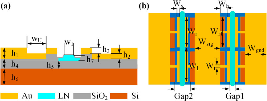
Figure 1. Schematic diagrams of the periodically hybrid-loaded T type-U type traveling-wave electrode structure TFLN electro-optic modulator: (a) Cross-section of the modulator,
3.1 Analysis of transmission line equivalent circuit model
The transmission line equivalent model of hybrid-loaded T type-U type travel-ing-wave electrode structure (TU-TWEs) is shown in Figure 2.
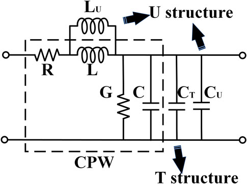
Figure 2. Equivalent circuit of hybrid-loaded T type-U type traveling-wave electrode structure (TU-TWEs).
Based on microwave theory, the characteristic impedance and propagation constant formulations derived from the equivalent transmission line model are given by Equations 5, 6 (Fang et al., 2023; Cheng et al., 2024):
Where
The microwave refractive index is formulated through the propagation constant Equation 9:
The equivalent inductance and capacitance extracted from Figure 2 model are expressed as Equations 10, 11:
The equivalent inductance equals the parallel combination of parasitic inductances from main and U-type electrodes, while the equivalent capacitance results from parallel parasitic capacitances of main, T-type, and U-type electrodes.
The U-type structure contributes only parasitic inductance without introducing parasitic capacitance. The velocity synchronization mechanism is achieved through: Compared to conventional CL-TWEs, the integrated U-type structure introduces parallel inductive loading that suppresses equivalent inductance, counterbalancing the microwave refractive index elevation induced by T-type capacitive loading. Although this design increases characteristic impedance as Equation 5, the impedance variation can be mitigated through optimized thickening of the underlying SiO2 layer (Li et al., 2024).
3.2 High frequency analysis of modulator
According to the above analysis, microwave loss is one of the critical factors limiting electro-optic bandwidth. The influence of modulator electrode height on device performance is analyzed via finite element method (FEM) simulations, calculating microwave losses at
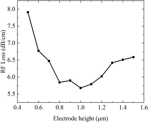
Figure 3. The trend of RFs Loss with the electrode height.
Through systematic analysis of U-type structure’s influence demonstrates that parametric tuning of
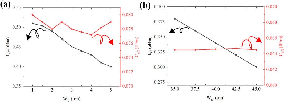
Figure 4. Dependence of equivalent circuit parameters with U-type structure: (a) Equivalent inductance and capacitance with
We conducted an in-depth analysis of the U-type structure’s effects on microwave refractive indices and radiofrequency attenuation characteristics. Simulation results in Figure 5 show that increasing
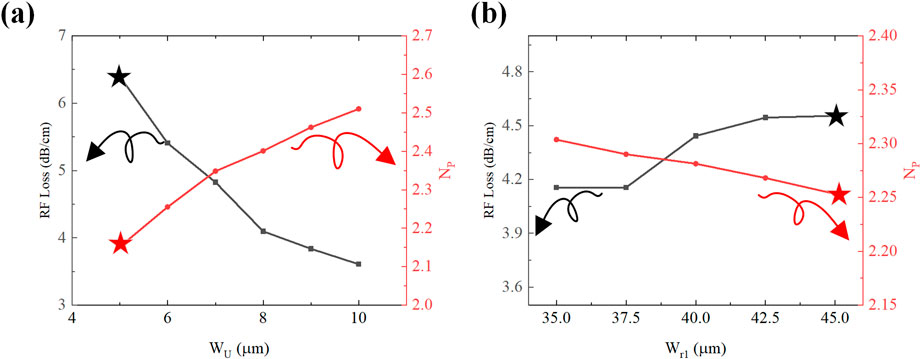
Figure 5. RF performance trends with U-type structure; (a) RF Loss and microwave refractive index trends with
While the T-type structure exhibits negligible impact on equivalent inductance, it substantially modulates equivalent capacitance values (Liu X. C. et al., 2021). The following analysis focuses on the effects of parameters
We conducted systematic parametric analysis of
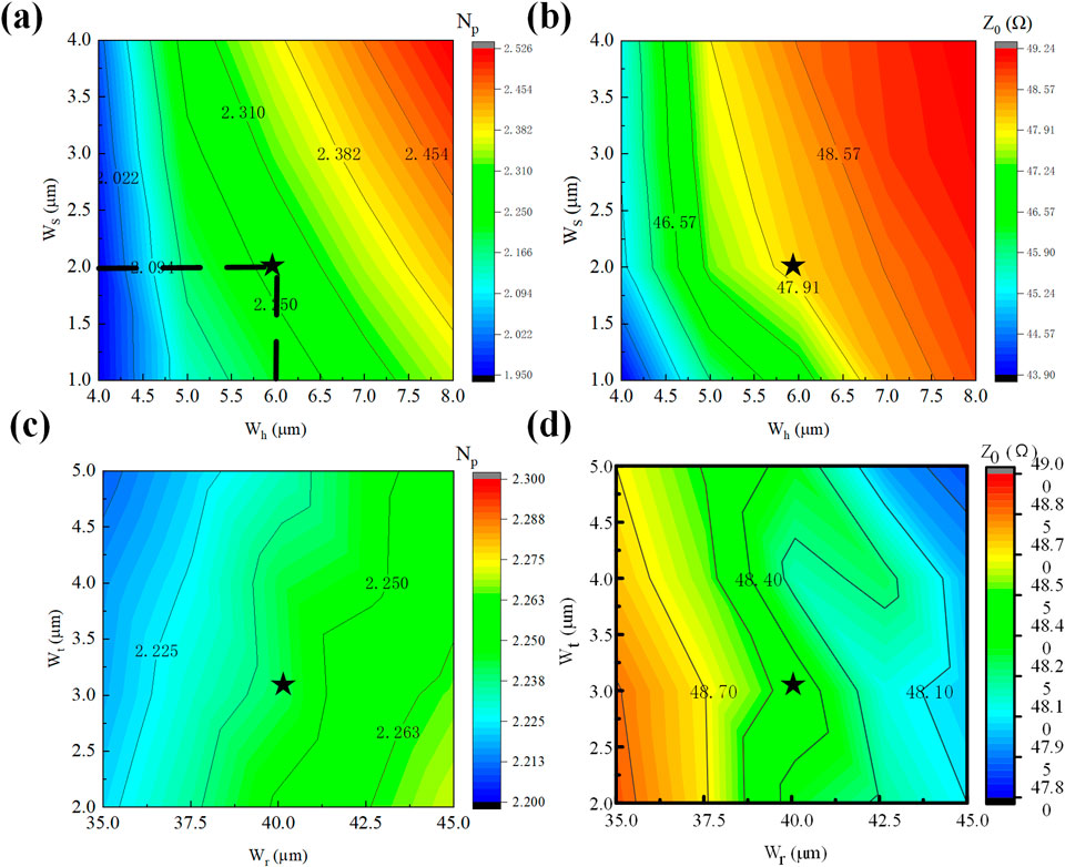
Figure 6. Trend of RF performance with T-type structure parameters
Experimental investigations reveal limited parametric influence on overall device characteristics. Figures 6c,d displays contour mapping results obtained through comprehensive parametric optimization. Increasing
3.3 Influence on modulation efficiency
Key determinants of electro-optic conversion efficiency include waveguide effective refractive index and electro-optic field overlap factor. Effective refractive index is governed by geometric parameters of the ridge waveguide, specifically ridge width and, etch depth. For defined waveguide architectures and operating wavelengths, the
Guided by the theoretical framework of the half-wave voltage-length product Equation 5, numerical simulations of the modulator’s optical mode field and electro-static field were conducted using finite element analysis software. The optical mode electric field distribution is depicted in Figure 7a, and the electrostatic field distribution is presented in Figure 7b.
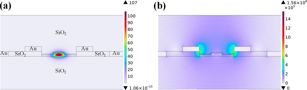
Figure 7. (a) TE mode optical field of the modulator. (b) Electrostatic field of the electrode.
In the T-type structure,
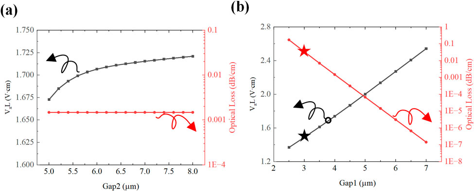
Figure 8. U-type structure and T-type structure electrode spacing on modulation efficiency (a) Trend of modulation efficiency and optical loss with U-type structure spacing
3.4 Electro-optic modulation bandwidth simulation
According to microwave transmission theory, the optical-electric transmission function can be expressed as Equation 12 (Jing et al., 2020):
The propagation loss
We performed a comprehensive finite-element analysis of the modulator’s performance. We specifically calculated its characteristic impedance, microwave loss, and microwave speed as key parameters. In this study, the modulator length was set to
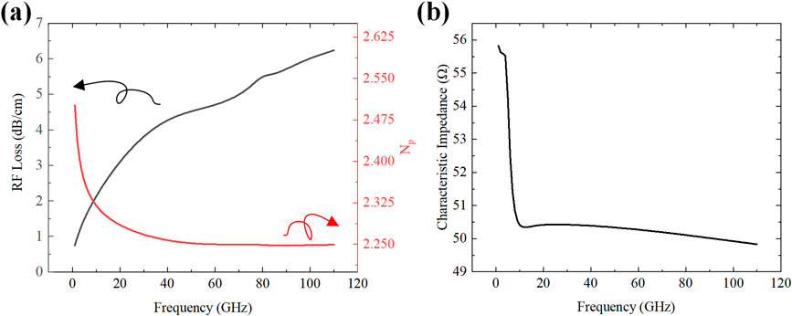
Figure 9. RF performance of the modulator (a) Frequency response of RF Loss and microwave refractive index. (b) Frequency response of characteristic impedance.
Finally, by substituting the calculated frequency-dependent microwave loss, refractive index, and characteristic impedance of the device into Equation 1, the electro-optic response shown in Figure 10 was obtained. Simulation results demonstrate a
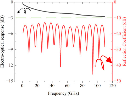
Figure 10. Electro-optic response and reflection coefficient of a
Through simulations and analysis, we demonstrated a thin-film lithium niobate electro-optic modulator chip with a half-wave voltage of
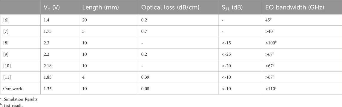
Table 1. Performance Comparison of LNOI MZI Modulator.
4 Conclusion
In this work, we present a high-speed TFLN electro-optic modulator on a silicon substrate that achieves a match between microwave velocity and optical group velocity. Specifically, we design and propose a TU-TWEs. The introduction of the U-type electrode in this structure effectively reduces the equivalent inductance of the transmission line without significantly affecting its equivalent capacitance. This unique inductance compensation mechanism helps to mitigate the “slow light” effect, enabling a good match between the optical group velocity and microwave velocity on a silicon substrate and significantly enhancing the electro-optic bandwidth. Simulation results show that when the modulator length is
Data availability statement
The original contributions presented in the study are included in the article/supplementary material, further inquiries can be directed to the corresponding author.
Author contributions
YiL: Methodology, Conceptualization, Writing – original draft, Writing – review and editing, Visualization, Formal Analysis, Validation. HoL: Resources, Funding acquisition, Validation, Writing – review and editing. YuL: Visualization, Writing – review and editing, Supervision. HsL: Project administration, Writing – review and editing, Software. YH: Writing – review and editing, Investigation. LQ: Writing – review and editing, Data curation. JY: Writing – review and editing, Data curation.
Funding
The author(s) declare that financial support was received for the research and/or publication of this article. This research was funded by National Natural Science Foundation of China (No. 62174041); Guangxi Science and Technology Plan Project (AD24010060); Guangxi Science and Technology Base and Talent Special Project (Guike AD24010060).
Acknowledgments
We thank the National Natural Science Foundation of China, the Guangxi Natural Science Foundation, the GUET Graduate Education Innovation Project for partial funding and the National Key R&D Program of China.
Conflict of interest
Authors YiL, YuL, HaL, YH, LQ, and JY were employed by The 34th Research Institute of China Electronics Technology Group Corporation
The remaining author declares that the research was conducted in the absence of any commercial or financial relationships that could be construed as a potential conflict of interest.
Generative AI statement
The author(s) declare that no Generative AI was used in the creation of this manuscript.
Publisher’s note
All claims expressed in this article are solely those of the authors and do not necessarily represent those of their affiliated organizations, or those of the publisher, the editors and the reviewers. Any product that may be evaluated in this article, or claim that may be made by its manufacturer, is not guaranteed or endorsed by the publisher.
References
Chen, G. X., Chen, K. X., Gan, R. F., Ruan, Z. L., Wang, Z., Huang, P. C., et al. (2022). High performance thin-film lithium niobate modulator on a silicon substrate using periodic capacitively loaded traveling-wave electrode. Apl. Photonics 7 (2), 8. doi:10.1063/5.0077232
Cheng, R., Ren, X. Y., Reimer, C., Yeh, M., Rosborough, V., Musolf, J., et al. (2024). Single-drive electro-optic frequency comb source on a photonic-wire-bonded thin-film lithium niobate platform. Opt. Lett. 49 (12), 3504–3507. doi:10.1364/ol.527659
Du, Y. T., Zou, X. H., Zou, F., Pan, W., Yan, L. S., Zhao, Q., et al. (2024). Novel folded structure TFLN recycling phase modulator enabling large Low-π bandwidth and efficient microwave–optical velocity matching. Laser and Photonics Rev. 18 (12), 9. doi:10.1002/lpor.202400787
Fang, X. S., Yang, F., Chen, X. Y., Li, Y. P., and Zhang, F. (2023). Ultrahigh-speed optical interconnects with thin film lithium niobate modulator. J. Light. Technol. 41 (4), 1207–1215. doi:10.1109/jlt.2022.3201269
Hou, S. Y., Hu, H., Liu, Z. H., Xing, W. C., Zhang, J. C., and Hao, Y. (2024). High-speed electro-optic modulators based on thin-film lithium niobate. Nanomaterials 14 (10), 867. doi:10.3390/nano14100867
Hsu, C.-W., Huang, C.-F., Tsai, W.-S., and Wang, W.-S. (2017). Lithium niobate polarization-independent modulator using integrated polarization splitters and mode converters. J. Light. Technol. 35 (9), 1663–1669. doi:10.1109/jlt.2016.2642203
Jing, Y. C., Fan, G. F., Wang, R. W., Zhang, Z. P., Wang, M. G., Cai, X. Y., et al. (2020). Analysis for an improved nanomechanical microcantilever sensor on optical waveguides. Ieee Access 8, 63856–63861. doi:10.1109/access.2020.2984058
Kharel, P., Reimer, C., Luke, K., He, L. Y., and Zhang, M. (2021). Breaking voltage-bandwidth limits in integrated lithium niobate modulators using micro-structured electrodes: erratum. Optica 8 (9), 1218. doi:10.1364/optica.440484
Li, J., Li, D., Wang, P., Tao, J., Li, R., Jia, Q., et al. (2024). Ultra-compact, fully packaged broadband thin-film lithium niobate modulator for microwave photonics. Ieee J. Quantum Electron. 60 (6), 1–9. doi:10.1109/jqe.2024.3462950
Li, Y., Lan, T., Yang, D., Bao, J., Xiang, M., Yang, F., et al. (2023). High-performance mach-zehnder modulator based on thin-film lithium niobate with low voltage-length product. Acs Omega 8 (10), 9644–9651. doi:10.1021/acsomega.3c00310
Liu, G. Q., Zong, S., Liu, X. S., Chen, J., and Liu, Z. Q. (2024). High-performance etchless lithium niobate layer electro-optic modulator enabled by quasi-BICs. Opt. Lett. 49 (1), 113–116. doi:10.1364/ol.505351
Liu, X. C., Xiong, B., Sun, C. Z., Wang, J., Hao, Z. B., Wang, L., et al. (2021a). Wideband thin-film lithium niobate modulator with low half-wave-voltage length product. Chin. Opt. Lett. 19 (6), 060016. doi:10.3788/col202119.060016
Liu, Y., Li, H., Liu, J., Tan, S., Lu, Q. Y., and Guo, W. H. (2021b). Low Vπ thin-film lithium niobate modulator fabricated with photolithography. Opt. Express 29 (5), 6320–6329. doi:10.1364/oe.414250
Nelan, S. P., Mercante, A., Shi, S. Y., Yao, P., Shahid, E., Shopp, B., et al. (2022). Integrated lithium niobate intensity modulator on a silicon handle with slow-wave electrodes. Ieee Photonics Technol. Lett. 34 (18), 981–984. doi:10.1109/lpt.2022.3197085
Pan, Y., He, M. B., Xu, M. Y., Lin, Z. J., Lin, Y. M., Ke, W., et al. (2022). Compact substrate-removed thin-film lithium niobate electro-optic modulator featuring polarization-insensitive operation. Opt. Lett. 47 (7), 1818–1821. doi:10.1364/ol.454277
Qi, Y., and Li, Y. (2020). Integrated lithium niobate photonics. Nanophotonics 9 (6), 1287–1320. doi:10.1515/nanoph-2020-0013
Rao, A., Patil, A., Rabiei, P., Honardoost, A., DeSalvo, R., Paolella, A., et al. (2016). High-performance and linear thin-film lithium niobate mach–zehnder modulators on silicon up to 50 GHz. Opt. Lett. 41 (24), 5700. doi:10.1364/ol.41.005700
Tang, Y., Li, H., Chen, Q., Dai, X., Xia, J., Lu, Q., et al. (2025). High performance thin-film lithium niobate modulator with suppressed slot-line mode on quartz substrate fabricated by photolithography. J. Light. Technol. 43 (2), 636–647. doi:10.1109/jlt.2024.3453032
Wang, C., Zhang, M., Chen, X., Bertrand, M., Shams-Ansari, A., Chandrasekhar, S., et al. (2018). Integrated lithium niobate electro-optic modulators operating at CMOS-Compatible voltages. Nature 562 (7725), 101–104. doi:10.1038/s41586-018-0551-y
Wang, M., Qi, L., Wang, H. H., Ruan, Z. L., Chen, G. X., Chen, B., et al. (2024a). Robust thin-film lithium niobate modulator on a silicon substrate with backside holes. Chin. Opt. Lett. 22 (5), 050601. doi:10.3788/col202422.050601
Wang, S. Y., Liu, H. X., Wang, M., Chen, H., Ma, Z., Pan, B. C., et al. (2024b). A quasi-matching scheme for arbitrary group velocity match in electro-optic modulation. Apl. Photonics 9 (8), 7. doi:10.1063/5.0220022
Keywords: electro-optic modulators, TFLN, communication systems, group velocity, silicon substrate
Citation: Liu Y, Li H, Li Y, Li H, Hao Y, Qin L and Yang J (2025) High-speed electro-optic modulator with group velocity matching on silicon substrate. Front. Bioeng. Biotechnol. 13:1626017. doi: 10.3389/fbioe.2025.1626017
Received: 09 May 2025; Accepted: 16 June 2025;
Published: 30 June 2025.
Edited by:
Zhi Chen, Korea University, Republic of KoreaCopyright © 2025 Liu, Li, Li, Li, Hao, Qin and Yang. This is an open-access article distributed under the terms of the Creative Commons Attribution License (CC BY). The use, distribution or reproduction in other forums is permitted, provided the original author(s) and the copyright owner(s) are credited and that the original publication in this journal is cited, in accordance with accepted academic practice. No use, distribution or reproduction is permitted which does not comply with these terms.
*Correspondence: Haiou Li, bGloYWlvdUBndWV0LmVkdS5jbg==