 Aliyu Isah
 A. S. Tchakoutio Nguetcho
 S. Binczak1
- 1ImViA, University of Burgundy, Dijon, France
- 2ELE-FAENG, Kano University of Science and Technology, Kano, Nigeria
- 3LISSAS, University of Maroua, Maroua, Cameroun
As the memristor device is asymmetrical in nature, it is not a bilateral element like the resistor in terms of circuit functionality. Thus, it causes hindrance in some memristor-based applications such as in cellular nonlinear network neighborhood connections and in some application areas where its orientation is essentially expected to act as a bilateral circuit element reliable for bidirectional communication, for example, in signal and image processing or in electrical synapse devices. We introduce a memristor-based network for each purpose where we replace the conventional series resistances by memristors. The memristor asymmetry is described from the circuit point of view allowing us to observe its interaction within the network. Moreover, a memristor fuse is proposed in order to achieve the memristive effect with symmetry, which is formed basically by connecting two memristors antiserially. We, therefore, analyze the memristor fuse from its basic principle along with the theoretical analysis and then observe the response from the circuit point of view.
1 Introduction
The memristor was predicted in 1971 (Chua) by observing the symmetrical nature of the three known basic circuit elements, resistor R, capacitor C, and inductor L, with respect to the four circuit variables, namely, electric voltage v, electric current i, electric charge q, and magnetic flux ϕ, see Figure 1. As stated in the work of Chua (1971) for the sake of completeness, there should be a fourth passive circuit element describing the relationship between magnetic flux ϕ and electric charge q, hence named memristor. A broader class of this device known as the memristive system is given by Chua and Kang (1976). Memristor (M) is the short form of memory resistor, this name being due to the fact that the device remembers its previous history (resistance), hence the memory effect, and is analogous to a resistor with memory. Depending on the type of excitation, a memristor can be described as charge controlled
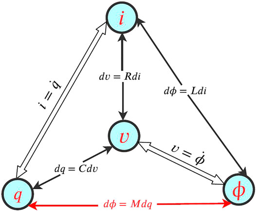
FIGURE 1. Symmetrical argument of the four basic passive circuit elements with respect to the four circuit variables.
For more than 3 decades, memristor remained a mystery until in 2008 (Strukov et al. (2008)) a group of researchers from the HP laboratory announced the successful realization of the first solid-state memristor in a device form (Stanley Williams (2013)). This recent discovery of the HP lab allured many scientists, engineers, and researchers to explore the feasible applications of memristor in discrete and crossbar array configurations Mazumder et al. (2012) and more possible device technologies.
Since the invention by Strukov et al. (2008), many memristor technologies emerged which are basically adhered to the principle of bipolar resistance switching between two extreme values, namely,
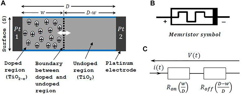
FIGURE 2. Structure of the TiO2 memristor. The doped region TiO2-e and the undoped region TiO2 are, respectively, the higher and lower conducting regions with resistance
The mathematical description of the titanium-oxide memristor when a positive voltage
where
where
A window function
Eq. 1 characterizes a bipolar memristor where the resistance switching depends on the voltage polarity (Strachan et al. (2011), Krzysteczko et al. (2009), Teixeira et al. (2009)). However, there are other reported memristors exhibiting symmetry in polarity, such as unipolar, nonpolar, and complementary resistive switching memristors (Yoshida et al. (2008), Huang et al. (2010), Wang et al. (2017), Linn et al. (2010)). Here, the resistance switching between
Many memristor-based applications are reported (Prodromakis and Toumazou (2010), Marani et al. (2015), including implementation of chaotic circuits and field programmable gate array (Muthuswamy (2010), Xu et al. (2016)), high-density memory and data storage (Duan et al. (2012), Hamdioui et al. (2015)), cellular neural networks (Thomas (2013), Duan et al. (2014)), neuromorphicmemristance for one system (Chu et al. (2014), Yakopcic et al. (2018)), and logic circuits (Borghetti et al. (2010), Shin et al. (2010)). A memristor is reported to be a promising element as synapse owing to its flexibility in conductance modulation and very effective high-density connectivity Jo et al. (2010), Adhikari et al. (2012), Kim et al. (2011). There are many implemented electronic memristor-based synapses for various neumorphic computing architectures (Lecerf et al. (2014), Li et al. (2014), Saïghi et al. (2015), Prezioso et al. (2016), Wang et al. (2016), Boyn et al. (2017), Dongale et al. (2018)).
The interesting features of memristors, such as connection flexibility, nanoscaleability, memory capability, and conductance modulation, are essential properties affirming the reliability of the memristor in neuromorphic networks, especially as synaptic function. The memristor is studied in the coupling mode between two neuron cells where the synchronization phenomena is investigated numerically and theoretically (Ascoli et al. (2015), Zhang and Liao (2017), Xu et al. (2018), Bao et al. (2020)). Unidirectional coupling and bidirectional or mutual coupling are the commonly used coupling modes for nonlinear chaotic systems (Volos et al. (2015)). The synchronization and chaos between two neuron cells is also investigated by using unidirectional and bidirectional coupling (Zhang and Liao (2017)).
The main application of our work is to use the memristor as a synaptic link between neurons in electronic models, as for example, in hybrid technologies with neuronal electronic prosthesis between real neurons. The network is initially composed of a linear capacitor and a nonlinear resistance in each cell and a linear resistor in series (Comte et al. (2001)), see Figure 3A. The equivalent memristor-based network is shown in Figure 3B where the series resistance is replaced by a memristor. The memory circuit element being intrinsically asymmetric (Di Ventra et al. (2009)), the TiO2 memristor crossbar is used to visualize the nature of current flowing through the device with respect to the polarities of the applied voltage. Using a memristor for the image processing technique was also reported by Prodromakis and Toumazou (2010), where a memristive grid is employed to perform edge detection. In a first step to implement 2D-memristor–based cellular nonlinear networks for signal and image processing purposes or for modeling a neural network with memristors as synapses, we rather focus here on the interaction of the memristor between pixel cells by considering a system of two cells in order to assess the behavior of the memristor quantitatively and qualitatively.
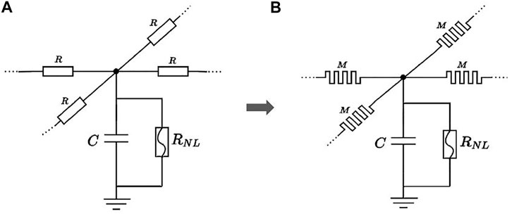
FIGURE 3. 2D cellular nonlinear networks (CNNs). C is a linear capacitor, and
The underlining task is accompanied by observing the pinched hysteresis loop (PHL), memristance transition, voltage evolution of the cells, and the explanation of the memristor’s lack of bilaterality. We derive analytically a second-order nonlinear differential equation characterizing the interaction of the memristor between the two cells bidirectionally. The system is studied in the phase plane allowing visualizing the memristor asymmetry. The memristance variation of a bipolar memristor with respect to the direction of flowing current affects its reliability in some potential applications where sensitivity in direction is important, for example, the memristive grid for neuromorphic application and image processing, hence the need for the so-called memristor fuse (Jiang and Shi (2009)). The formation is achieved by connecting two identical memristors antiserially. We describe the memristor fuse and obtain some results in accordance to our application.
2 Description of the Polarity Reversal
Figures 4A,B show two identical memristors
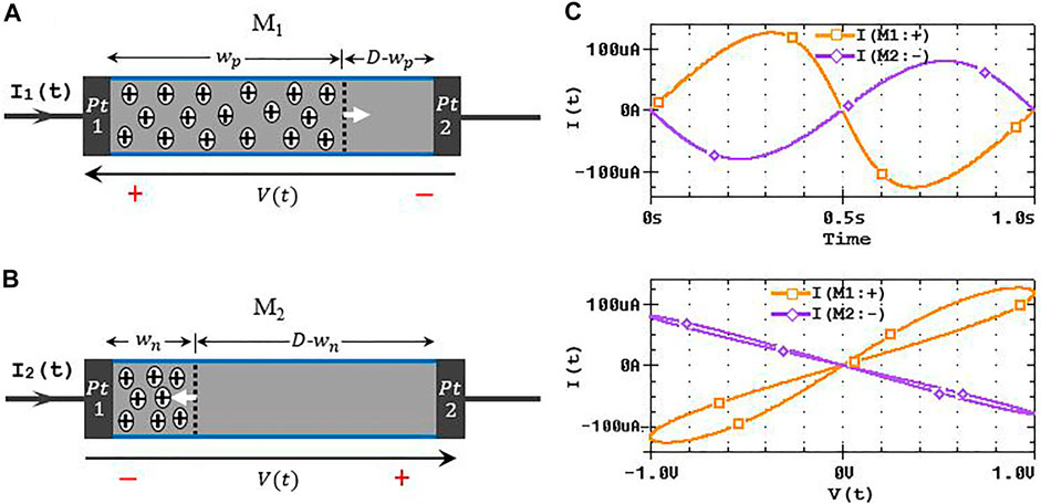
FIGURE 4. Concentration of the dopants in relation to charge carrier mobility with respect to the polarity of the input signal. (A) Application of positive bias causes the expansion of the doped region through the bulk of the device; (B) application of negative bias causes the contraction of the doped region (Joglekar and Wolf (2009)). Respectively, the overall process affects the device conducting channel widths
The schematic is shown in Figure 2A, where initially, the width of TiO2 altogether is D and the width of the doped (TiO2-e) region is w and the undoped one is
It follows that the conductivity of a memristor can be compared to that of a diode in terms of terminal polarity. However, unlike the diode, the memristor conducts electricity in both directions but the conductivity increases if its higher polarity terminal is connected to the positive terminal of the applied voltage source and decreases if its lower polarity terminal is connected to the positive terminal of the applied input voltage source.
In a nanoscale device, even small voltages can generate large electric field required to cause current to flow through the device. The smaller the device, the higher the electric field developed, and hence, more current flows through the device (Strukov et al. (2008)). The electroforming process forms the oxygen vacancies which cause a high-conducting channel (TiO2-e) shunting the bulk of the insulation film TiO2 (Yang et al. (2008), Pickett et al. (2009)). Depending on the nature of the bipolar input source, the conducting channel is affected by the variation of the tunneling barrier width (
3 Memristor Asymmetry From the Circuit Point of View
To vividly visualize the effect of memristor asymmetry, we consider two identical RC cells shown in Figure 5, which is the simplified setup of the system in the work of Isah et al. (2020b). The cells are labeled as cell-1 and cell-2 having potentials
1. Cond-1:
2. Cond-2:
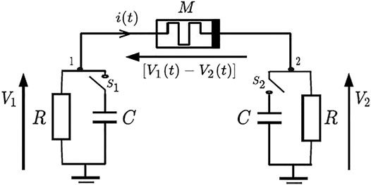
FIGURE 5. Memristor asymmetry from the circuit point of view: two charged RC cells coupled together by a memristor. The circuit is invoked by the switches
In the former, the direction of
where
Figure 5 is simulated in SPICE using the memristor model by Biolek et al. (2009), which can easily be implemented experimentally. The setup is activated by closing the switches
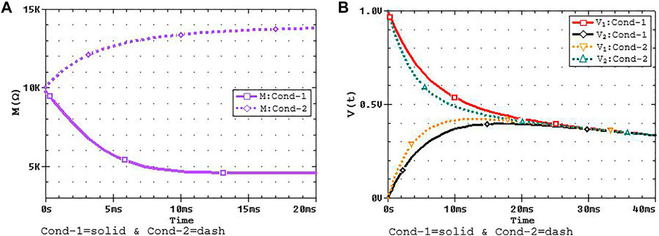
FIGURE 6. The interaction of the cells according to Cond-1 (solid curves) and Cond-2 (dash curves) for
In Cond-1, the memristance decreases corresponding to the expansion of the doped region; meanwhile, for Cond-2, the memristance increases corresponding to the contraction of the doped region. In both Cond-1 and Cond-2, the memristance transition eventually flattens as the cells stabilize, that is, at a time when
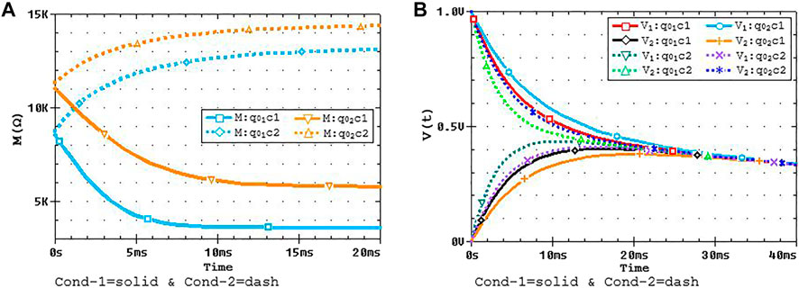
FIGURE 7. System evolution using two different initial charges
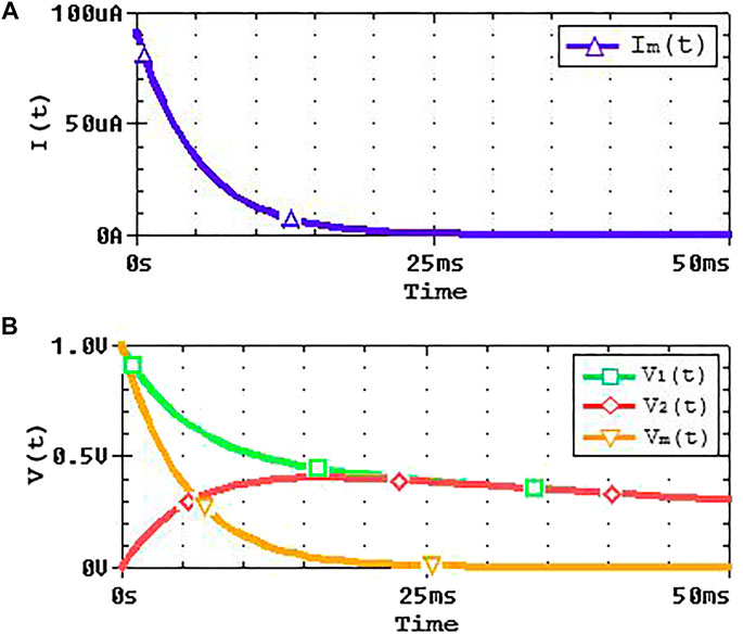
FIGURE 8. (A) Current through the memristor. (B) Evolution of
Furthermore, from Figure 5, one can deduce the following equations:
where
with
where
Eq. 12 can be expressed in a normalized form as
where
with
allowing to study the system in the phase plane (X,Y) which facilitates the observation of cell interaction in relation to the memristive effect under different initial conditions. Furthermore, Eq. 13 requires a continuous first derivative of
where H is a conservative expression for the equation set Eq. 15, only depending on the initial conditions
Recall that
and the analytical relation between the normalized time τ and the normalized charge X becomes
Here,
Furthermore, the equilibrium point of equation system Eq. 15 is met when
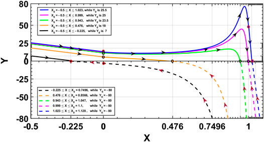
FIGURE 9. Phase portraits showing the charge evolution from left to right for
The phase portraits show the families of curves for different initial conditions. The results are obtained for
where
4 Memristor Fuse
The lack of bilaterality manifested in a bipolar memristor device is challenging in terms of its usage for certain applications, such as communication link in bidirectional applications (Comte et al. (2001)). As shown in Figure 6 and Figure 7, using a memristor to link two possible sources of information communicating together bidirectionally is not advisable owing to its resistance dependency on the amount and direction of flowing current. To convert it, a memristor fuse is proposed and then demonstrated in the work of Jiang and Shi (2009), Gelencser et al. (2012), and Serb et al. (2016). It is basically formed by connecting two memristors antiserially in order to avoid the lack of bilaterality (Yildirim et al. (2018)). The memristor fuse is reported to be useful in a memristive grid network for CNN neighborhood connection and image processing (Pershin and Di Ventra (2011), Gelencser et al. (2012), Yang and Kim (2016), Yildirim et al. (2018), Sarmiento-Reyes and Rodríguez-Velásquez (2018), Lim et al. (2019)). In general (Fouda et al. (2013)), Figure 10 shows the four possible ways to form series connections of two memristors with respect to their polarities.
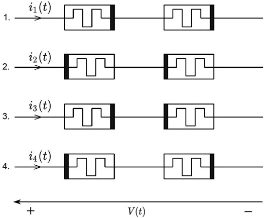
FIGURE 10. Four possible series connections of two memristors with respect to the input source. The memristive effect is retained for cases 1 and 2 whereas it is balanced for cases 3 and 4 (Joglekar and Wolf (2009)). Although cases 3 and 4 are identical and both form a memristor fuse, only case 3 is commonly considered as memristor fuse formation (Gelencser et al. (2012)).
As shown in Figure 10, cases 1 and 2 refer to a serial connection of two memristors and the memristive effect is retained for these branches. Meanwhile, cases 3 and 4 are identical in structure and refer to antiserial connection of two memristors, thus forming a memristor fuse. The memristive effect for branches in cases 3 and 4 could be suppressed (Joglekar and Wolf (2009)). However, case 3 is the commonly adopted formation of a memristor fuse (Gelencser et al. (2012)). Note that cases 1 and 2 resemble Figures 4A,B, respectively, with the exception that two memristors are involved.
It is important to note that the resistance of the memristor fuse is the sum of the resistance of each of the individual memristor because the equivalent memristance is additive in a serially connected memristor. In addition, this could be a disadvantage to the desired amount of current and it also affects the dynamic features of the memristor to the extent that the current–voltage graph is merely linear; hence, the formation resembles normal resistor. Therefore, the resistance limits of the memristor fuse must be the same as those of memristor if acting alone.
The pinched hysteresis loop is one of the most distinguished fingerprints of a memristor (Adhikari et al. (2013), Chua (2014)) and is a reflection of its memory effect. As pointed out in the work of Chua (1971) and Chua (2015), without the memory, a memristor is nothing different from a resistor. A verification test is performed to compare the memristor fuse with a standalone memristor, as demonstrated in Figure 11.
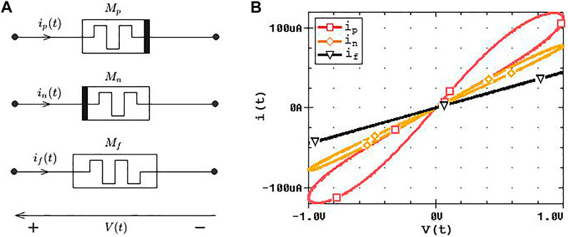
FIGURE 11. Circuit response comparison of a memristor fuse with standalone memristors. (A) Circuit schematic with a sine input voltage source.
Figure 12 shows the schematic of a memristor fuse formed by antiseries connection of two memristors
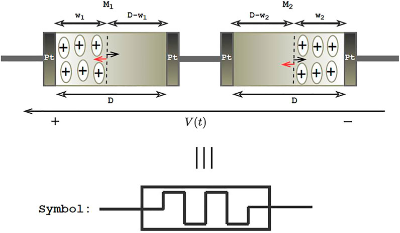
FIGURE 12. Schematic of a memristor fuse formed by two TiO2 memristors
The same current flows through a series connection of two memristors; hence,
where
where
where
The instantaneous memristance of the memristor fuse depends then on the mismatch factor (ϱ).
Figure 13 shows the comparison of the circuit response for the memristor and memristor fuse using the setup shown in Figure 5. Then, for Cond-1,
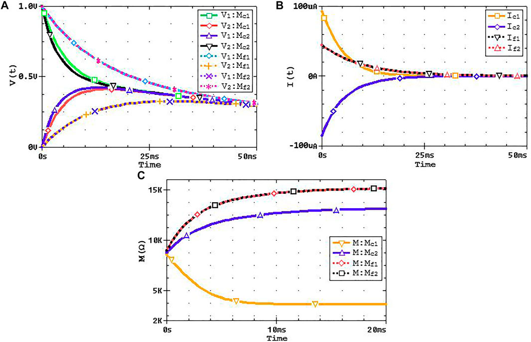
FIGURE 13. Comparing the system evolution using the circuit of Figure 5 by considering memristor (M) and then memristor fuse (Mf). Mc1 and Mc2 correspond, respectively, to a single memristor used according to Cond-1 and Cond-2, while Mf1 and Mf2 correspond, respectively, to a memristor fuse used according to Cond-1 and Cond-2. The results show the response for each case until the system stabilized: (A) the voltage evolution as
Figure 13A shows the evolution of
5 Conclusion
We introduced the application of memristor in a nonlinear network, focusing specifically on the behavior of the memristor with respect to the polarity reversal effect of the input signal. Our target is the implementation of memristor-based 2D nonlinear networks for versatile applications, such as signal processing and electronic prosthesis for a synaptic link between real neurons. Here, we investigate the interaction of a bipolar memristor between two RC cells communicating together bidirectionally. In this way, the interaction of the memristor within the network is studied qualitatively and quantitatively. We have shown from the circuit point of view and the analytical solution that the conductivity of the memristor depends on the polarity of the applied input signal, thus affecting the mobility of its charge carriers, this property being due to the intrinsic nature of the device. It is an inevitable nature of a bipolar memristor, irrespective of its device technology. Hence, the memristive effect changes according to the connection mode and the amount of current flowing through it, showing that the memristor is not a bilateral circuit element as verified by our study.
To achieve the memristive effect with symmetry, a memristor fuse is proposed. We present the detail analytical interpretation of the memristor fuse. We also authenticate the memristor fuse prior to apply it in a circuit, and the results show that the memristor fuse behaves like a standalone memristor under high input frequency. Although connecting two memristors antiserially to form a memristor fuse lets the dynamic of the two state variables system become more intricate, as well as the dynamics of the resistance switching (Serb et al. (2016)), terminals’ asymmetry is resolved as confirmed by the results shown in Figure 13. The symmetry displayed by the memristor fuse suggests it to be a promising element useful as a memristive grid in neighborhood connections and it could become an important concept for the ongoing study of our memristor-based network.
Data Availability Statement
The original contributions presented in the study are included in the article/Supplementary Material; further inquiries can be directed to the corresponding authors.
Author Contributions
All authors listed have made a substantial, direct, and intellectual contribution to the work and approved it for publication.
Conflict of Interest
The authors declare that the research was conducted in the absence of any commercial or financial relationships that could be construed as a potential conflict of interest.
References
Adhikari, S. P., Changju Yang, C., Hyongsuk Kim, H., and Chua, L. O. (2012). Memristor Bridge Synapse-Based Neural Network and its Learning. IEEE Trans. Neural Netw. Learn. Syst. 23, 1426–1435. doi:10.1109/tnnls.2012.2204770
Adhikari, S. P., Sah, M. P., Kim, H., and Chua, L. O. (2013). Three Fingerprints of Memristor. IEEE Trans. Circuits Syst. 60, 3008–3021. doi:10.1109/tcsi.2013.2256171
Ascoli, A., Lanza, V., Corinto, F., and Tetzlaff, R. (2015). Synchronization Conditions in Simple Memristor Neural Networks. J. Franklin Inst. 352, 3196–3220. doi:10.1016/j.jfranklin.2015.06.003
Bao, B., Yang, Q., Zhu, D., Zhang, Y., Xu, Q., and Chen, M. (2020). Initial-induced Coexisting and Synchronous Firing Activities in Memristor Synapse-Coupled Morris-Lecar Bi-neuron Network. Nonlinear Dyn. 99, 2339–2354. doi:10.1007/s11071-019-05395-7
Biolek, Z., Biolek, D., and Biolková, V. (2012). Computation of the Area of Memristor Pinched Hysteresis Loop. IEEE Trans. Circuits Syst. 59, 607–611. doi:10.1109/tcsii.2012.2208670
Biolek, Z., Biolek, D., and Biolkova, V. (2009). Spice Model of Memristor with Nonlinear Dopant Drift. Radioengineering 18 (2), 210–214.
Borghetti, J., Snider, G. S., Kuekes, P. J., Yang, J. J., Stewart, D. R., and Williams, R. S. (2010). 'Memristive' Switches Enable 'stateful' Logic Operations via Material Implication. Nature 464, 873–876. doi:10.1038/nature08940
Boyn, S., Grollier, J., Lecerf, G., Xu, B., Locatelli, N., Fusil, S., et al. (2017). Learning through Ferroelectric Domain Dynamics in Solid-State Synapses. Nat. Commun. 8, 14736–14737. doi:10.1038/ncomms14736
Campbell, K. A. (2017). Self-directed Channel Memristor for High Temperature Operation. Microelectronics J. 59, 10–14. doi:10.1016/j.mejo.2016.11.006
Chu, M., Kim, B., Park, S., Hwang, H., Jeon, M., Lee, B. H., et al. (2014). Neuromorphic Hardware System for Visual Pattern Recognition with Memristor Array and Cmos Neuron. IEEE Trans. Ind. Electro. 62, 2410–2419. doi:10.1109/tie.2014.2356439
Chua, L. (2015). Everything You Wish to Know about Memristors but Are Afraid to Ask. Radioengineering 24, 319–368. doi:10.13164/re.2015.0319
Chua, L. (2014). If It's Pinched It's a Memristor. Semicond. Sci. Technol. 29, 104001. doi:10.1088/0268-1242/29/10/104001
Chua, L. (1971). Memristor-the Missing Circuit Element. IEEE Trans. Circuit Theor. 18, 507–519. doi:10.1109/tct.1971.1083337
Chua, L. O., and Sung Mo Kang, S. M. (1976). Memristive Devices and Systems. Proc. IEEE 64, 209–223. doi:10.1109/proc.1976.10092
Comte, J. C., Marquié, P., and Bilbault, J. M. (2001). Contour Detection Based on Nonlinear Discrete Diffusion in a Cellular Nonlinear Network. Int. J. Bifurcation Chaos 11, 179–183. doi:10.1142/s0218127401002134
Di Ventra, M., Pershin, Y. V., and Chua, L. O. (2009). Putting Memory into Circuit Elements: Memristors, Memcapacitors, and Meminductors [point of View]. Proc. IEEE 97, 1371–1372. doi:10.1109/jproc.2009.2022882
Dongale, T. D., Desai, N. D., Khot, K. V., Volos, C. K., Bhosale, P. N., and Kamat, R. K. (2018). An Electronic Synapse Device Based on Tio2 Thin Film Memristor. J. Nanoelectronics Optoelectronics 13, 68–75. doi:10.1166/jno.2018.2297
Duan, S., Hu, X., Dong, Z., Wang, L., and Mazumder, P. (2015). Memristor-based Cellular Nonlinear/neural Network: Design, Analysis, and Applications. IEEE Trans. Neural Netw. Learn. Syst. 26, 1202–1213. doi:10.1109/TNNLS.2014.2334701
Duan, S., Hu, X., Wang, L., Li, C., and Mazumder, P. (2012). Memristor-based Rram with Applications. Sci. China Inf. Sci. 55, 1446–1460. doi:10.1007/s11432-012-4572-0
Fouda, M. E., Khatib, M. A., Mosad, A. G., and Radwan, A. G. (2013). Generalized Analysis of Symmetric and Asymmetric Memristive Two-Gate Relaxation Oscillators. IEEE Trans. Circuits Syst. 60, 2701–2708. doi:10.1109/tcsi.2013.2249172
Gelencser, A., Prodromakis, T., Toumazou, C., and Roska, T. (2012). A Biomimetic Model of the Outer Plexiform Layer by Incorporating Memristive Devices. Phys. Rev. E 85, 041918. doi:10.1103/physreve.85.041918
Hamdioui, S., Xie, L., Du Nguyen, H. A., Taouil, M., Bertels, K., Corporaal, H., et al. (2015). Memristor Based Computation-In-Memory Architecture for Data-Intensive Applications, 2015 Design, Automation & Test in Europe Conference & Exhibition (DATE); March 2015; Grenoble, France. IEEE, 1718–1725.
Huang, H.-H., Shih, W.-C., and Lai, C.-H. (2010). Nonpolar Resistive Switching in the Pt/mgo/pt Nonvolatile Memory Device. Appl. Phys. Lett. 96, 193505. doi:10.1063/1.3429024
Isah, A., Nguetcho, A. S. T., Binczak, S., and Bilbault, J. M. (2020a). Memristor Dynamics Involved in Cells Communication for a 2D Non‐linear Network. IET Signal. Process. 14, 427–434. doi:10.1049/iet-spr.2020.0136
Isah, A., Nguetcho, A. T., Binczak, S., and Bilbault, J. (2020b). Dynamics of a Charge-Controlled Memristor in Master–Slave Coupling. Electro. Lett. 56, 168. doi:10.1049/el.2019.3322
Jiang, F., and Shi, B. E. (2009). The Memristive Grid Outperforms the Resistive Grid for Edge Preserving Smoothing, 2009 European Conference on Circuit Theory and Design (IEEE); Aug. 2009; Antalya, Turkey. doi:10.1109/ECCTD.2009.5274947IEEE, 181–184.
Jo, S. H., Chang, T., Ebong, I., Bhadviya, B. B., Mazumder, P., and Lu, W. (2010). Nanoscale Memristor Device as Synapse in Neuromorphic Systems. Nano Lett. 10, 1297–1301. doi:10.1021/nl904092h
Joglekar, Y. N., and Wolf, S. J. (2009). The Elusive Memristor: Properties of Basic Electrical Circuits. Eur. J. Phys. 30, 661–675. doi:10.1088/0143-0807/30/4/001
Kim, H., Sah, M. P., Yang, C., Roska, T., and Chua, L. O. (2011). Memristor Bridge Synapses, Proceedings of the IEEE, 100. IEEE, 2061–2070. doi:10.1109/JPROC.2011.2166749
Krzysteczko, P., Reiss, G., and Thomas, A. (2009). Memristive Switching of Mgo Based Magnetic Tunnel Junctions. Appl. Phys. Lett. 95, 112508. doi:10.1063/1.3224193
Lecerf, G., Tomas, J., Boyn, S., Girod, S., Mangalore, A., Grollier, J., et al. (2014). Silicon Neuron Dedicated to Memristive Spiking Neural Networks, 2014 IEEE International Symposium on Circuits and Systems (ISCAS); June 2014; Melbourne, VIC, Australia. doi:10.1109/ISCAS.2014.6865448IEEE, 1568–1571.
Li, Y., Zhong, Y., Zhang, J., Xu, L., Wang, Q., Sun, H., et al. (2014). Activity-dependent Synaptic Plasticity of a Chalcogenide Electronic Synapse for Neuromorphic Systems. Sci. Rep. 4, 4906. doi:10.1038/srep04906
Lim, C. K. K., Gelencser, A., and Prodromakis, T. (2019). Computing Image and Motion with 3-d Memristive Grids. Handbook of Memristor. Networks (Springer), 1177–1210.
Linn, E., Rosezin, R., Kügeler, C., and Waser, R. (2010). Complementary Resistive Switches for Passive Nanocrossbar Memories. Nat. Mater 9, 403–406. doi:10.1038/nmat2748
Marani, R., Gelao, G., and Perri, A. G. (2015). A Review on Memristor Applications. arXiv preprint arXiv:1506.06899
Mazumder, P., Kang, S. M., and Waser, R. (2012). Memristors: Devices, Models, and Applications [Scanning the Issue]. Proc. IEEE 100, 1911–1919. doi:10.1109/jproc.2012.2190812
Muthuswamy, B. (2010). Implementing Memristor Based Chaotic Circuits. Int. J. Bifurcation Chaos 20, 1335–1350. doi:10.1142/s0218127410026514
Paris, A., and Taioli, S. (2016). Multiscale Investigation of Oxygen Vacancies in TiO2 Anatase and Their Role in Memristor's Behavior. J. Phys. Chem. C 120, 22045–22053. doi:10.1021/acs.jpcc.6b07196
Pershin, Y. V., and Di Ventra, M. (2011). Solving Mazes with Memristors: A Massively Parallel Approach. Phys. Rev. E 84, 046703. doi:10.1103/physreve.84.046703
Pickett, M. D., Strukov, D. B., Borghetti, J. L., Yang, J. J., Snider, G. S., Stewart, D. R., et al. (2009). Switching Dynamics in Titanium Dioxide Memristive Devices. J. Appl. Phys. 106, 074508. doi:10.1063/1.3236506
Prezioso, M., Bayat, F. M., Hoskins, B., Likharev, K., and Strukov, D. (2016). Self-adaptive Spike-time-dependent Plasticity of Metal-Oxide Memristors. Scientific Rep. 6, 1–6. doi:10.1038/srep21331
Prodromakis, T., and Toumazou, C. (2010). A Review on Memristive Devices and Applications, 2010 17th IEEE International Conference on Electronics, Circuits and Systems; Dec. 2010; Athens, Greece. IEEE, 934–937. doi:10.1109/ICECS.2010.5724666
Saïghi, S., Mayr, C. G., Serrano-Gotarredona, T., Schmidt, H., Lecerf, G., Tomas, J., et al. (2015). Plasticity in Memristive Devices for Spiking Neural Networks. Front. Neurosci. 9, 51. doi:10.3389/fnins.2015.00051
Sarmiento-Reyes, A., and Rodríguez-Velásquez, Y. (2018). Maze-solving with a Memristive Grid of Charge-Controlled Memristors (LASCAS), 2018 IEEE 9th Latin American Symposium on Circuits & Systems; Feb. 2018; Puerto Vallarta, Mexico. (IEEE), 1–4. doi:10.1109/LASCAS.2018.8399973
Serb, A., Khiat, A., and Prodromakis, T. (2016). Practical Demonstration of a Memristive Fuse. arXiv preprint arXiv:1609.02410
Shin, S., Kim, K., and Kang, S.-M. (2010). Memristor Applications for Programmable Analog IcsIEEE Transactions on Nanotechnology, 10. (IEEE), 266–274. doi:10.1109/TNANO.2009.2038610
Simmons, J. G. (1971). Conduction in Thin Dielectric Films. J. Phys. D: Appl. Phys. 4, 613–657. doi:10.1088/0022-3727/4/5/202
Simmons, J. G. (1963a). Electric Tunnel Effect between Dissimilar Electrodes Separated by a Thin Insulating Film. J. Appl. Phys. 34, 2581–2590. doi:10.1063/1.1729774
Simmons, J. G. (1963b). Generalized Formula for the Electric Tunnel Effect between Similar Electrodes Separated by a Thin Insulating Film. J. Appl. Phys. 34, 1793–1803. doi:10.1063/1.1702682
Stanley Williams, R. (2013). How We Found the Missing Memristor, Chaos, CNN, Memristors and Beyond: A Festschrift for Leon Chua With DVD-ROM, composed by Eleonora Bilotta (World Scientific). (IEEE), 483–489. doi:10.1109/MSPEC.2008.4687366
Strachan, J. P., Strukov, D. B., Borghetti, J., Joshua Yang, J., Medeiros-Ribeiro, G., and Stanley Williams, R. (2011). The Switching Location of a Bipolar Memristor: Chemical, thermal and Structural Mapping. Nanotechnology 22, 254015. doi:10.1088/0957-4484/22/25/254015
Strukov, D. B., Snider, G. S., Stewart, D. R., and Williams, R. S. (2008). The Missing Memristor Found. nature 453, 80–83. doi:10.1038/nature06932
Teixeira, J. M., Ventura, J., Fermento, R., Araujo, J. P., Sousa, J. B., Wisniowski, P., et al. (2009). Electroforming, Magnetic and Resistive Switching in Mgo-Based Tunnel Junctions. J. Phys. D: Appl. Phys. 42, 105407. doi:10.1088/0022-3727/42/10/105407
Thomas, A. (2013). Memristor-based Neural Networks. J. Phys. D: Appl. Phys. 46, 093001. doi:10.1088/0022-3727/46/9/093001
Volos, C. K., Kyprianidis, I., Stouboulos, I., Tlelo-Cuautle, E., and Vaidyanathan, S. (2015). Memristor: A New Concept in Synchronization of Coupled Neuromorphic Circuits. J. Eng. Sci. Techn. Rev. 8. doi:10.25103/jestr.082.21
Wang, C., He, W., Tong, Y., and Zhao, R. (2016). Investigation and Manipulation of Different Analog Behaviors of Memristor as Electronic Synapse for Neuromorphic Applications. Sci. Rep. 6, 22970. doi:10.1038/srep22970
Wang, Z., Joshi, S., Savel’ev, S. E., Jiang, H., Midya, R., Lin, P., et al. (2017). Memristors with Diffusive Dynamics as Synaptic Emulators for Neuromorphic Computing. Nat. Mater 16, 101–108. doi:10.1038/nmat4756
Xu, F., Zhang, J., Fang, T., Huang, S., and Wang, M. (2018). Synchronous Dynamics in Neural System Coupled with Memristive Synapse. Nonlinear Dyn. 92, 1395–1402. doi:10.1007/s11071-018-4134-0
Xu Ya-Ming, Y.-M., Wang Li-Dan, L.-D., and Duan Shu-Kai, S.-K. (2016). A Memristor-Based Chaotic System and its Field Programmable Gate Array Implementation. wlxb 65, 120503. doi:10.7498/aps.65.120503
Yakopcic, C., Hasan, R., and Taha, T. M. (2018). Flexible Memristor Based Neuromorphic System for Implementing Multi-Layer Neural Network Algorithms. Int. J. Parallel, Emergent Distributed Syst. 33, 408–429. doi:10.1080/17445760.2017.1321761
Yang, C., and Kim, H. (2016). Linearized Programming of Memristors for Artificial Neuro-Sensor Signal Processing. Sensors 16, 1320. doi:10.3390/s16081320
Yang, J. J., Pickett, M. D., Li, X., Ohlberg, D. A. A., Stewart, D. R., and Williams, R. S. (2008). Memristive Switching Mechanism for Metal/oxide/metal Nanodevices. Nat. Nanotech 3, 429–433. doi:10.1038/nnano.2008.160
Yildirim, M., Babacan, Y., and Kacar, F. (2018). Memristive Retinomorphic Grid Architecture Removing Noise and Preserving Edge. AEU - Int. J. Electro. Commun. 97, 38–44. doi:10.1016/j.aeue.2018.10.001
Yin, L., Cheng, R., Wang, Z., Wang, F., Sendeku, M. G., Wen, Y., et al. (2020). Two-dimensional Unipolar Memristors with Logic and Memory Functions. Nano Lett. 20, 4144–4152. doi:10.1021/acs.nanolett.0c00002
Yoshida, C., Kurasawa, M., Lee, Y. M., Aoki, M., and Sugiyama, Y. (2008). Unipolar Resistive Switching in CoFeB∕MgO∕CoFeB Magnetic Tunnel junction. Appl. Phys. Lett. 92, 113508. doi:10.1063/1.2898514
Keywords: cellular nonlinear networks, memristor, bilateral, asymmetry, charged cells, memristor fuse
Citation: Isah A, Tchakoutio Nguetcho AS, Binczak S and Bilbault J (2021) Polarity Reversal Effect of a Memristor From the Circuit Point of View and Insights Into the Memristor Fuse. Front. Comms. Net 2:647528. doi: 10.3389/frcmn.2021.647528
Received: 06 January 2021; Accepted: 15 June 2021;
Published: 07 July 2021.
Edited by:
Ilangko Balasingham, Norwegian University of Science and Technology, NorwayReviewed by:
Valentina Lanza, University of Le Havre, FranceZhongrui Wang, The University of Hong Kong, China
Copyright © 2021 Isah, Tchakoutio Nguetcho, Binczak and Bilbault. This is an open-access article distributed under the terms of the Creative Commons Attribution License (CC BY). The use, distribution or reproduction in other forums is permitted, provided the original author(s) and the copyright owner(s) are credited and that the original publication in this journal is cited, in accordance with accepted academic practice. No use, distribution or reproduction is permitted which does not comply with these terms.
*Correspondence: Aliyu Isah, YWxpeXVfaXNhaEBldHUudS1ib3VyZ29nbmUuZnI=, YWxpeXVpc2FoYmFiYW50YUBnbWFpbC5jb20=; J.M. Bilbault, amVhbi1tYXJpZS5iaWxiYXVsdEB1LWJvdXJnb2duZS5mcg==.