Abstract
Fully depleted CMOS sensors represent a significant step forward in radiation detection, combining the advantages of monolithic active pixel sensors with the enhanced signal collection efficiency of depleted bulk materials. The ARCADIA Collaboration established a technology platform for the development and production of deep sub-micron fully depleted CMOS monolithic sensors with excellent collection efficiency, advancing this semiconductor detector technology with IP cores, ASICs, and back-end dedicated acquisition systems. The sensor technology was demonstrated on system-ready full chip monolithic active pixel sensors with high rate capability and very low power for the detection of charged particles and photons. Innovative CMOS monolithic LGADs featuring a shallow gain layer and implementing a low-gain avalanche diode were developed for time-of-flight detectors, while other prototype ASICs have implemented multi-threshold photon-counting architectures for X-ray imaging. The implementation of fully depleted monolithic strip sensors with embedded electronics and low power density makes the proposed approach a good candidate for future detectors in space applications. The ARCADIA technology will find applications in medical instruments, nuclear imaging and dosimetry, frontier detectors for experimental high energy, and astroparticle physics. This review details the main development achievements by describing the technology demonstrators fabricated and tested and provides a detailed overview of the characteristics and architecture of the ARCADIA-MD3 full-chip monolithic active pixel sensor.
1 Monolithic CMOS pixel detectors
Monolithic complementary metal-oxide semiconductor (CMOS) sensors integrate sensor, readout, and processing electronics in the same silicon substrate. These are fabricated in microelectronics silicon foundries typically focused on CMOS Image Sensor (CIS) technology, with a manufacturing capability in the range of several thousand wafers per week. In the framework of the development of radiation detectors for particle and nuclear physics, CMOS sensors are a very competitive solution compared to traditional hybrid pixel or micro-strip detectors, allowing for significant potential gains in terms of performance, increased robustness, and lower production costs.
In early proposed solutions for the use of a CMOS technology for tracking detectors in high-energy physics (Hillemanns et al., 2013), the signal is collected on a relatively shallow epitaxial layer (typically 15–30 ). The charge carriers generated from the incident particle or photon are transported through diffusion and collected by a small collection electrode. The resulting signal is processed with on-pixel CMOS front-end electronics, which includes both analog and digital circuitry. A significant milestone in this field was achieved with the production of the sensors used to instrument the inner tracker ITS2 of the ALICE experiment at CERN during the detector upgrade in 2021 (Ravasenga, 2024). However, the long collection time intrinsic to the diffusion process makes these sensors unfit for operation under high fluxes of neutrons or charged particles causing bulk damage or generally in applications where high time resolution is required. In addition, the limited thickness of these devices does not allow for soft X-ray imaging with sufficient efficiency. Modifications of this process were subsequently proposed with an additional implant introduced to allow the full depletion of the 25 epitaxial layer (Pernegger et al., 2017), while the migration from a TJ 180 nm to a TPSCo 65 nm technology node is now paving the way for future upgrades of the ALICE inner tracker (Ferrero, 2024).
Other approaches embed the electronics in a large collecting electrode, which can be implemented either with a deep nwell or a buried layer, both structures having become standard in modern deep sub-micron processes. The large collection electrode guarantees a uniform electric field across the sensor, allowing for better radiation hardness up to fluences of . The common implementation of such HV-CMOS sensors uses a p-sub contact on the top side, and the readout circuitry is built inside a deep n-well which isolates the CMOS electronics from the sensor high-voltage bias (Perić et al., 2021). Notwithstanding, this approach has two major drawbacks: the large collecting electrode creates a large parasitic capacitance, while the electronics embedded inside the sensor introduce positive feedback between the preamplifier-discriminator and the sensor itself. A higher bias current is thus necessary, and current-mode logic can be indispensable for avoiding the coupling issues; both lead to a generally higher power dissipation than small collection electrode sensor technology.
An interesting alternative, based on silicon-on-insulator wafers, most commonly uses a buried oxide that separates a thick, high-resistivity sensor layer from a thin, microelectronics-grade layer to create the substrate for the CMOS electronics (Arai et al., 2017). The thickness of the sensing layer can be chosen in a wide range, thus allowing its optimization for the applications of interest. However, the use of SOI wafers entails two critical issues. On the one hand, the high voltage required to deplete the sensors couples through the buried oxide to the thin CMOS substrate, causing a shift of the threshold voltage of the MOSFETs. This problem was addressed by introducing a buried p-well that shields the CMOS layer from the high voltage, although the shape of such a p-well must be carefully optimized to avoid performance degradation due to the increase of the sensor capacitance. On the other hand, SOI-based sensors are prone to accumulate charge in the buried oxide layer after irradiation, which can degrade the performance of the CMOS circuitry. This is typically solved by using a second buried oxide layer for which the inner silicon layer, encapsulated between the two oxides and biased with a dedicated voltage domain, counteracts the effect of the accumulated charge. This layered implementation significantly increases the cost of the substrate procurement and wafer processing of this highly specialized technology.
Fully depleted CMOS sensors, featuring a completely depleted substrate with a thickness of several hundred micrometers, with the charge collected exclusively by drift, offer the possibility of replacing conventional hybrid pixels and strips in most applications. This possibility is hence relevant for experiments employing silicon detectors on future particle colliders and astroparticle physics experiments in space, with a potential application also in the medical field. The technology proposed in this study allows for the implementation of silicon sensors with an active thickness of up to 500 using a reduced set of custom process masks for fabrication in the standard LF11IS CMOS process at LFoundry.
2 The ARCADIA CMOS sensor technology
The SEED and ARCADIA projects, funded by the INFN CSN5, established a collaboration with the silicon foundry LFoundry s.r.l. to create an INFN platform to develop and produce high-efficiency deep-submicron CMOS monolithic sensors. These are implemented on n-type high-resistivity wafers with a typical final thickness ranging from to . The top side of the wafer is processed with LFoundry’s CMOS 110 nm node technology featuring six metal layers and 1.2 V NMOS/PMOS devices isolated with a deep p-well, while the back of the wafer features a p-n junction realized with a p+ implantation. The process uses an epitaxial layer where the increased doping concentration allows control of the potential beneath the deep p-well, moving the punch-through between the backside p+ electrode and the top p-type regions toward higher voltage values. The n-epi layer was engineered in such a way that the collection electrode can be biased at a voltage below 1 V, enabling the use of thin oxide 1.2 V core devices for better radiation tolerance. A detailed insight on the sensor technology and performance can be found in Pancheri et al. (2020).
Figure 1A illustrates the cross-section of a pixel array chip with a backside bias electrode on a heavily doped bias layer, forming the backside junction. The depletion layer hence develops from the backside of the n-type substrate when a negative bias voltage is applied to the p+ electrode. The choice of using the backside junction to bias the sensor allows for a full depletion of the substrate without the need to apply high voltage potentials at the front side, thus enabling the use of low-voltage CMOS electronics to read out the fast signals produced by electron drift current. The backside is processed after thinning to the final thickness and implanting a very shallow p+ boron-doped region subsequently activated with a laser annealing; Figure 1B illustrates a sensor thinned down to 200 before backside lithography. The possibility of post-processing the backside with lithography allows the creation of a multiple floating guard-ring termination structure around the sensor active area, avoiding early edge breakdown at the borders of the p+/n+ substrate junction. For tracking applications requiring thinner sensors ( or below), the sensor can be implemented without the need for the lithography processing of the backside, thus avoiding the use of the backside floating guard rings (Figure 1C). Alternatively, very thin sensors can be fabricated, starting from a p+ substrate with the double epitaxial layer grown on top (Figure 1D).
FIGURE 1

Detailed cross-section of the ARCADIA fully depleted CMOS sensor technology, depicting the arrangement of the pixel array and guard-ring terminations on the back-side (A). Embodiments of the technology for thicker sensors with backside lithography (B), for thinner sensors with maskless backside using a p+ implantation (C), and a maskless option (C) using a p+ starting substrate as a passive carrier (D).
3 ARCADIA prototypes and full-chip demonstrators
Involving seven INFN divisions and over 50 researchers and engineers, the ARCADIA1 initiative advanced semiconductor sensor technology while also developing IP cores, ASICs, and dedicated data acquisition systems. This collaboration demonstrated the scalability and technology readiness of the proposed MAPS sensor through the development of a full-size system-ready demonstrator featuring a low-power, high-density pixel matrix CMOS monolithic sensor. Other deliverables of the project include passive pixel and strip test structures for sensor characterization, monolithic silicon strip arrays with embedded readout electronics and silicon strip readout ASICs, test vehicles for multi-threshold photon counting architectures, small-scale prototypes for ultra-low power and fast timing, and mixed-signal ASICs for fast timing with sensors implementing a gain layer. The circuits and sensors were produced through a series of single-project wafer engineering runs employing different splits of starting substrate, process options, and final wafer thicknesses. The list of designs on board the ARCADIA engineering runs and its correspondence to the reticle floorplan (Figure 2) is depicted below.
FIGURE 2
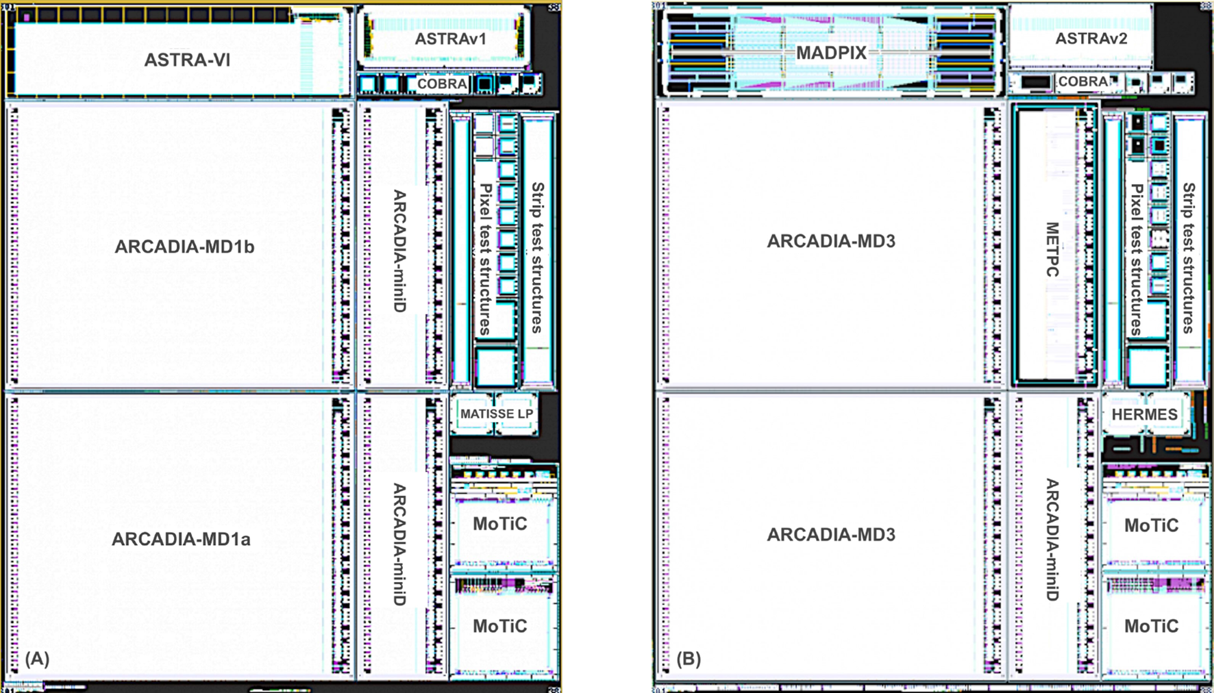
Reticle floorplans for the ARCADIA engineering runs, mask sets for the first (A) and second (B) single-project wafer productions.
3.1 ARCADIA-MD3 FD-MAPS main demonstrator (512 × 512 pixels)
The system-ready fully depleted monolithic active pixel sensor has an active area of 1.6 on a matrix with 262 K pixels featuring a pitch of 25 . The data-driven binary readout allows for a rate capability of 100 MHz/cm2; with a total power density of 17-30 mW/cm2; for low-rate operation, the power density is below 10 mW/cm2. The first engineering run included two full-chip designs with different front-end circuit topologies labelled as MD1a and MD1b, thoroughly characterized after a focused ion-beam correction of a connectivity issue at the level of the data transceiver control. The ARCADIA-MD3 design implements the needed corrective actions and was sent for fabrication on a second single-project wafer production. The readout logic, floorplan, and chip organisation of the ARCADIA-MD3 chip are detailed here in Section 4.
3.2 ARCADIA-miniD FD-MAPS mini demonstrator (512 × 32 pixels)
Smaller FD-MAPS demonstrators for testability and debugging implemented power management IPs (Bianco, 2021; Traversi et al., 2023) and configurability options for yield optimization on large sensors, using a dedicated low drop-out LDO regulator for each section of the chip.
3.3 FD-MAPS and test structures for timing applications
Third-party designs from the Paul Scherrer Institute PSI and ETH Zurich for timing applications. Details on the design characteristics and silicon results of MoTiC (Monolithic Pixel Detector with Timing) can be found in Burkhalter et al. (2024).
3.4 MATISSE low power front-end
MATISSE-LP is a small-scale FD-MAPS prototype featuring a 2 × 2 matrix with pixels and an ultra low-power front-end. The matrix is organized into four sectors of six columns each, each column embedding 24 pixels with a 50 pitch. The compact discrete-time pixel amplifier is based on a source follower input stage which is AC coupled to the discriminator with offset compensation, the pseudo-CMOS binary output being then propagated to the chip periphery. The estimated power density, based on post-layout simulations and with 11.2 nW/pixel at a rolling-shutter readout frequency of 10 kHz, is expected to be below 0.5 mW/cm2 (Durando, 2021).
3.5 Passive pixel and strip test structures
Arrays of passive pixels with parallel connections used for electrical characterisation (I-V and C-V curves with probe station) were used, with studies of charge collection efficiency and tests with pulsed IR and NIR lasers. Both pixel and matrix test structures implement pitches ranging from 50 down to 10 , with and without a gain layer (Neubüser et al., 2021; De Cilladi et al., 2021; Ferrero et al., 2023; Corradino et al., 2024).
3.6 ASTRA 64-channel mixed signal ASIC for Si-Strip readout
A mixed-signal silicon strip readout ASIC for space-borne experiments with very low-power performance (mW/channel) and low-noise (ENC below 1,000 ) used a bi-polar input stage optimized for sensor capacitance up to 100 pF. The high dynamic range, needed for high Z identification, extends from 10 k to 1000 k electrons (1.6–160 fC). A slow shaper branch, with a shaping time programmable in the range 1–10 , is used for the charge measurement with an externally controlled sample-and-hold circuit. Both multiplexed or a digitized (using a Wilkinson ADC) pulse output are provided, together with a fast-OR or triggered channels. The ASTRAv2 upgraded prototype of the chip, fabricated on the second single-project wafer production, optimized the floorplan and I/O placement to allow side-by-side abutment of sensor strips and readout electronics on large-scale detectors (Barbanera et al., 2024).
3.7 ASTRA-VI 32-channel monolithic strip and fully functional readout electronics
A proof-of-concept CMOS monolithic strip block featured fully functional readout electronics. The 32-block of pixelized strips implements an active sensor area of . Each strip is connected to a charge-sensitive preamplifier stage followed by a CR-RC shaper with four programmable peaking time settings. The analog signal is read using an external control signal that opens the switch and stores the shaper output peak voltage for each channel, after which a multiplexer is used to send the sampled signals of the 32 channels off-chip with a 10 MHz readout clock. Alternatively, the analog multiplexer can be disabled and the signal stored in the S&H capacitor digitized with a low-power Wilkinson ADC. The data payload is serialized and sent off-chip via using a c-LVDS Tx link (Giampaolo, 2022).
3.8 HERMES small-scale demonstrator for fast timing
The HERMES Discrete-time Electronics CMOS Sensor is a first prototype for timing applications, targeting a sub-ns time resolution without the use of a gain layer. Each of the 48 50- pixels embeds a charge-sensitive amplifier front-end with a synchronous reset and a low power discriminator with fast switched self-compensation of the offset, using an auto-zeroing switched technique. Measurements using a 1,060 nm laser on 100 thick depleted substrates show a time resolution in the order of 120 ps r.m.s. for a MIP (Durando and Follo, 2023).
3.9 MADPix multi-pixel active demonstrator chip for fast timing
The use of a p-type gain implant beneath the n+ collecting electrode to push the timing performance was tested both with passive pixel and strip test structures and with a first 4.4 × 16.4 small-scale demonstrator with embedded electronics. The MADPix CMOS Low-Gain Avalanche Detector (LGAD) is subdivided into eight matrices, each with 64 250 × 100- pixel pads to implement different sensor and front-end flavors and a rolling shutter readout. The pixel geometry is constrained by design-for-manufacturability limitations and is not optimized for timing due to the increased distortion term. The gain layer is introduced with an ion p+ implantation beneath the n+ collection electrode. Since the bias voltage of the said electrode must be above 20 V, a multi-finger metal capacitor is used to create the required AC coupling between the sensor and the front-end electronics. Test beam characterisation at CERN and DESY showed a timing resolution better than 75 ps r.m.s. for the MADPix prototype, the performance being sensor-limited by the 48- thick active layer (Follo et al., 2024). A short-loop production, planned for the fall of 2025 and using 20- and 15- active layer splits, is expected to deliver the first prototypes with a time resolution, estimated from Monte Carlo studies based on experimentally-tuned simulations, of 20 ps r.m.s.
3.10 METPC multi-energy thresholds photon counting chip
The first small-scale demonstrator of an X-ray multi-photon counter using the ARCADIA technology platform is a fully digital 896-pixel demonstrator (8 × 112 pixels) with a pitch of 110 , where the modular design and digital-on-top integration flow allows for straightforward scalability to larger devices. Each pixel includes a cascode core amplifier with a Krummenacher front-end amplifier and a second-stage shaper, discriminators, and DAC for threshold trimming, while the pixel digital section implements the charge-sharing correction algorithm, digital thresholds, and energy binning. The charge-sharing correction algorithm uses information on the pixel collected charge (local-ToT) and the sum of the charge collected by the neighboring pixels (sum-ToT). Data collected on-pixel are sent to the end-of-column circuitry, which also hosts the power management blocks and handles data transmission, data serializers and custom-LVDS transceivers, SPI-based configuration, power management, and ancillary circuits for analog bias (Cai, 2024).
3.11 COBRA first prototype of an active CMOS pad detector for tracking and dosimetry
The COBRA chip is a small area pad detector O () with an embedded CMOS readout that can be mounted on the tip of a thin and flexible prostate catheter and used for low-dose (LDR) and high-dose (HDR) rate brachytherapy treatments, both of which require excellent control of the actual position of the radioactive seeds implanted within a patient’s body to deliver the intended dose to the target cancer cells. The chip consists of an active region of corresponding to the frontside n-type collection electrode of a p-i-n diode. The dual gain front-end amplifier can be programmed through three digital signals, selecting between high gain (HG) and low gain (LG) modes for LDR and HDR, respectively. A comprehensive review of the characterization results with IBIC microscopy and gamma sources with phantoms of the COBRA active CMOS pad sensor is described in Bui et al. (2024).
4 The ARCADIA-MD3 fully depleted MAPS
ARCADIA-MD3 is a system-ready versatile full-chip demonstrator for the FD-MAPS embodiment of the LF11is CMOS monolithic sensor technology developed by the collaboration. The sensor active region consists of 512 × 512 pixels, each pixel embedding the collection electrode, analog and digital circuitry on a 25 × 25 area. Figure 3 illustrates the physical implementation of the pixels and the organization of the chip. The sector biasing houses the power management, bandgap DACs, and biasing for the analog circuitry of each section. The configuration of the pixel operation mode, bias circuits, and end-of-sector logic is handled by an SPI block through a dedicated I/O interface. The active area can be abutted side-by-side with minimum impact to the dead area between the sensors.
FIGURE 3

ARCADIA-MD3 FD-MAPS chip floorplan
The ARCADIA-MD3 chip physical and logical hierarchy organization is shown in Figure 4. The active sensor matrix (512 × 512) is partitioned into sections (32 × 512) which are independently read out and have a dedicated serializer and c-LVDS data link. The sections are in turn composed of 16 core columns (2 × 512) arranged as double-pixel columns with mirrored analog and digital domains. Each of these core columns stacks 16 cores (2 × 32), which are the minimum synthesisable unit in the matrix and implement a buffering scheme in such a way that the propagation delay of hit and handshaking signals is optimized. The cores are then subdivided into 2 × 2 pixel regions to allow the sharing of logical resources such as pixel addressing (addresses are hard-coded in the region), data multiplexing and bus arbitration logic.
FIGURE 4

ARCADIA-MD3 FD-MAPS matrix organization.
The data-driven binary readout is based on a priority-encoding solution, with the hitmap region (hardcoded during synthesis) and core (generated during readout) addresses being propagated to the section readout unit whenever the pixel receives the writing token. For each event, the chip buffers the pixel hit into a status bit, which is then cleared on readout. In order to minimize the latency to clear the pixel, a clustering readout is used to group the payload of multiple hits on each transaction. For the implementation of the clustering readout, the matrix is configured into primary and secondary pixel regions, the former having readout capability. Therefore, the primary’s data packets to be sent to the periphery are composed of the hitmap of the primary itself, the hitmap of one of the neighboring secondary pixel regions, and a bit indicating whether the secondary is a top or bottom neighbor. The hitmap is hence the collection of the status of the pixels—for example, if all the pixels in the secondary are hit, its hitmap will be 1,111; if otherwise, only the top ones are hit, and the hitmap will be 1,100. Each pixel has an associated status register (FF), and for each hit, the pixel front-end amplifier generates a discriminator output high which is buffered and sets the status register to 1. The full flag of each primary pixel region in the column is OR-ed with the one of the preceding (top) ones, creating a token chain. As soon as the token signal is propagated to the periphery section readout unit (Figure 5), the timestamp is latched for the column. A selector Finite-State Machine (FSM) selects a column to drain, samples its data, and sends a read signal upward. The selector FSM can read from a column for a maximum programmable number of times. When the maximum is reached or the token goes down from the column, the the selector addresses the next one with the token signal active. The payload consisting of the column data, column adddress and timestamp is then sent to the output FIFO and will be sampled by the periphery circuits.
FIGURE 5
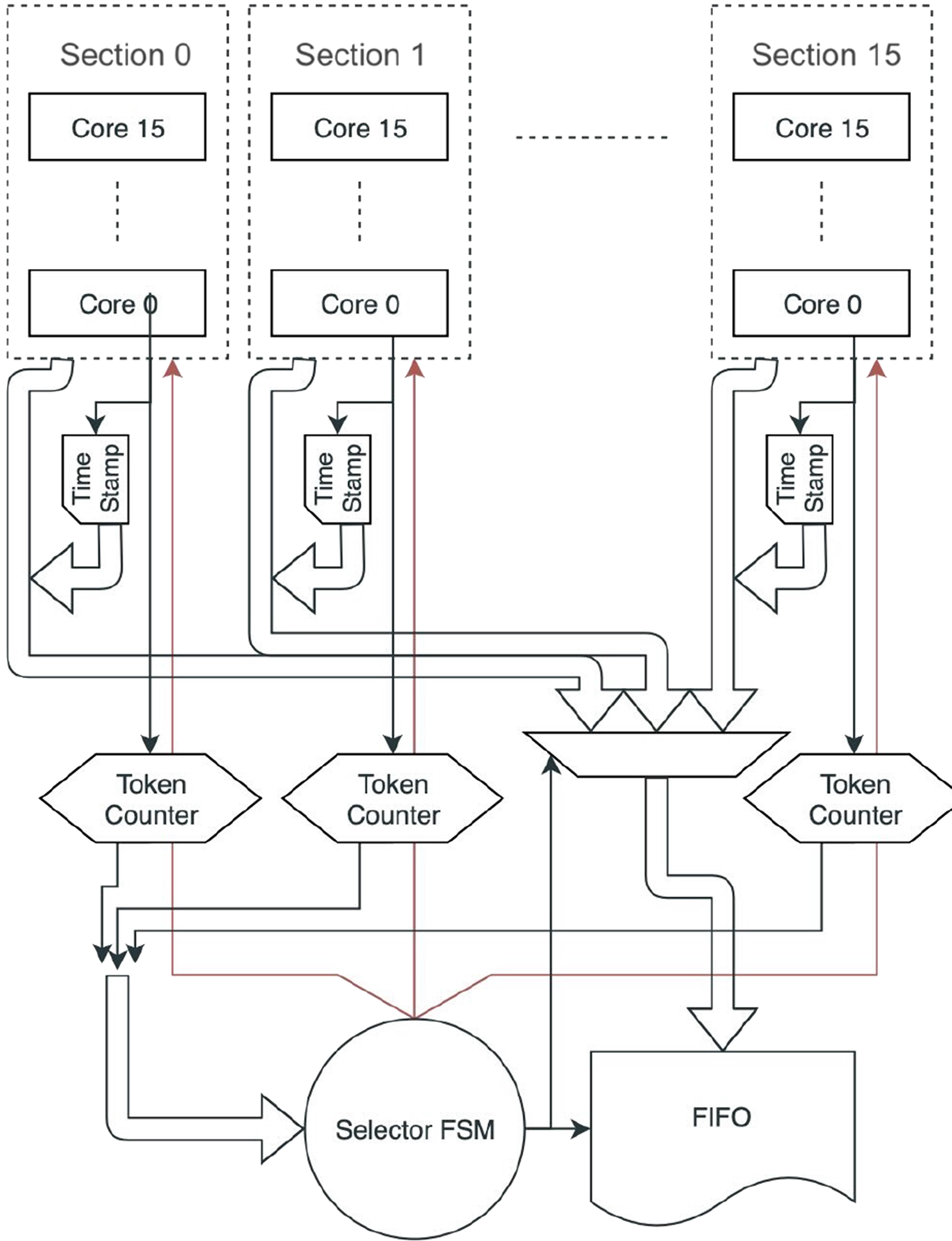
Block diagram of the ARCADIA-MD3 FD-MAPS section readout unit.
This low-power asynchronous architecture implements a readout logic where the system clock is not propagated to the pixel matrix. The clock is generated off-chip in a range of 100–320 MHz and is used by the double data rate (DDR) serializers and data transceivers, implemented with a custom high data rate and low-power data link (Pezzoli et al., 2021). The 32-bit data words are 8b10b encoded into 40-bit packets and, if the FIFO of the section readout unit is empty, synchronization packets are transmitted for keeping the clock aligned with the DAQ.
The periphery circuitry, FIFOs and readout units are designed such that a 100 MHz/cm2 particle hit rate can be handled and transmitted using 16 DDR output links. For very low power applications, the rate capability of the sensor is scaled down, and all data produced by the matrix is buffered from all section readout units into a central FIFO. The clock gating turns off the finite-state machines, encoders and serializers from all output links except one, and all but one of the c-LVDS data transceivers are disabled. Hence, the ARCADIA-MD3 chip can be configured to operate in a high or low rate mode (Figure 6). The power density of the full chip in low rate mode is approximately 10 mW/cm2. Depending on the driving strength settings for the c-LVDS links, which can be configured with 3-bit global configuration registers, the total power density of the chip operating in high rate mode is 17–30 mW/cm2.
FIGURE 6
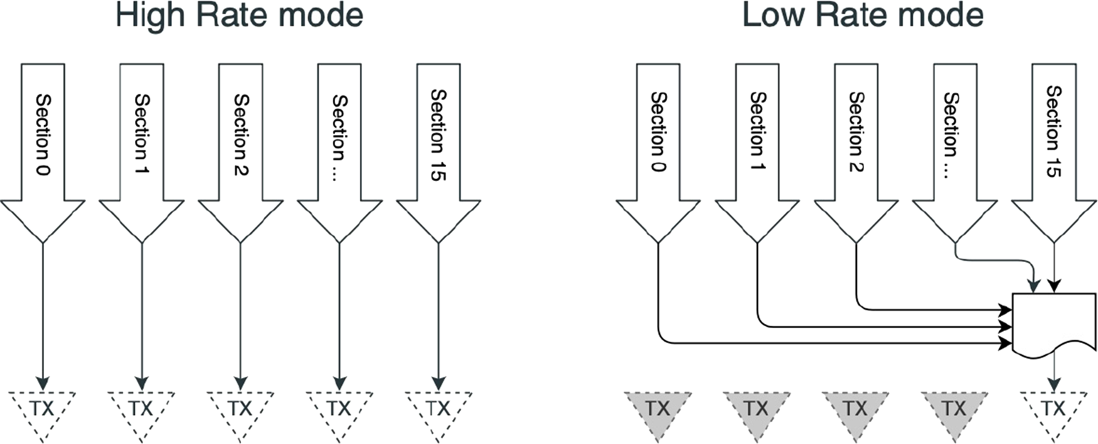
ARCADIA-MD3 FD-MAPS normal and low-rate operation modes.
The ARCADIA-MD3 FDMAPS, which is seen mounted on a front-end carrier board in Figure 7, was extensively tested using radioactive sources and in cosmic ray stands. A detailed description of the analog and digital circuits and electrical characterisation of the CMOS sensor and the results of a test beam characterisation with a three-plane telescope using the 120 GeV proton beam at FNAL will be discussed in detail in forthcoming publications in preparation.
FIGURE 7
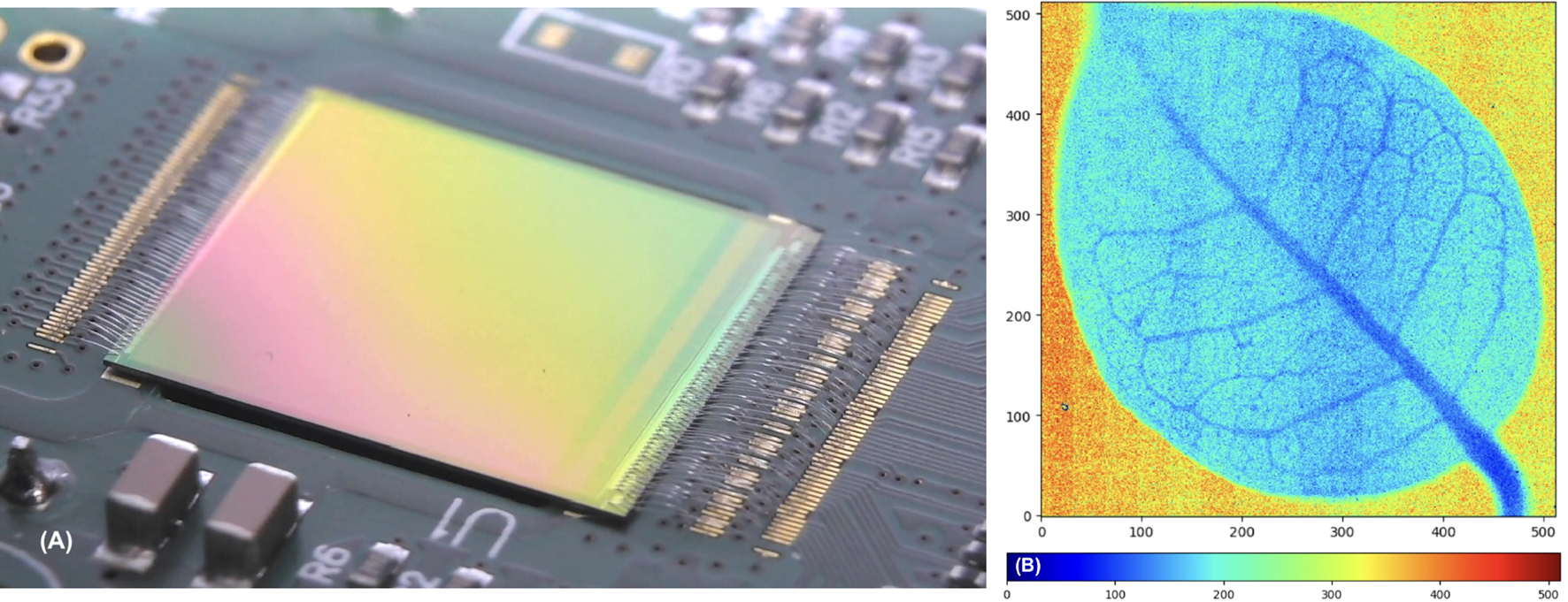
ARCADIA-MD3 FD-MAPS mounted on a PCB. Image of a leaf obtained with an X-ray radioactive source (55Fe) and a thick 512 × 512 pixel MD3 sensor; color bar indicates the number of counts on each pixel.
5 Conclusion
The ARCADIA collaboration developed a technology platform for the design and production of fully depleted CMOS monolithic sensors using a proprietary INFN-LFoundry sensor technology. This development, financed by an INFN CSN5 Open Call, allowed for the design and production of the ARCADIA-MD3 system-grade 515 × 512 FD-MAPS demonstrator with a very low power consumption, monolithic CMOS silicon strip arrays with embedded electronics, prototype chips for X-ray imaging and medical applications, and the implementation of a CMOS LGAD sensor concept for future timing detectors. The possibility to fully deplete very thick high-resistive silicon substrates paves the way for the use of these sensors in future medical instruments for proton, X-ray, molecular, and nuclear imaging, while the unprecedented power density of makes thinner ARCADIA sensors an excellent candidate for vertexing and tracking detectors on future leptonic colliders. The demonstration of the possibility of adding a gain layer for charge multiplication creates a CMOS-LGAD variation of the sensor, the excellent intrinsic timing performance of which can be exploited for time-of-flight detection in high-energy physics and many other applications requiring ultimate time resolution.
Statements
Author contributions
MD: Writing – original draft. AA: Writing – review and editing. GA: Writing – review and editing. FA: Writing – review and editing. GB: Writing – review and editing. G-FD: Writing – review and editing. ToC: Writing – review and editing. MC: Writing – review and editing. DC: Writing – review and editing. ThC: Writing – review and editing. SD: Writing – review and editing. DF: Writing – review and editing. AG: Writing – review and editing. PG: Writing – review and editing. SG: Writing – review and editing. RI: Writing – review and editing. MM: Writing – review and editing. SM: Writing – review and editing. CN: Writing – review and editing. LP: Writing – review and editing. DP: Writing – review and editing. AP: Writing – review and editing. MP: Writing – review and editing. PP: Writing – review and editing. LR: Writing – review and editing. ER: Writing – review and editing, Investigation. AR: Writing – review and editing. RS: Writing – review and editing. GT: Writing – review and editing. JW: Writing – review and editing.
Funding
The author(s) declare that financial support was received for the research and/or publication of this article. This work has received funding from INFN CSN5 under the Call 2018 project ARCADIA.
Conflict of interest
The authors declare that the research was conducted in the absence of any commercial or financial relationships that could be construed as a potential conflict of interest.
The author(s) declared that they were an editorial board member of Frontiers at the time of submission. This had no impact on the peer review process and the final decision.
Generative AI statement
The author(s) declare that no Generative AI was used in the creation of this manuscript.
Publisher’s note
All claims expressed in this article are solely those of the authors and do not necessarily represent those of their affiliated organizations, or those of the publisher, the editors and the reviewers. Any product that may be evaluated in this article, or claim that may be made by its manufacturer, is not guaranteed or endorsed by the publisher.
Footnotes
1.^ARCADIA Advanced Readout CMOS Architectures with Depleted Integrated sensor Arrays.
References
1
Arai Y. Miyoshi T. Kurachi I. (2017). “SOI monolithic pixel technology for radiation image sensor,” in 2017 IEEE International Electron Devices Meeting (IEDM), San Francisco, CA, USA, 02-06 December 2017 (IEEE), 16.2.1–16.2.4. 10.1109/IEDM.2017.8268401
2
Barbanera M. Silvestre G. Ambrosi G. Cossio F. Rolo M. D. D. R. Duranti M. et al (2024). Tests and characterization of a mixed-signal read out ASIC for silicon micro-strip detectors. Nucl. Instrum. Methods Phys. Res. Sect. A Accel. Spectrom. Detect. Assoc. Equip.1069, 169835. 10.1016/j.nima.2024.169835
3
Bianco E. (2021). “A LDO-based distributed power management system for high voltage CMOS sensors,” in 2021 IEEE Nuclear Science Symposium and Medical Imaging Conference (NSS/MIC), Piscataway, NJ, USA, 16–23 October 2021 (IEEE), 1–4. 10.1109/NSS/MIC44867.2021.9875620
4
Bui T. N. H. Large M. Poder J. Bucci J. Bianco E. Giampaolo R. A. et al (2024). Preliminary characterization of an active cmos pad detector for tracking and dosimetry in hdr brachytherapy. Sensors24, 692. 10.3390/s24020692
5
Burkhalter S. Caminada L. Ebrahimi A. Erdmann W. Kästli H.-C. Meier B. et al (2024). “MoTiC: prototype of a depleted monolithic pixel detector with timing,” in VERTEX2023 (PoS), 044. 10.22323/1.448.0044
6
Cai J. (2024). “Design of the readout chip with multi-energy bins for spectroscopic X-ray imaging,”. Ph.D. thesis (Politecnico di Torino). Available online at: https://iris.polito.it/handle/11583/2989620.
7
Corradino T. Neubüser C. Giovanazzi G. Andrini G. Ferrero C. Gioachin G. et al (2024). Simulation and first characterization of MAPS test structures with gain for timing applications. J. Instrum.19, C02036. 10.1088/1748-0221/19/02/C02036
8
De Cilladi L. Corradino T. Dalla Betta G.-F. Neubüser C. Pancheri L. (2021). Fully depleted monolithic active microstrip sensors: TCAD simulation study of an innovative design concept. Sensors21, 1990. 10.3390/s21061990
9
Durando S. (2021). “Ultra-low power discrete-time readout for CMOS radiation sensors,” in 2021 IEEE Nuclear Science Symposium and Medical Imaging Conference (NSS/MIC), Piscataway, NJ, USA, 16–23 October 2021 (IEEE), 1–3. 10.1109/NSS/MIC44867.2021.9875722
10
Durando S. Follo U. (2023). “Design and characterization of HERMES a discrete-time electronics CMOS sensor prototype in 110 nm for timing applications,” in 2023 IEEE Nuclear Science Symposium, Medical Imaging Conference and International Symposium on Room-Temperature Semiconductor Detectors (NSS MIC RTSD), Vancouver, BC, Canada, 04–11 November 2023 (IEEE), 1–3. 10.1109/NSSMICRTSD49126.2023.10338753
11
Ferrero C. ALICE Collaboration (2024). Validation of the 65 nm TPSCo CMOS imaging technology for the ALICE ITS3. J. Instrum.19, C04043. 10.1088/1748-0221/19/04/C04043
12
Ferrero C. Neubüser C. Pancheri L. Rivetti A. (2023). “Monte Carlo simulations of fully depleted CMOS pixel sensors for radiation detection applications,” in 2023 18th Conference on Ph.D Research in Microelectronics and Electronics (PRIME), Valencia, Spain, 18–21 June 2023 (IEEE), 101–104. 10.1109/PRIME58259.2023.10161878
13
Follo U. Gioachin G. Ferrero C. Mandurrino M. Bregant M. Bufalino S. et al (2024). First results on monolithic CMOS detector with internal gain. J. Instrum.19, P07033. 10.1088/1748-0221/19/07/P07033
14
Giampaolo R. (2022). “A novel fully depleted monolithic active CMOS microstrip sensor,”. Ph.D. thesis (Politecnico di Torino). Available online at: https://iris.polito.it/handle/11583/2959959.
15
Hillemanns H. Aimo I. Bedda C. Cavicchioli C. Collu A. Giubilato P. et al (2013). “Radiation hardness and detector performance of new 180nm CMOS MAPS prototype test structures developed for the upgrade of the ALICE Inner Tracking System,” in 2013 IEEE Nuclear Science Symposium and Medical Imaging Conference (2013 NSS/MIC), Seoul, Korea (South), 27 October 2013–02 November 2013 (IEEE), 1–5. 10.1109/NSSMIC.2013.6829475
16
Neubüser C. Corradino T. Dalla Betta G.-F. De Cilladi L. Pancheri L. (2021). Sensor design optimization of innovative low-power, large area FD-MAPS for HEP and applied science. Front. Phys.9, 625401. 10.3389/fphy.2021.625401
17
Pancheri L. Giampaolo R. A. Salvo A. D. Mattiazzo S. Corradino T. Giubilato P. et al (2020). Fully depleted MAPS in 110-nm CMOS process with 100–300-μm active substrate. IEEE Trans. Electron Devices67, 2393–2399. 10.1109/TED.2020.2985639
18
Perić I. Andreazza A. Augustin H. Barbero M. Benoit M. Casanova R. et al (2021). High-voltage CMOS active pixel sensor. IEEE J. Solid-State Circuits56, 2488–2502. 10.1109/JSSC.2021.3061760
19
Pernegger H. Bates R. Buttar C. Dalla M. Hoorne J. v. Kugathasan T. et al (2017). First tests of a novel radiation hard CMOS sensor process for depleted monolithic active pixel sensors. J. Instrum.12, P06008. 10.1088/1748-0221/12/06/P06008
20
Pezzoli M. Gaioni L. Manghisoni M. Ratti L. Re V. Traversi G. (2021). “A 2 Gbps custom LVDS transceiver for the ARCADIA project,” in 2021 IEEE Nuclear Science Symposium and Medical Imaging Conference (NSS/MIC), Piscataway, NJ, USA, 16–23 October 2021 (IEEE), 1–4. 10.1109/NSS/MIC44867.2021.9875554
21
Ravasenga I. (2024). Results of the new MAPS-based ALICE inner tracker operations in the LHC Run 3. Nucl. Instrum. Methods Phys. Res. Sect. A Accel. Spectrom. Detect. Assoc. Equip.1064, 169311. 10.1016/j.nima.2024.169311
22
Traversi G. Falchieri D. Gaioni L. Manghisoni M. Pezzoli M. Ratti L. et al (2023). A radiation hard bandgap voltage reference for the ARCADIA project. J. Instrum.18, C01049. 10.1088/1748-0221/18/01/C01049
Summary
Keywords
CMOS, fully depleted monolithic sensor, ASIC, low-power architectures, semiconductor sensors, integrated circuits, VLSI
Citation
Da Rocha Rolo M, Andreazza A, Ambrosi G, Alfonsi F, Balbi G, Dalla Betta G-F, Croci T, Caccia M, Chiappara D, Corradino T, Durando S, Falchieri D, Gabrielli A, Giubilato P, Garbolino S, Iuppa R, Mandurrino M, Mattiazzo S, Neubüser C, Pancheri L, Pantano D, Paterno A, Pezzoli M, Placidi P, Ratti L, Ricci E, Rivetti A, Santoro R, Traversi G and Wyss J (2025) ARCADIA fully depleted CMOS MAPS development with LFoundry 110 nm CIS. Front. Sens. 6:1603755. doi: 10.3389/fsens.2025.1603755
Received
31 March 2025
Accepted
03 July 2025
Published
11 August 2025
Volume
6 - 2025
Edited by
Omid Kavehei, The University of Sydney, Australia
Reviewed by
Soumyajit Mandal, Brookhaven National Laboratory (DOE), United States
Massimo Minuti, Universities and Research, Italy
Updates
Copyright
© 2025 Da Rocha Rolo, Andreazza, Ambrosi, Alfonsi, Balbi, Dalla Betta, Croci, Caccia, Chiappara, Corradino, Durando, Falchieri, Gabrielli, Giubilato, Garbolino, Iuppa, Mandurrino, Mattiazzo, Neubüser, Pancheri, Pantano, Paterno, Pezzoli, Placidi, Ratti, Ricci, Rivetti, Santoro, Traversi and Wyss.
This is an open-access article distributed under the terms of the Creative Commons Attribution License (CC BY). The use, distribution or reproduction in other forums is permitted, provided the original author(s) and the copyright owner(s) are credited and that the original publication in this journal is cited, in accordance with accepted academic practice. No use, distribution or reproduction is permitted which does not comply with these terms.
*Correspondence: Manuel Da Rocha Rolo, darochar@to.infn.it
† Present address: Thomas Corradino, Fondazione Bruno Kessler (FBK), Trento, Italy
Disclaimer
All claims expressed in this article are solely those of the authors and do not necessarily represent those of their affiliated organizations, or those of the publisher, the editors and the reviewers. Any product that may be evaluated in this article or claim that may be made by its manufacturer is not guaranteed or endorsed by the publisher.