Abstract
This paper provides a comprehensive overview of recent advances in silicon sensors designed for 4D tracking. These devices are of particular relevance for the next-generation of high intensity collider experiments, where meeting stringent requirements in both spatial and temporal resolution, along with unprecedented levels of radiation hardness, will be crucial. Among the various sensor technologies under development, 3D silicon sensors have demonstrated the potential to satisfy all key performance criteria. The paper discusses the development and fabrication processes of these sensors, emphasizing their capability to deliver exceptional timing resolution and radiation tolerance. Methods adopted for their characterization and results obtained from recent experimental campaigns are presented and critically analyzed. Furthermore, the pivotal role of readout electronics in enabling high-precision timing performance is underscored.
1 Technical requirements in high-intensity 4D-tracking
The term 4D-tracking generally refers to a tracking technique involving the simultaneous measurement of a particle’s position and time of passage across sensor-equipped tracking planes. As defined, this technique does not specify the required precision for time and spatial measurements, nor does it consider the environmental and experimental conditions under which the measurements must be performed.
Several collider experiments—currently in the design phase (e.g., LHCb Upgrade 2), at the proposal stage (e.g., neutrino tagging in short- and long-baseline experiments), or in conceptual development (e.g., FCC-hh)—require operation at unprecedented intensity levels . This imposes exceptionally stringent requirements on the tracking systems, particularly in their innermost regions, representing a substantial leap beyond the specifications of currently operating vertex detectors. Key performance targets include a spatial resolution better than 10 µm and a time resolution better than 50 ps per single pixel and per single-particle hit, considering the complete readout chain (sensor, amplifier, discriminator, and Time-to-Digital Converter). Additionally, system-level challenges such as ultra-low jitter reference distribution over large detector areas must be addressed. The trackers must also sustain extreme radiation levels, approaching fluences of 1-MeV .
These requirements represent a paradigm shift compared to existing vertex detector designs and are particularly challenging given the strict system constraints, especially regarding power density (1–2 ). Such advancements should be regarded as the design and realization of a novel and powerful instrument for discovery in physics research, warranting a specific designation: the High Intensity 4-Dimensional Tracker (hereafter referred to as HI4DT).
The successful design of a HI4DT necessitates concurrent and coordinated progress in sensor development, microelectronics design, cooling systems, and precision mechanics. In this paper, we focus on developments in silicon sensors and associated electronics, summarizing recent results that demonstrate the feasibility of meeting these demanding requirements. These achievements represent a major step forward in paving the way for the realization of the HI4DT.
2 Materials and methods
2.1 3D silicon sensors
Sensors for the detection of charged particles and suitable for a HI4DT must primarily have very high intrinsic space-time resolution. As mentioned earlier, experimental requirements demand a spatial resolution better than 10 μm, as in the case of LHCb vertex detector for the Upgrade 2 of the experiment (scheduled to be operated from 2035) (LHCb Collaboration, 2024). A binary resolution of 10 µm requires a pixel size of approximately 35 µm. Such a pixel dimension would be not suitable for various technological reasons on the sensor side, which will be clarified below. With present technologies, it would be very difficult to match also on the front-end electronics side, for limited space with respect to the functionalities to be integrated. The pixel size is therefore usually increased to around 50 μm, while the needed spatial resolution is obtained using clever clustering techniques and/or calculating the barycenter of charge deposits within the cluster. While complicating data processing stages, such techniques can lead to sub-binary space resolutions (Bassi et al., 2023).
Concerning time resolution, a longer argument is needed. High time resolution in particle sensors can be reached leveraging on the amplitude of the induced current signal and on the speed in Charge Collection Time (CCT) on the electrodes. Most importantly, a fundamental property of high resolution sensors is collection time uniformity, which results in narrower time-of-arrival distributions. Small CCT requires reducing inter-electrode (bias to junction) distance d, which turns to be also highly beneficial for radiation robustness, minimizing the probability of charge trapping in radiation-induced reticular defects. In traditional planar sensors, d gives also the amount of charge deposited by Minimum Ionizing Particles (MIPs) by . For this reasons, in fast planar sensors (reduced d), a low-gain doped layer must be introduced to gather a sufficient amount of charge (LGADs) (Cartiglia et al., 2014). On the other hand, introduction of gain by doping makes the sensors more prone to radiation damage, due to radiation erosion of the gain layer itself, which lowers the gain and deteriorates the sensor timing performance. For this reason, present gain-based planar sensors hardly reach a radiation resistance of a few 1-MeV (Ferrero et al., 2019).
In summary, an ideal silicon sensor for high time resolution and high radiation resistance (above
1-MeV
) should have the following main properties:
1. Fast CCT, so possibly small d;
2. Maximum uniformity in CCT across the sensible volume;
3. Large amount of charge deposit;
4. Possibly, no gain by doping.
These important items are briefly quantified and analyzed below.
2.1.1 Charge amount, sensor thickness, no gain
The minimum amount of charge required for fast timing depends on the performance of the front-end electronics, which must also comply with system constraints. From a circuit design perspective, several solutions capable of achieving satisfactory timing performance can be envisioned (
Lai and Cossu, 2020;
Cossu and Lai, 2023). However, they all ultimately depend on three key parameters:
• The affordable power density, which determines the maximum bias current in the amplifying stage and, consequently, its Slew Rate;
• The capacitance of the pixel sensor, which impacts the Signal-to-Noise Ratio (SNR);
• The amplitude of the induced current signal (i.e., the total deposited charge over time).
Recent studies on front-end electronics for timing, can provide a clear picture on how these parameters affect the final time resolution. Such results are shown in Figure 1. A sensor capacitance in the typical range of 50–100 fF is considered, along with a power density of 1–2 . For a total target time resolution per pixel below 50 ps, it is safer to specify a combined sensor and front-end contribution better of 30 ps It can be seen that a time resolution of 30 ps rms is achieved with a charge amount not lower than 1.5-2 fC. Considering a of about 80 electron-hole pairs per µm, this corresponds to a minimum thickness in the range of 150–200 µm. Planar sensors having such thickness would have CCTs of several ns. In the following subsection we will show that such CCT cannot give resolutions better than several hundreds of ps.
FIGURE 1

Relationship between electronic jitter vs. total collected charge (left) and vs. sensor capacitance (right). Both plots are results from measurements on the Ignite-0 test prototype (The IGNITE Collaboration, 2024). A power consumption on front-end of 10 µW corresponds approximately to a power density of 1.5 . The left plot is taken at . For a satisfactory jitter at nominal power a is needed.
A simple and clever idea consists in decoupling the sensor thickness z from the electrode distance d (Parker et al., 1997), by building vertical (or 3-Dimensional) electrodes, thus inventing the so-called 3D silicon sensors. In this case, bias and junction electrodes are digged into silicon by the DRIE (Deep Reactive Ion Etching) technique (Laermer et al., 2015; Forcolin et al., 2020). This well-known idea opens the great advantage to allow “playing” with the electrode shape and the pixel cell geometry, so to optimize the pixel timing performance by design of its geometry. This is explained in the following sub-section.
2.1.2 CCT: fast and maximally uniform
3D silicon sensors can have considerably reduced inter-electrode distance d. For a given pixel geometry, the limiting factors in d are the fabrication process resolution and the pixel capacitance. Present fabrication techniques would allow d 10 µm. However, a larger size is typically used (20–30 µm) in order to limit pixel capacitance, which has a direct impact on time resolution, especially when strong power density constraints are imposed by the system.
Pixel geometry and electrode shape have paramount importance in deciding the final timing performance of the designed 3D pixels. As it is well known (Ramo, 1939; Schockley, 1938), the contribution to the induced current signal of a charge carrier drifting towards the readout electrode is given, in each point of its path, by the dot product:where is the carrier charge, the weighting field, and the drift velocity of the carrier. Carrier drift velocity is a known function of the electric field, from the low field regime, where its mobility is defined, up to full saturation regime at high electric field ( in silicon) (Sze et al., 2021). When sharp timing distribution are required, it is important not only to have fast signals (short CCT), but especially to ensure a uniform electric field across the full pixel volume and operate towards the velocity saturation regime as much as possible.
By leveraging the design flexibility of 3D silicon pixels, extensive and accurate studies can be carried out optimizing pixel timing performance for a given system-required pixel size, as for example, in (Lampis, 2023) and (Loi et al., 2025). Due to this specific feature, 3D sensors can also be referred to as geometric sensors.
2.1.3 Timing resolution vs. detection efficiency
In assessing the timing performance of pixel sensors, it is crucial to correlate timing measurements with a precise characterization of detection efficiency. The interdependence of these two characteristics must be complemented by ensuring maximal response uniformity across the entire detection volume. Due to their geometric feature, such property is of particular relevance in 3D sensors, where bias and junction electrodes can give different shape to the pixel volume and electric field.
The specific geometry adopted in the sensor design can lead to variations in the electric field intensity across different regions of a pixel, resulting in differences in the total charge collection time (CCT). In some cases, significant variations in response can occur within the same pixel. Depending on the characteristics of the front-end electronics, regions with low electric field may exhibit delayed signal formation or even fail to generate a detectable response, particularly if the field approaches a local zero or if the electronics are sensitive predominantly to the fast component of the induced signal. Consequently, if only the fast component of the signal or the fastest regions of the pixel are considered, the measured time resolution may be biased toward such contributions, neglecting the tails in the Time-of-Arrival distribution. This effectively corresponds to disregarding a substantial portion of the pixel volume and leads to a mischaracterization of the true detection performance.
This phenomenon can be effectively illustrated by comparing two extreme cases: the hexagonal columnar geometry and the squared trench geometry, the latter being the geometry adopted for the TimeSPOT sensors, as illustrated in Figure 2. It can be observed that, although the hexagonal geometry has a much faster region all around the central readout electrode, its time distribution has a much wider dispersion, due to the weak-field region in correspondence to its periphery. Although in average slower, the final rms resolution is strongly in favor of the trench geometry, being it more uniform across the full detection volume.
FIGURE 2

Comparison of timing performance between different geometries of 3D sensors (Loi, 2020). Left: Time-of-Arrival map of a columnar hexagonal geometry, obtained by TCT technique (IR laser). Center: Same measurement on a trench square geometry. White areas in the maps are not accessible by this technique, being covered by metal structures. The insets are the corresponding electric field maps, where blue dots are weak field areas. Right: Time of Arrival distributions for the same geometries.
Extensive studies of this kind have clearly indicated the trench geometry as the best one for timing, and encouraged for a fabrication and test campaign using such technology: the 3D-trench TimeSPOT sensors.
2.2 The TimeSPOT 3D-trench sensors
As an output of the studies just described, the optimal geometry chosen for fast timing applications has been the 3D-trench, which is shown in Figure 3. As of today, three batches of TimeSPOT 3D-trench sensors, with pixel size and shape described in the same Figure 3, have been produced by the Fondazione Bruno Kessler (FBK, Trento) on 6 wafers. They correspond to a clear evolution in production technology. The DRIE process is particularly stressful for the processed wafers, especially when several contiguous trenches must be fabricated. First wafers were fragile and tended to easily break during production. This suggested the practice to start producing a very low density of reticules: 11 per wafer (2019), which turned to be 18 in 2021, reaching then a full coverage of the wafer surface in the 2024 AIDAInnova batch, after dedicated improvements in the production process (Boscardin, 2025).
FIGURE 3

Different views of the TimeSPOT 3D-trench pixel (Lampis, 2023). (A) Geometry and sizes of the detection volume. (B) Doping concentrations. (C) Pixel layout. (D) SEM picture of a pixel array (courtesy FBK).
The wafers integrated a manifold of different small test-structures and medium-size pixel matrices. Test structures feature single, double, four pixels, and multi-pixels, organized in strips of tens of pixels short-circuited together for being read-out on single-channel amplifiers (see Section 2.3). Dedicated test structures allow an accurate characterization of pixels and have been used to gain a deep knowledge of the sensor behavior concerning time resolution and efficiency. In this respect, the direct comparison between simulation models and experimental results helped to gain great confidence and control about the sensor behavior and performance (Loi et al., 2021; Brundu et al., 2022; Brundu et al., 2021).
The wafers include also pixel matrices of different sizes: 256 × 256 pixels and 32 × 32 pixels (2019 batch); 32 × 32 pixels (2021 batch); 32 × 32, 64 × 64 and 128 × 128 pixels (2024, AIDAInnova batch). Matrices have been produced to test the production yield on large structures and develop suitable sensors for matrix readout, using dedicated ASICs with embedded high-resolution timing facilities under development (Cadeddu et al., 2023), (The IGNITE Collaboration, 2025).
2.3 TimeSPOT sensors and front-end electronics
The time resolution of the TimeSPOT sensors has already been proven to be better than 10 ps (see Section 2.4). This performance, however, is strongly dependent on the characteristics and performance of the electronic front-end stage used (Cossu et al., 2023). The interplay between sensor timing performance and electronic front-end has been studied in detail in Lai and Cossu (2020), Riegler and Rinella (2017), and Riegler (2025). In this paper a summarized report of such studies is given.
As previously noted, the charge collection time (CCT) can serve as a reliable indicator of the sensor’s intrinsic timing resolution. However, the extent to which this intrinsic performance can be achieved in practice is strongly dependent on the characteristics of the readout electronics. In this context, the conventional approach of summing the timing uncertainties of the sensor and front-end amplifier in quadrature, treating them as statistically independent, provides only an approximate description. In reality, the final timing resolution is strongly correlated with the operation of the front-end electronics.
In conventional tracking detectors, optimized for spatial resolution, charge collection efficiency is the primary concern. These systems typically employ relatively slow front-end amplifiers operating in charge-sensitive (integrating) mode (Charge Sensitive Amplifier–CSA). It can be shown that (Lai and Cossu (2020), Riegler and Rinella (2017) and Section 2.3.1), with a CSA, the best achievable time resolution corresponds to half the standard deviation of the CCT distribution.
While CSAs integrate the total charge made available in the detection process, in order to maximally exploit the sensor capabilities in terms of speed, a different approach is more convenient. This is possible using a Trans-Impedance-Amplifying (TIA) mode, where the amplifier capacitive feedback is minimized and the focus is moved to the fast current rise at the start of the inductive process on the collecting electrode. It has been demonstrated (
Lai and Cossu, 2020;
Cossu and Lai, 2023) that in TIA mode, the output time resolution can be lowered up to a smaller fraction of the standard deviation of the CCT distribution (
Figure 4). However, in this case other features become critical (
Cossu and Lai, 2023):
• The intrinsic bandwidth of the transistor technology used.
• The noise rejection capability of the front-end circuit. As shown in Figure 4, the possibility to lower the electronics jitter to a smaller fraction of the CCT standard deviation is possible only if the discrimination threshold can be sufficiently lowered. This is only possible in a low-noise design.
• An adequate power budget available, to ensure a high slew rate of the output signal against a relatively high sensor capacitance.
FIGURE 4

Relationship between sensor timing performance (standard deviation of collection time distribution) and final Analog Front End (AFE) time resolution . Left: Simulated CCT distribution of a TimeSPOT sensor. Right: Propagation coefficient (defined in Lai and Cossu (2020)) for different AFE integration times and different discriminator thresholds.
The TIA approach is therefore especially effective using intrinsically wide-band technologies, as Heterogeneous Bipolar Si-Ge Transistors (Si-Ge HBTs), having transition frequency of about 85 GHz. TimeSPOT has developed dedicated fast, discrete-component TIA front-ends for the characterization of the timing performance of its 3D-trench sensors (Cossu and Lai, 2023) both in laboratory and in test-beam campaigns. Such front-end electronics features a signal-to-noise ratio SNR 20 and an electronic jitter below 7 ps at 2 fC input charge. The amplifier rise time is shorter than 100 ps. The power consumption is about 70 mW/channel. The TimeSPOT board directly houses and biases the sensors under test, which are wire-bonded to the amplifier input pads.
Si-Ge HBTs are also being used in integrated pixel systems (Milanesio et al., 2024). However, the design of a HI4DT apparatus is extremely complex, imposing hard system constraints, which necessarily become decisive in establishing the performance limit of the whole readout chain and in deciding specific technological choices. This issues are addressed in the next subsection.
2.3.1 TimeSPOT electronics and 4D-tracking systems
Integrated electronics for HI4DT have very demanding performance requirements, especially because they must be satisfied within very strict system constraints. Each readout channel, or electronics pixel, should integrate an amplifier and a fast discriminator. To sustain typical hit rates per pixel above 100 kHz, a Time-to-Digital-Converter (TDC) circuit with due precision (10 ps) and limited conversion time (1 µs) should also be integrated per single channel or shared among a small group of channels (2–8 typically).
Among the several system constraints, the most significant is the limited power budget allowed per electronics pixel. This is technically motivated by the present maximum technical capability to dissipate the power produced in a highly-integrated system, that is around 2 (LHCb, 2021). Compared to fast-TIA solutions used in the characterization of a small number of channels (Analog Front End–AFE–rise time around 100 ps), a reduced-bandwidth approach appears mandatory, allowing less current consumption, accepting a larger amount of signal integration, and a much longer rise time (Charge-Sensitive-Amplifier, AFE rise time of 5–10 ns). While it entails a slight performance degradation compared to the intrinsic timing capability of 3D-trench sensors, a Charge-Sensitive Amplifier (CSA) can still achieve a target resolution below 30 ps. This is demonstrated in detail in Lai and Cossu (2020) and is concisely illustrated in Figure 4. The plots show the estimated relationship between the intrinsic sensor timing performance, expressed by the average and standard deviation of its CCT distribution (left) and the final AFE time resolution . This relationship can be expressed as a fraction of the sensor , and depends on both the integration time of the AFE and the discriminator threshold applied. The values of correspond to the CSA approach. As said above, and shown in Figure 4, the ideal obtainable by a CSA is , which in the case of our sensor (3D-trench) is about 26 ps. Further improvement of the final could require an increase in power consumption, to get .
If 3D-trench silicon sensors are used, capable of an intrinsic 10 ps, the native sensor contribution to time measurement uncertainty tends to be negligible: the largely dominant limitation to system performance is represented by the electronics stage, which now becomes the main technical challenge concerning the final performance of our tracking device.
Developments on integrated electronics for 4D-tracking have started in the last couple of years. The particle physics community is decidedly oriented towards the choice of the CMOS 28-nm technology node for the next decade of developments in the field (Lai, 2022). This choice is mainly due to the need to adopt a technology with superior integration capability and higher resistance to radiation doses, compared to the previously used node (CMOS 65 nm) (CDS, 2020), which is manifestly unsuitable to integrate also timing capabilities at the pixel level. Characterization studies on CMOS 28-nm technology have shown resistance to doses greater than 1 Grad, whenever suitable design precautions are adopted (De Matteis, 2020).
The TimeSPOT project has carried out the first development ever of a CMOS 28-nm pixel readout ASIC for a HI4DT. This is a small-size prototype ASIC, named Timespot1, featuring a pixel matrix, a 55 µm pitch and about 3 mm2 of sensitive area (Cadeddu et al., 2023; Lai, 2022). Although still a preliminary implementation, the Timespot1 have demonstrated the technical possibility to limit the time jitter at the AFE level below 30 ps within the power budget of 20 µW per channel. Furthermore, the Timespot1 ASIC development has clearly emphasized the hard technical challenge represented by the implementation of a large area ASIC ( 2 cm2), capable to ensure a time resolution better than 50 ps in each pixel with the required low power budget. The Timespot1 shows an unacceptable dispersion in the timing performance values across its 1,024 pixels (Figure 5). This clearly demonstrates the need of superior accuracy in the distributions of the clock and power lines, which must be kept under strict control even at the level of small areas.
FIGURE 5
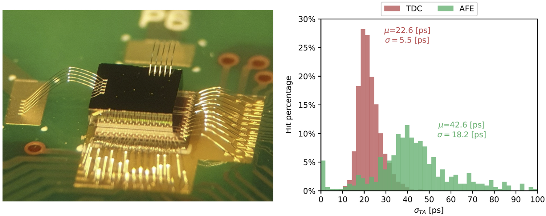
Left: The Timespot1 ASIC hybridized to a 3D-trench pixel matrix (placed on top). Right: Distribution of time resolutions , acquired on test-bench, for the time arrival measured at the output of the Analog Front End and on the TDC only. The jitter performance on the AFE, although satisfactory in average, ranges on from 10 ps to 100 ps.
The challenge for a large area timing ASIC for HI4DT is therefore still open. The ASIC developments initiated in the TimeSPOT project are being further pursued and refined within the INFN IGNITE project (The IGNITE Collaboration, 2025). A parallel CERN project, named LA-Picopix is also ongoing (Lopart, 2024). They have both the same target, which is being pursued with two alternative design approaches. Results are expected to arrive in the next couple of years.
2.4 Main results on 3D-trench sensors
The results obtained on TimeSPOT 3D sensor batches have been extensively and deeply described in several papers and conference talks (Brundu et al., 2021; Anderlini et al., 2020; Borgato et al., 2023; Borgato et al., 2024; Addison et al., 2024; Lai and Lampis, 2025). The reader is therefore invited to refer to those publications for any specific detail. However, it can be useful to summarize them here, emphasizing some features of particular relevance.
2.4.1 3D-trench sensors before irradiation
Before irradiation 3D-trench TimeSPOT pixels show a typical leakage current pA per pixel ( µm2) at room temperature, up to 100 V reverse bias. The breakdown voltage is typically above 150 V reverse bias (Forcolin et al., 2020).
Being the ohmic and junction electrodes not sensitive to MIPs, 3D-trench sensors have a geometrical inefficiency in detection of around 20% at 0° tilt angle , corresponding to a perpendicular impinging direction with respect to the sensor surface. Such inefficiency is gradually recovered while the tilting angle is increased and is taken below 1% at 20° (Figure 7).
Typical time of arrival (ToA) distributions are obtained with a fast TIA front-end, and using a time reference with resolution around 5 ps rms, based on MCP-PMT1 devices. ToA distributions are slightly asymmetrical, presenting a small shoulder towards slower ToAs (see Figure 6). The measured time distributions can be perfectly fitted with two Gaussian curves, a bulk (fast) Gaussian and a correction (slow) Gaussian. A physical interpretation of such two-Gaussian behavior can also be given, assigning the slow Gaussian to entries of the restricted area of low-field contributions inside the pixel volume (refer also to the ToA map in Figure 2.Center). Such interpretation is confirmed by observing the shape of the time distributions for increasing tilt angles (Figure 6), which gradually become more symmetric with a possible single-Gaussian fit at large angles. Indeed, in a pixel operated at tilt angle above 15°, the timing contributions from the fastest and the slowest pixel regions are mixed, giving a more uniform response. TimeSPOT time resolutions are in any case quoted as an effective standard deviations , which is a suitable weighted average of the two gaussian curves used in the distribution fit (Borgato et al., 2023):where is the fraction of the core Gaussian and is defined as .
FIGURE 6

Time of arrival distributions at 50 V reverse bias and three different . At 20° the distribution is symmetric. An 20° is the optimal operating condition of a 3D-trench sensor.
All the results published to date about tests on few-pixel structures have been obtained with a fast-TIA front-end (Cossu and Lai, 2023). Such tests are aimed at characterizing the performance limit of the sensor in time resolution. Time distributions have been constructed by acquiring the front-end output waveforms on a 8 GHz analog bandwidth 20 GSa/s 4 channels digital oscilloscope, and performing numerical waveform analysis. Analysis results have been quoted after four different alternative techniques (Figure 7): LE (Leading edge), i.e., fixed numerical threshold on the TIA signal, with no amplitude (time walk) correction; LE with amplitude correction; Numerical CFD (Constant Fraction Discriminator); ARC (Amplitude-Rise time Compensation) technique, that is a CFD technique with additional correction for the signal slope (Cho and Chase, 1972). The latter type of analysis has been also called Reference analysis, because it gives the most precise result.
FIGURE 7

Performance of pre-irradiated TimeSPOT 3D-trench sensors. Left: Detection efficiency at different . At 20° . Center: Time distribution, showing ps at 100 V reverse bias. Right: Time resolution at different reverse bias voltages and using different analysis techniques (Borgato et al., 2023).
Typical characteristics observed in time resolution measurements include the following: all techniques reach their peak performance at reverse bias voltages above 20 V, beyond which only minor improvements of 1–2 ps are observed (Figure 7). This indicates a broad operational plateau for sensor timing performance, extending from 20 V up to 150 V reverse bias.
With fast readout electronics, time resolutions well below 30 ps are achieved even using a simple LE discrimination technique, without the need for additional corrections or analysis. Applying amplitude corrections (CFD) improves the resolution to below 20 ps. Further refinement techniques (ARC) sharpen the resolution to approximately 10 ps.
Considering that the measured electronic jitter for a MIP energy deposit is around 7 ps, it is reasonable to estimate the intrinsic time resolution of the sensor alone to be better than 8 ps.
2.4.2 3D-trench sensors after irradiation
Test structures from the two TimeSPOT batches underwent three irradiation campaigns. All were performed with neutrons at JSI (Ljubljana) at the Triga Mark II Reactor facility. They correspond to the following fluences
in units of
:
1. and ;
2. and ;
3. and .
The natural increase in leakage current caused by radiation is kept under control by operating the samples at temperatures below −20°C. Irradiated samples have been first tested with a red laser inside a climatic chamber, and then exposed to a beam at the CERN SPS (H8 beam line) being operated inside boxes cooled with dry ice. Details about the experimental setup can be found in Borgato et al. (2024).
The first step in testing irradiated samples involves compensating for the drop in Charge Collection Efficiency (CCE) due to charge trapping by increasing the bias voltage. A practical approach is to record amplitude spectra and use the Most Probable Value (MPV) from a non-irradiated sample as a reference. Full CCE recovery is considered achieved when the reference MPV is reached. A similar method can be applied to time resolution measurements, where the goal is to recover the pre-irradiation time resolution by increasing the reverse bias voltage. Results are illustrated in Figure 8.
FIGURE 8

Performance of irradiated TimeSPOT 3D-trench sensors. Time resolution at different reverse bias voltages and using different analysis techniques for four different fluences (Borgato et al., 2024; Addison et al., 2024).
Table 1 summarizes the results presented Borgato et al. (2024), Addison et al. (2024), and Lai and Lampis (2025). Tests at the two highest fluences were initiated in a climatic chamber but have not yet been completed. In fact, increasing the reverse bias voltage beyond 400 V was not tolerated by the front-end board, necessitating a specific redesign that is currently in progress. This also prevented the completion of meaningful timing tests, as full depletion of the detection volume could not be achieved. However, results obtained up to already demonstrate that 3D silicon sensors are fully operational at extreme fluences, even beyond the requirements of HI4DT experiments of the next-generation, while still keeping outstanding performance in time resolution and efficiency.
TABLE 1
| Fluences | Reverse bias [V] for nominal CCE | Reverse bias [V] for T. res ps | Notes |
|---|---|---|---|
| 0 | 20 | 20 | |
| 1 | 60 | 40 | |
| 2.5 | – | 50 | CCE not tested |
| 5 | 220 | 100 | |
| 10 | 270 | 150 | |
| 50 | 70% at 400 | NA | Preliminary |
| 100 | 30% at 400 | NA | Preliminary |
Operational reverse bias voltages vs. fluences. Fluences are given in units of .
3 Discussion
In this work it was shown a summary of the most relevant results obtained in the TimeSPOT project and in its immediate follow-ups. The TimeSPOT sensors and electronics have open a clear path towards the feasibility of High Intensity 4D Tracking, in the sense that have been specified above in the paper. Reaching the target timing performance below 50 ps per hit at the expected fluences of future experiments at colliders was not foregone before the TimeSPOT results. It can be said that the TimeSPOT technology has enabled this discovery path in fundamental research.
Such path has been enabled but is not yet concluded. Further developments are needed on 3D silicon sensor to improve production process and yield. On the other hand, integrated electronics still presents many issues to be solved about high resolution obtainable on large areas, while respecting very severe system constraints.
While also other research groups are attacking these problems, the TimeSPOT mission is evolving in the IGNITE project, which aims to solve the HI4DT challenge on the timing electronics side.
Statements
Author contributions
AL: Funding acquisition, Methodology, Writing – original draft, Investigation, Visualization, Validation, Conceptualization, Resources, Supervision, Project administration, Writing – review and editing.
Funding
The author(s) declare that financial support was received for the research and/or publication of this article. This work was supported by the Fifth Scientific Commission (CSN5) of the Italian National Institute for Nuclear Physics (INFN), within the Project TimeSPOT and by the ATTRACT-EU initiative, INSTANT project, funded by the European Union’s Horizon 2020 Research and Innovation program under GA no. 101004761.
Acknowledgments
The author wish to warmly thank all the members of the TimeSPOT collaboration for their enthusiastic and precious work in these exciting and successful years spent together in developing innovative tools for future discoveries.
Conflict of interest
The author declares that the research was conducted in the absence of any commercial or financial relationships that could be construed as a potential conflict of interest.
The author(s) declared that they were an editorial board member of Frontiers, at the time of submission. This had no impact on the peer review process and the final decision.
Generative AI statement
The author(s) declare that no Generative AI was used in the creation of this manuscript.
Publisher’s note
All claims expressed in this article are solely those of the authors and do not necessarily represent those of their affiliated organizations, or those of the publisher, the editors and the reviewers. Any product that may be evaluated in this article, or claim that may be made by its manufacturer, is not guaranteed or endorsed by the publisher.
Footnotes
1.^Micro Channel Plate - Photon Multiplier Tube
References
1
Addison M. Bellora A. Borgato F. Brundu D. Cardini A. Cossu G. M. et al (2024). Characterisation of 3D trench silicon pixel sensors irradiated at 1·1017 1 MeV neq cm−2. Front. Phys.12, 1497267. 10.3389/fphy.2024.1497267
2
Anderlini L. Aresti M. Bizzeti A. Boscardin M. Cardini A. Dalla Betta G. F. et al (2020). Intrinsic time resolution of 3D-trench silicon pixels for charged particle detection. J. Instrum.15, P09029. 10.1088/1748-0221/15/09/p09029
3
Bassi G. Giambastiani L. Hennessy K. Lazzari F. Morello M. Pajero T. et al (2023). A FPGA-based architecture for real-time cluster finding in the LHCb silicon pixel detector. IEEE Trans. Nucl. Sci.PP, 1189–1201. 10.1109/TNS.2023.3273600
4
Borgato F. Brundu D. Cardini A. Cossu G. M. Dalla Betta G. F. Garau M. et al (2023). Charged-particle timing with 10 ps accuracy using TimeSPOT 3D trench-type silicon pixels. Front. Phys.11. 10.3389/fphy.2023.1117575
5
Borgato F. Cardini A. Cossu G. M. Dalla Betta G. F. Garau M. La Delfa L. et al (2024). Characterisation of highly irradiated 3D trench silicon pixel sensors for 4D tracking with 10 ps timing accuracy. Front. Phys.12, 1393019. 10.3389/fphy.2024.1393019
6
Boscardin M. Ficorella F. Dalla Betta G.-F. Monreal L. P. Vignali M. C. Ali O. M. et al (2025). “Development and production of advanced 3D pixel sensors at FBK,” in Talk given at VCI (Vienna: VCI). Available online at: https://indico.cern.ch/event/1386009/contributions/6279095/.
7
Brundu D. Cardini A. Contu A. Cossu G. M. Dalla Betta G. F. Garau M. et al (2021). Accurate modelling of 3D-trench silicon sensor with enhanced timing performance and comparison with test beam measurements. J. Instrum.16, P09028. 10.1088/1748-0221/16/09/p09028
8
Brundu D. Contu A. Cossu G. M. Loi A. (2022). Modeling of solid state detectors using advanced multi-threading: the TCoDe and TFBoost simulation packages. Front. Phys.10, 804752. 10.3389/fphy.2022.804752
9
Cadeddu S. Frontini L. Lai A. Liberali V. Piccolo L. Rivetti A. et al (2023). Timespot1: a 28 nm CMOS pixel read-out ASIC for 4D tracking at high rates. J. Instrum.18, P03034. 10.1088/1748-0221/18/03/p03034
10
Cartiglia N. Baselga M. Dellacasa G. Ely S. Fadeyev V. Galloway Z. et al (2014). Performance of ultra-fast silicon detectors. J. Instrum.9, C02001. 10.1088/1748-0221/9/02/C02001
11
CDS (2020). RD53B users guide. Available online at: https://cds.cern.ch/record/2754251.
12
Cho Z. Chase R. (1972). Comparative study of the timing techniques currently employed with Ge detectors. Nucl. Instrum. Methods98, 335–347. 10.1016/0029-554X(72)90115-2
13
Cossu G. M. Brundu D. Lai A. (2023). Intrinsic timing properties of ideal 3D-trench silicon sensor with fast front-end electronics. J. Instrum.18, P07014. 10.1088/1748-0221/18/07/p07014
14
Cossu G. M. Lai A. (2023). Front-end electronics for timing with pico-second precision using 3D trench silicon sensors. J. Instrum.18, P01039. 10.1088/1748-0221/18/01/P01039
15
De Matteis M. Resta F. Pipino A. Fary F. Mattiazzo S. Enz C. et al (2020). 1-GRad-TID effects in 28-nm device study for rad-hard analog design. Cham: Springer International Publishing, 299–315. 10.1007/978-3-030-25267-0_18
16
Ferrero M. Arcidiacono R. Barozzi M. Boscardin M. Cartiglia N. Betta G. D. et al (2019). Radiation resistant LGAD design. Nucl. Instrum. Methods Phys. Res. Sect. A Accel. Spectrom. Detect. Assoc. Equip.919, 16–26. 10.1016/j.nima.2018.11.121
17
Forcolin G. Boscardin M. Ficorella F. Lai A. Loi A. Mendicino R. et al (2020). 3D trenched-electrode pixel sensors: design, technology and initial results. Nucl. Inst. Methods Phys. Res. Sect. A981, 164437. 10.1016/j.nima.2020.164437
18
Laermer F. Franssila S. Sainiemi L. Kolari K. (2015). “Chapter 21 - deep reactive Ion etching,” in Micro and nano technologies. Second edn. (Boston: William Andrew Publishing), 444–469. 10.1016/B978-0-323-29965-7.00021-X
19
Lai A. Cossu G. M. (2020). High-resolution timing electronics for fast pixel sensors. arXiv:2008.09867.
20
Lai A. Stabile A. Cardini A. Lampis A. Loi A. Piccolo L. et al (2022). TimeSPOT ASIC developments for 4D-tracking. in Talk given at “TWEPP 2022” (Bergen: CERN). Available online at: https://indico.cern.ch/event/1127562/contributions/4904519/.
21
Lai A. Cardini A. Bellora A. Lampis A. Loi A. Brundu D. et al (2025). “Could we efficiently operate 3D silicon pixel-based tracking detectors irradiated with neutron fluences up to 1E+18 1MeVneq/cm2?,” in Talk given at “VCI 2025” (Vienna: VCI). Available online at: https://indico.cern.ch/event/1386009/contributions/6279107/.
22
Lampis A. (2023). “Innovative silicon pixel sensors for a 4D VErtex LOcator detector for the LHCb high luminosity upgrade,”. PhD Thesis (Cagliari Univerity).
23
LHCb (2021). Framework TDR for the LHCb upgrade II. Available online at: http://cds.cern.ch/record/2776420.
24
LHCb Collaboration (2024). LHCb upgrade II scoping document. 10.17181/CERN.2RXP.HDK0
25
Loi A. (2020). “Design and test of a timing optimized 3D silicon sensor for HL-HLC experiments,”. PhD Thesis (Cagliari Univerity).
26
Loi A. Contu A. Lai A. (2021). Timing optimisation and analysis in the design of 3D silicon sensors: the TCoDe simulator. JINST16, P02011. 10.1088/1748-0221/16/02/P02011
27
Loi A. Lai A. Ye J. Dalla Betta G. F. (2025). Timing-optimised 3D silicon sensor with columnar electrode geometry. Sensors25, 926. 10.3390/s25030926
28
Lopart X. (2024). The LA-Picopix project. Available online at: https://indico.cern.ch/event/1456663/contributions/6184370/attachments/2954032/5193546/PicoPix_DRD4.pdf.
29
Milanesio M. Paolozzi L. Moretti T. Latshaw A. Bonacina L. Cardella R. et al (2024). Time resolution of a SiGe BiCMOS monolithic silicon pixel detector without internal gain layer with a femtosecond laser. J. Instrum.19, P04029. 10.1088/1748-0221/19/04/p04029
30
Parker S. Kenney C. Segal J. (1997). 3D — a proposed new architecture for solid-state radiation detectors. Nucl. Instrum. Meth. A395, 328–343. 10.1016/S0168-9002(97)00694-3
31
Ramo S. (1939). Currents induced by electron motion. Proc. IRE27, 584–585. 10.1109/jrproc.1939.228757
32
Riegler W. (2025). Time resolution limits in silicon sensors from landau fluctuations and electronics noise.
33
Riegler W. Rinella G. A. (2017). Time resolution of silicon pixel sensors. J. Instrum.12, P11017. 10.1088/1748-0221/12/11/p11017
34
Schockley W. (1938). Currents to conductors induced by a moving point charge. J. Appl. Phys.9, 635–636. 10.1063/1.1710367
35
Sze S. M. Li Y. Ng K. K. (2021). Physics of semiconductor devices. John Wiley and Sons.
36
The IGNITE Collaboration (2024). “First results on the Ignite-0 test ASIC in CMOS 28-nm technology,” in Talk given by GM Cossu at TWEPP 2024 (Glasgow: CERN). Available online at: https://indico.cern.ch/event/1381495/contributions/5988499/.
37
The IGNITE Collaboration (2025). “Results and perspectives of the IGNITE project on CMOS 28-nm technology ASICs,” in Talk given by A. Lai at VCI (Vienna: VCI). Available online at: https://indico.cern.ch/event/1386009/contributions/6279114/.
Summary
Keywords
particle tracking detectors, solid-state detectors, timing detectors, high time resolution, high luminosity
Citation
Lai A (2025) TimeSPOT developments on charged-particle silicon sensors for high intensity 4D-Tracking. Front. Sens. 6:1619719. doi: 10.3389/fsens.2025.1619719
Received
28 April 2025
Accepted
26 June 2025
Published
21 July 2025
Volume
6 - 2025
Edited by
Alberto Quaranta, University of Trento, Italy
Reviewed by
Massimo Minuti, Ministry of Education, Italy
Angela Kok, SINTEF Digital, Norway
Updates
Copyright
© 2025 Lai.
This is an open-access article distributed under the terms of the Creative Commons Attribution License (CC BY). The use, distribution or reproduction in other forums is permitted, provided the original author(s) and the copyright owner(s) are credited and that the original publication in this journal is cited, in accordance with accepted academic practice. No use, distribution or reproduction is permitted which does not comply with these terms.
*Correspondence: A. Lai, adriano.lai@ca.infn.it
Disclaimer
All claims expressed in this article are solely those of the authors and do not necessarily represent those of their affiliated organizations, or those of the publisher, the editors and the reviewers. Any product that may be evaluated in this article or claim that may be made by its manufacturer is not guaranteed or endorsed by the publisher.