 Roberto R. Rivera-Durón
 Ricardo Sevilla-Escoboza2
- 1Unmanned System Research Institute, Northwestern Polytechnical University, Xi'an, China
- 2Centro Universitario de los Lagos, Universidad de Guadalajara, Lagos de Moreno, Mexico
- 3College of Transportation, Chang'an University, Xi'an, China
The obtainment of a dynamical logic gate (DLG), which is a device capable of implementing several logic functions using the same model, has been one of the goals of the scientific community. Dynamical systems, specifically those that display chaotic behavior, have been widely used to emulate different logic gates which are the basis of general-purpose computing. In this study, we present a methodology based on unstable dissipative systems of type 1 (UDS-1), a kind of dynamical system capable of generating multi-scrolls and multi-stability. Using these two features, we codify inputs, subsequently, we get the adequate output, developing in this way a dynamical (reconfigurable) logic gate that performs any of the sixteen possible logic functions of two inputs. A highlight of the proposed methodology is that the selection of the desired logic gate is realized just by varying a couple of parameters.
1. Introduction
In the last decades, a vast quantity of budget and effort has been invested to design and construct a unique device capable of implementing several logic gates into the same structure. In 1998, Sinha and Ditto showed the capacity of lattices of coupled logistic maps to emulate NOR gates, resulting in chaos computing [1]. From this pioneering study, several schemes have been exploited, these include chaotic continuous and discrete dynamical systems [2–7]; piece-wise linear (PWL) systems [8, 9]; resonators controlled by noise intensity [10]; cellular neuronal networks [11]; memristive devices [12, 13], and doping-free bipolar junction transistors controlled by polarity [14]. In chaos computing, chaotic elements are exploited to act as different logic functions by changing parameters so that these devices are more flexible than the silicon-based architectures.
On the other hand, multi-stability is intrinsically present in physics, chemistry, biology, among other fields [15]. It is defined as the coexistence of multiple possible final stable states. The final state to which the system will converge depends on the initial conditions [16]. In the dynamical systems field, multi-stability is an important feature related to dissipative systems. Unstable dissipative systems are those that have a focus-saddle equilibrium point responsible for stable and unstable manifolds, but also, the sum of their eigenvalues is negative [17].
In most of the previously presented approaches related to chaos computing, the sensitivity to the initial conditions of chaotic elements is exploited to obtain logic gates; however, it could be a disadvantage when an experimental implementation is realized due to small variations in the voltages or a little differences in the tolerance of components. In this study, we present a methodology based on the capacity of displaying multi-stability of unstable dissipative systems of type 1 (UDS-1) to implement a dynamical logic gate (DLG), also known as a reconfigurable logic gate. In our proposed method, logic zeros and logic ones are codified through one of the clearly distinguishable possible final states of the multi-stable USD-1. Although we obtain logic gates using multi-stability, which is closely related to the initial conditions, we take advantage of the concept of the basin of attraction, so that a vast set of initial conditions will produce the same response in our system. This gives the advantage to our model of being easily reliable and repeatable. An important aspect of our methodology is that by just varying two parameters, we can get the complete spectrum of two-input logic functions (16 logic gates), which represents an advantage in terms of time and resources for the future electronic implementation of the model.
The remaining of this article is structured as follows: In Section 2, we provide the fundamental theory of UDS-1. Our proposed methodology is explained in Section 3. Results for the DLG are shown and discussed in Section 4. Finally, in Section 5, some conclusions about this article are given.
2. Unstable Dissipative Systems Fundamentals
In the same spirit of Campos-Cantón et al. [18], let us consider the following dynamical system:
where is the state vector, denotes a linear operator and it is a non-singular matrix. Also, let Λ = {λ1, λ2, λ3} be the set of eigenvalues of matrix A.
The system given by Equation (1) is called an UDS-1, if the following two statements are satisfied:
1. Focus-saddle equilibrium condition. The matrix A must possess one negative pure real eigenvalue λ1, whereas λ2,3 are complex conjugate with a positive real part.
2. Dissipativity condition. The system is dissipative, if .
Moreover, a UDS-1 is capable of displaying multi-scrolls if an adequate commutation control law is applied to it. A simple way to generate multi-scrolls consists of applying a PWL function to modify the system dynamics by changing the position of equilibrium points. Thus, if an additive term B is applied to Equation (1), it can be rewritten as:
where is a real vector, and it works as a discrete commutation function dependent on the state x. B changes depending on which domain the trajectory is located. The main idea is dividing the full phase space into domains, in other words, . With this last regard, and supposing , then the switching function is given by:
Because A is a non-singular matrix, the equilibrium point of the system given by Equation (2) is located at x* = −A−1B. Specifically, equilibrium points are with i = 1, 2, …, k. In this way, the system will have as equilibrium points as domains are defined.
3. Methods
In order to design a DLG, we start considering the following system in its canonical form:
whose eigenvalues are Λ = {λ1 = −0.6358, λ2 = 0.0679 + 0.8842i, λ3 = 0.0679 + 0.8842i}; and . Thus, system of Equation (4) satisfies the two conditions mentioned in Section 2 to classify it as a USD-1.
The next step in our methodology consists of forcing the system in Equation (4) to generate n scrolls. It is important to mention that the number of scrolls n to be generated can be arbitrarily chosen and increased, the only requirement is that n ≥ 2. In our case, we decide to generate three scrolls. Therefore, we add the commutation vector B to Equation (4) and we can rewrite it as:
as we desire to generate three scrolls, then the same quantity of equilibrium points are necessary and we want them arbitrarily located at , which are equispaced only along the x1 plane. Also, let us remember that each equilibrium point is located in , this leads to . Hence, we need to define the switching function b3 and each βi, which are described as:
where the commutation surfaces among domains are located at -1.5 and 1.5 to preserve the shape and symmetry of the scrolls.
Up to now, we have constructed a UDS-1 with the capability of generating three scrolls. In Figure 1 are plotted projections of the states of the system given by Equations (5) and (6) for several planes. The plot in Figure 1A corresponds to the x1x2 plane, where it is possible to distinguish the three scrolls clearly. Figure 1B is the projection onto the x1x3 plane; whereas Figure 1C shows the projection in the x2x3 plane.
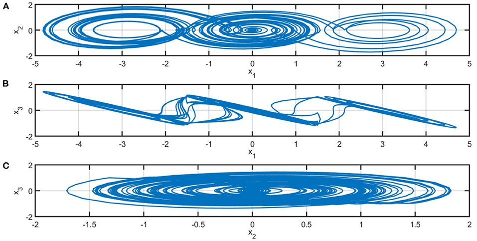
Figure 1. Projections of the system given by equations. axplusbmethod and b3method onto the planes of R3. The plot (A) corresponds to x1x2 plane; (B) is the projection onto x1x3 plane; and (C) is the projection in x2x3 plane.
The following step is controlling the system described by Equations (5) and (6) with the aim of transforming it into a multi-stable system. To achieve this goal, first, let us define the negative reciprocal of element a33 as μ = −1/a33, and second, let us multiply the last row of matrix A and the switching function b3 times μ.
The parameter μ induces multi-stability to the system but leaves the dissipativity unchanged. Now, each scroll we previously generated with the system described by Equations (5) and (6) have become a possible final stable state to which the system will converge depending on the initial conditions. In other words, the system will converge to one of these three scrolls depending on whether its initial condition belongs to the basin of attraction of the scroll. Figure 2 shows these possible final states to which the system can converge. Figure 2A corresponds to the initial condition x(0) = (−2.5, −1, 0); Figure 2B to x(0) = (1.1, −1, 0); and finally, Figure 2C to x(0) = (2.5, −1, 0).
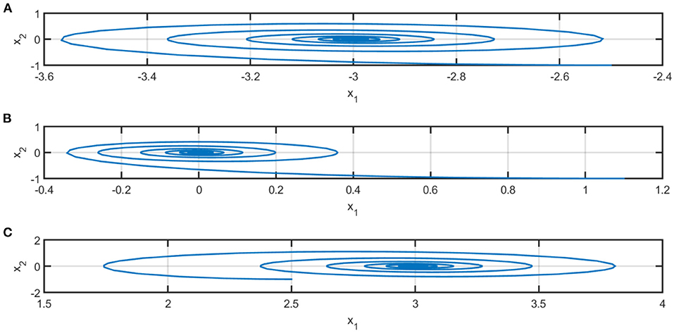
Figure 2. Projections onto the x1x2 plane of the three final possible attractors of the multi-stable system of equation (7). axplusbmultimethod. Plot (A) corresponds to the initial condition x(0) = (−2.5, −1, 0); Plot (B) to x(0) = (1.1, −1, 0); and Plot (C) to x(0) = (2.5, −1, 0).
To develop a system capable of emulating all possible two-input logic functions, we have built a simple three-node network in which each node is a multi-stable UDS-1 governed by Equation (7). The topology of this network is shown in Figure 3. Node 1 and node 2 act as inputs, whereas node 3 works as the output of the DLG. In the example, we are using to explain our methodology, the number of scrolls matches with the number of nodes in the network, but there is no relationship between these two quantities.
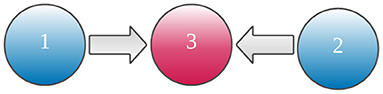
Figure 3. Topology of the three-node network used to develop a dynamical logic gate (DLG).
As it was previously explained, the multi-stable UDS-1 of Equation (7) can converge to three final attractors depending on the initial conditions, in such a way that we can choose two of these attractors to codify logical zeros and ones. Arbitrarily, we decide that if the multi-stable UDS-1 is converging to the left attractor (Figure 2A), then it will represent a logical zero. On the other hand, if the multi-stable UDS-1 is converging to the right attractor (Figure 2C), then this will be coded as a logical one. The initial condition (x0, y0, z0) = (−3, 0, 0) and (x0, y0, z0) = (3, 0, 0) belong to the basin of attraction of the left and right attractor, respectively. Thus, we can define the target point (x, y, z) = (I1,2 ∈ {−3, 3}, 0.001, 0) to be reached through feedback control. Taking these assumptions into consideration, the dynamics of node 1 acting as the first input is described by:
where the switching function bn1 is:
The dynamics of node 2 which works as the second input is given by:
whose commutation function is:
How input node 1 and node 2 interconnect with the output node 3 considers the following linear affined system:
where is a column vector whose elements I1,2 ∈ {−3, 3}; and γ ∈ ℝ are system parameters to be adjusted to obtain the desired logic gate. Function h results from summing the scalar product α·i plus an offset given by γ. The output of the system is ruled by:
where κ ∈ ℝ is defined as a threshold.
Therefore, the dynamics of node 3 behaving as output is governed by:
with the function bn3 governed by:
The networked system described by Equations (10)–(19) emulates any of the possible sixteen two-input logic functions whose truth tables appear in Table 1. ⊥ represents the contradiction or null; I1I2, AND; , inhibition of I2; I1, transfer of I1; , inhibition of I1; I2, transfer of I2; I1 ⊕ I2, XOR; I1+I2, OR; , NOR; , XNOR; , complement of I2; , implication (I2 implies I1); , complement of I1; , implication (I1 implies I2); , NAND; ⊤, tautology or identity.
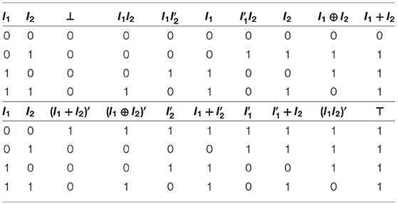
Table 1. Truth tables for all the sixteen possible two-input logic functions expressed in Boolean variables (0 and 1).
The selection of logic gate functionality is realized by adjusting system parameters α1, α2, γ, and κ so that Equations (16) and (17) are satisfied simultaneously. Depending on the values of I1 and I2, Equation (16) will have one of the results shown in the third column of Table 2. These results will fall or will not be inside the interval (−κ, κ) according to the truth table of the desired logic function we desire to obtain. If h of Equation (16) falls in the open interval (−κ, κ) defined in Equation (17), then I3 = 3 which represents a logical one and the output node 3 will converge to the left attractor; otherwise, I3 = −3 what is defined as a logical zero and the output node 3 will converge to the right attractor.
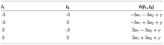
Table 2. Values of h(I1, I2) in Equation 16.
In the following lines, we briefly explain the selection of parameters for the case of the AND (I1I2) gate, but an analog procedure is necessary for the rest of the logic gates. First, we fix the threshold κ = 3. According to the truth table of AND gate shown in the fourth upper column of Table 1, only when I1 = 3 and I2 = 3, the sum h must fall inside the interval (−3, 3); the remaining combinations of I1 and I2 will fall outside (−3, 3). In such a way, the following inequalities must be accomplished simultaneously:
After algebraic calculations, it is possible to determine that α1 = 0.3, α2 = 0.5, and γ = −4.0 are one of the several combinations that satisfy the corresponding inequalities in the system Equation (20).
4. Results
The parameter selection is not unique, there are several combinations of α1, α2, γ, and κ that can satisfy Equations (16) and (17). For this reason, we utilized a computer code to determine the set of system parameters to obtain each of the sixteen two-input logic functions for a constant value of κ = 3. After inspecting the results, we noticed that the value of α1 = 0.3 appeared in all the cases, therefore, we can assume that α1 is constant too. This last represents an advantage because the functionality of the DLG only depends on the values of α2 and γ, which can result in the optimization of time and resources in the future experimental realization of the DLG. A map for parameters α2 and γ to select functionality of DLG is shown in Figure 4. The complete list of the system parameters that we used to emulate each logic function is shown in Table 3, it is important to remark that in all the cases κ = 3 and α1 = 0.3.

Figure 4. Map of regions for parameters α2 and γ of DLG.
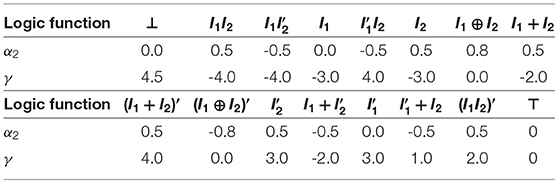
Table 3. List of the system parameters α2 and γ used to emulate each logic function.
We can compare our proposal with respect to other approaches to measure the benefits between the achieved logic gates and the number of parameters to be configured. In this sense, Table 4 shows a comparative frame among previously presented studies and our proposal of DLG. From this table, it is possible to observe that [10] achieves only a pair of logic gates (AND, OR) by varying the resonator's operation parameters. The study in Peng et al. [8] obtains seven logic gates (⊥, AND, OR, NAND, NOR, XOR, ⊤) by tuning three parameters. Eleven logic gates (⊥, AND, OR, NAND, NOR, XNOR, I2, , , , ⊤) were achieved in Li et al. [7] by varying a single parameter. Special mention deserves the work done in Peng et al. [9], in which authors got all the possible two-input logic gates as well as we did in our approach through the tuning of a pair of parameters.
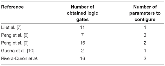
Table 4. Comparative frame among several approaches already presented and our proposal of DLG.
Numerical simulations were realized to prove the correct performance of the developed DLG. We started simulations letting the three nodes behave freely so that μ = 1 and they are not in a multi-stable regime for time 0 ≤ t ≤ 500. Then, we set μ = −1/0.5 to get multi-stability in all the nodes, and we configured I1 of node 1 to be I1 = −3 for 500 < t ≤ 1500 and I1 = 3 for 1500 < t ≤ 2500; in analogous way, I2 of the node 2 was configured to be I2 = −3 for t ∈ {(500, 1000] ∪ (1500, 2000]}, and I2 = 3 for t ∈ {(1000, 1500] ∪ (2000, 2500]}. In this way, the four possible combinations of I1 and I2 shown in the first two columns of Table 2 were accomplished. The plots of the temporal evolution of the input node 1 are shown in Figures 5A, 6A, whereas the plots in Figures 5B, 6B correspond to the temporal evolution of input node 2. The behavior of the output node 3 is plotted in Figures 5, 6. ⊥ is represented in Figure 5C; I1I2 in Figure 5D; in Figure 5E; I1 in Figure 5F; in Figure 5G; I2 in Figure 5H; I1 ⊕ I2 in Figure 5I; I1+I2 in Figure 5J; in Figure 6C; in Figure 6D; in Figure 6E; in Figure 6F; in Figure 6G; in Figure 6H; in Figure 6I; ⊤ in Figure 6J. From Figures 5, 6 is possible to note the fast response time of the output node, this is because of the control law we added which yields the system to an initial condition into the basin of attraction of the desired attractor but also, this control law avoids falling in any of the equilibrium points of the system.
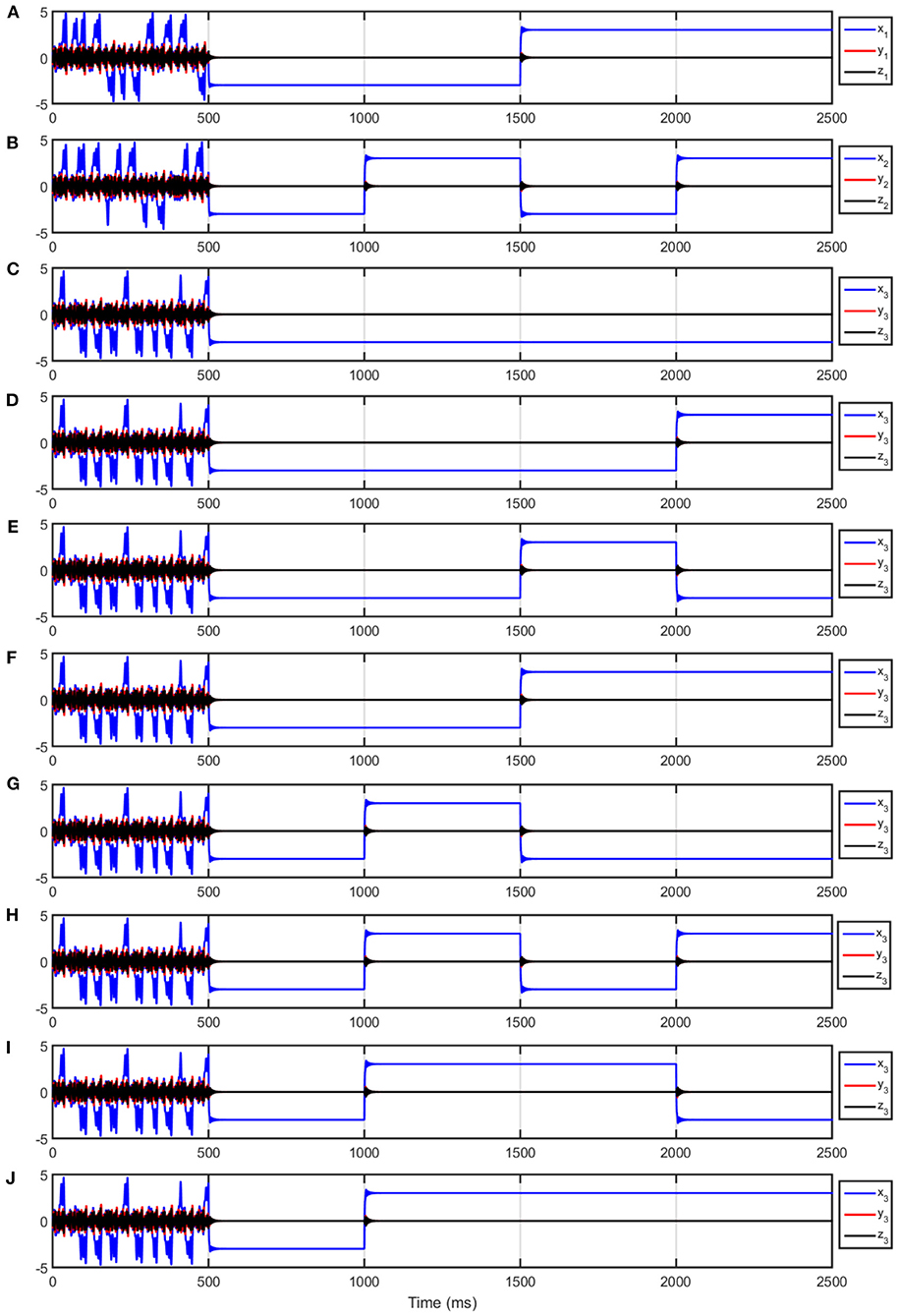
Figure 5. Temporal evolution of the input nodes and for the output node emulating the logic functions shown in the upper part of Table Truth Tables. The plot in (A) corresponds to the input node 1. Plot (B) corresponds to the temporal evolution of input node 2. bot is represented in plot (C); I1I2 in plot (D); I1I2' in plot (E); I1 in plot (F); I1'I2 in plot (G); I2 in plot (H); I1 plus I2 in plot (I); I1+I2 in plot (J).
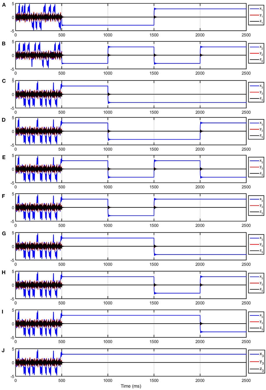
Figure 6. Temporal evolution of the input nodes and for the output node emulating the logic functions shown in the lower part of Table TruthTables. The plot in (A) corresponds to the input node 1. Plot (B) corresponds to the temporal evolution of input node 2. (I1+I2)' in plot (C); (I1 ⊕ I2)' in plot (D); I2' in plot (E); I1 + I2' in plot (F); I1' in plot (G); I1' + I2 in plot (H); (I1I2)' in plot (I); top in plot (J).
Now, let us implement a full adder to prove the performance of the DLG when it is executing compound functions. The full adder is a combinational circuit that realizes the arithmetical sum of three bits. I1 and I2 are the bits to be added, whereas Cin is the input carry bit coming from a previous sum. Due to the sum of three bits varies from 0 to 3, the circuit needs two bits to correctly represent the addition; these bits are S and Cout, which are the sum and the output carry, respectively. The truth table for the full adder is shown in Table 5. From the truth table is possible to determine the logic functions S = Cin ⊕ I1 ⊕ I2 and Cout = CinI1+CinI2+I1I2. The logic diagram to configure the full adder consists of seven logic gates (G1 to G7), and it is displayed in Figure 7. Again, we launched the numerical simulations with all the nodes behaving freely so that μ = 1 and they are not in a multi-stable regime for time 0 ≤ t ≤ 250, after this time, we set μ = −1/0.5 to get multi-stability in all the nodes. To achieve the eight possible combinations in the inputs of the full adder, we proceeded as follows: first, we configured Cin at node 1 to be Cin = −3 for 250 < t ≤ 1250 and Cin = 3 for 1250 < t ≤ 2250; second, I1 at the node 2 was configured to be I1 = −3 for t ∈ {(250, 750] ∪ (1250, 1750]}, and I1 = 3 for t ∈ {(750, 1250] ∪ (1750, 2250]}; finally, I2 at node 3 was fixed to be I2 = −3 for t ∈ {(250, 500] ∪ (750, 1000] ∪ (1250, 1500] ∪ (1750, 2000]}, and I2 = 3 for t ∈ {(500, 750] ∪ (1000, 1250] ∪ (1500, 1750] ∪ (2000, 2250]}. The temporal evolution of the full adder is plotted in Figure 8. The plots in Figures 8A–C correspond to Cin, I1, and I2, respectively. Figure 8D displays the behavior of G1 which is configured as XOR gate (I1 ⊕ I2). Figure 8E shows the evolution of the AND gate G2 (I1I2). In Figure 8F is plotted the AND gate G3 (I1Cin). Figure 8G is showing the evolution of the AND gate G4 (I2Cin). Figure 8H shows the temporal evolution of G5 configured as OR gate and which receives in its inputs the signals coming from G2 and G3. The signal coming from G4 and G5 are received by G6 and whose output corresponds to Cout, this is shown in Figure 8I. Finally, G7 processes the signal coming from G1 and Cin and its output results in the sum S, which is plotted in Figure 8J.
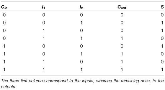
Table 5. The truth table for the full adder.
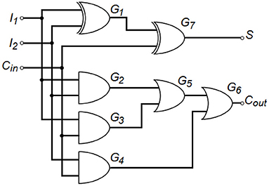
Figure 7. Logic diagram of the full adder whose truth table is shown in Table 5.
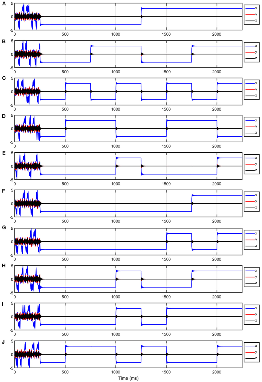
Figure 8. Temporal evolution of the nodes in the full adder. The plot (A) corresponds to Cin; (B) to I1; (C) to I2; (D) to G1; (E) to G2; (F) to G3; (G) to G4; (H) to G5; (I) to G6 which is Cout; and (J) to G7 which is the sum S.
Our proposal of DLG can be taken into an electronic realization through currently available electronic components. Since the core of DLG is composed of three ordinary differential equations, they can be implemented using operational amplifiers (OP-AMP) in the basic configurations (integrator, inverted adder, and inverted), resistors, and capacitors. From an engineering viewpoint, the computational complexity and hardware cost to implement a DLG through a three-node network could be elevated compared with the current logic devices. For this reason, we have as future work to achieve the same results here reported but just using a single UDS-1 for each DLG, which will decrease the prices and the design tasks. However, our approach has the advantage that the programming to implement several functions can be quite quick and it can be done on the fly. Also, another advantage we can elucidate is related to a research issue; whereas in the traditional digital logic devices, as the FPGAs, the states updating is governed by a master clock so that the updating occurs in a synchronous way; in our device, we can add a delay element to investigate autonomous Boolean networks, a kind of dynamical system where the state updating happens when there exists a transition in any input. In this way, we can study the effect of delays in autonomous Boolean networks.
5. Conclusion
We presented a methodology to design a DLG using a multi-stable UDS-1. We constructed a three-node network of multi-stable UDS-1. In this topology, a couple of nodes act as inputs of the logic gate, whereas the remaining node is the output or response. Using a pair of the different final states (attractors) of the multi-stable system, we were able to codify Boolean ones and zeros, and subsequently, we obtain the adequate response to emulate all the possible two-input logic functions (16 logic gates). We are sure that our results are relevant because we just need to adjust a pair of parameters to select the functionality of the DLG, this could be important in terms of time and cost in the future experimental realization of this DLG.
Data Availability Statement
The original contributions presented in the study are included in the article/supplementary material, further inquiries can be directed to the corresponding author/s.
Author Contributions
RR-D was involved in methodology conceptualization, numerical simulations, writing the original draft, reviewing and editing the manuscript. RS-E is responsible for numerical simulations, validation, reviewing and editing the manuscript. Q-LW responsible for numerical simulations, validation, data visualization, and reviewing and editing the manuscript. All authors contributed to the article and approved the submitted version.
Funding
RS-E acknowledges support from Consejo Nacional de Ciencia y Tecnología call SEP-CONACYT/CB-2016-01, grant number 285909.
Conflict of Interest
The authors declare that the research was conducted in the absence of any commercial or financial relationships that could be construed as a potential conflict of interest.
Publisher's Note
All claims expressed in this article are solely those of the authors and do not necessarily represent those of their affiliated organizations, or those of the publisher, the editors and the reviewers. Any product that may be evaluated in this article, or claim that may be made by its manufacturer, is not guaranteed or endorsed by the publisher.
References
2. Sinha S, Ditto W. Computing with distributed chaos. Phys Rev E. (1999) 60:363–77. doi: 10.1103/PhysRevE.60.363
3. Munakata T, Sinha S, Ditto W. Chaos computing: implementation of fundamental logical gates by chaotic elements. IEEE Trans Circ Syst I Fundam Theory Appl. (2002) 49:1629–33. doi: 10.1109/TCSI.2002.804551
4. Murali K, Sinha S, Ditto W. Implementation of NOR gate by a chaotic chua's circuit. Int J Bifurcat Chaos. (2003) 13:2669–72. doi: 10.1142/S0218127403008053
5. Murali K, Sinha S, Ditto W. Construction of a reconfigurable dynamic logic cell. Pramana. (2005) 64:433–41. doi: 10.1007/BF02704569
6. Murali K, Miliotis A, Ditto W, Sinha S. Logic from nonlinear dynamical evolution. Phys Lett A. (2009) 373:1346–51. doi: 10.1016/j.physleta.2009.02.026
7. Li L, Yang C, Hui S, Yu W, Kurths J, Peng H, et al. A reconfigurable logic cell based on a simple dynamical system. Math Probl Eng. (2013) 2013:735189. doi: 10.1155/2013/735189
8. Peng H, Yang Y, Li L, Luo H. Harnessing piecewise-linear systems to construct dynamic logic architecture. Chaos Interdiscipl J Nonlin Sci. (2008) 18:033101. doi: 10.1063/1.2953494
9. Peng H, Liu F, Li L, Yang Y, Wang X. Dynamic logic architecture based on piecewise-linear systems. Phys Lett A. (2010) 374:1450–6. doi: 10.1063/5.0046968
10. Guerra D, Bulsara A, Ditto W, Sinha S, Murali K, Mohanty P. A noise-assisted reprogrammable nanomechanical logic gate. Nano Lett. (2010) 10:1168–71. doi: 10.1021/nl9034175
11. Yuan X, Liu W. Implementation and improvement of dynamic logic gates based on cellular neural networks. In: 2012 Fifth International Workshop on Chaos-fractals Theories and Applications. (Dalian) (2012). p. 99–103.
12. Rothenbuhler A, Tran T, Smith E, Saxena V, Campbell K. Reconfigurable threshold logic gates using memristive devices. In: 2012 IEEE Subthreshold Microelectronics Conference (SubVT). Waltham, MA (2012). p. 1–3.
13. James A, Krestinskaya O, Maan A. Recursive threshold logica bioinspired reconfigurable dynamic logic system with crossbar arrays. IEEE Trans Biomed Circ Syst. (2020) 14: 1311–22. doi: 10.1109/TBCAS.2020.3027554
14. Sahu A, Kumar A, Tiwari S. Performance investigation of universal gates and ring oscillator using doping-free bipolar junction transistor. In: 2020 IEEE Silicon Nanoelectronics Workshop (SNW). Honolulu, HI (2020). p. 125–6.
15. Hens C, Dana S, Feudel U. Extreme multistability: attractor manipulation and robustness. Chaos Interdiscipl J Nonlin Sci. (2015) 25:053112. doi: 10.1063/1.4921351
16. Pisarchik A, Feudel U. Control of multistability. Phys Rep. (2014) 540:167–218. doi: 10.1016/j.physrep.2014.02.007
17. Campos-Cantón E, Femat R, Chen G. Attractors generated from switching unstable dissipative systems. Chaos: Interdis J Nonlin Sci. (2012) 22:033121. doi: 10.1063/1.4742338
Keywords: unstable dissipative systems, multi-stability, reconfigurable computing, reconfigurable logic gate, dynamical logic gate
Citation: Rivera-Durón RR, Sevilla-Escoboza R and Wang Q-L (2022) Generation of a Dynamical Logic Gate From Unstable Dissipative Systems of Type 1. Front. Appl. Math. Stat. 8:877006. doi: 10.3389/fams.2022.877006
Received: 16 February 2022; Accepted: 10 March 2022;
Published: 25 April 2022.
Edited by:
Cristiana J. Silva, University of Aveiro, PortugalReviewed by:
Jesus Manuel Munoz-Pacheco, Benemérita Universidad Autónoma de Puebla, MexicoViet-Thanh Pham, Ton Duc Thang University, Vietnam
Copyright © 2022 Rivera-Durón, Sevilla-Escoboza and Wang. This is an open-access article distributed under the terms of the Creative Commons Attribution License (CC BY). The use, distribution or reproduction in other forums is permitted, provided the original author(s) and the copyright owner(s) are credited and that the original publication in this journal is cited, in accordance with accepted academic practice. No use, distribution or reproduction is permitted which does not comply with these terms.
*Correspondence: Roberto R. Rivera-Durón, cnJyZHJuQGdtYWlsLmNvbQ==