 Curtis D. Lee
 Ellis Meng
- 1Department of Biomedical Engineering, University of Southern California, Los Angeles, CA, USA
- 2Ming Hsieh Department of Electrical Engineering, University of Southern California, Los Angeles, CA, USA
Structures and testing methods for measuring the adhesion strength, minimum bending diameter, and bending fatigue performance of thin-film polymer electronic architectures were developed and applied to Parylene–metal–Parylene systems with and without the moisture barrier Al2O3 [deposited using atomic layer deposition (ALD)]. Parylene–metal–Parylene interfaces had the strongest average peel test strength and Parylene–Parylene interfaces had the weakest peel test strength. Layers of ALD Al2O3 deposited within the device increased the average peel strength for Parylene–Parylene interfaces when combined with silane A-174, but did not increase that of the Parylene–metal–Parylene interface. Metal traces in the middle of 24 μm thick Parylene–metal–Parylene devices had a minimum bending diameter of ~130 μm before breaking and being measured as an open circuit. The addition of one layer of Al2O3 above the traces allowed them to be completely creased when bent away from the Al2O3 layer without producing an open circuit, but increased the minimum bending diameter to ~450 μm when bent towards the Al2O3. Although fatigue testing produced cracks in all devices after 100k bends, the insulation of the Parylene–metal–Parylene devices without Al2O3 performed well with electrochemical impedance spectroscopy showing only small decreases in impedance magnitude and small increases of impedance phase at low frequencies. However, devices with Al2O3 failed during EIS due to Al2O3 being deteriorated by water.
Introduction
Unlike traditional silicon-based electronics, thin-film polymeric devices are inherently flexible, which is important for devices targeting soft, moving tissues for various applications, such as monitoring electrical activity from muscles, measuring nerve impulses from the central or peripheral nervous system, and delivering therapeutic electric current, such as in pacemakers, deep brain stimulation, cochlear implants, and spinal cord stimulation. For such applications, flexibility is required to maintain good contact (important for sensing weak electrical signals and reducing the amount of current required for a therapeutic effect) and avoid damaging tissue through tethering effects.
In addition, thin-film polymeric devices use photolithography and other technologies borrowed from the semiconductor industry to pattern electrodes or other sensors or structures onto the surfaces of materials, such as Parylene (Johnson and Wise, 2012; Kuo et al., 2013; Zhao et al., 2013), polyimide (Kisban et al., 2009; Tolstosheeva et al., 2011; Viventi et al., 2010), or polydimethylsiloxane (Gray et al., 2004; Guo et al., 2014). Because thin-film polymeric devices are based on microfabrication technology used to make transistors or micro-sensors, these devices have micron-scale resolution or better and allow sensors, such as transistors (Nomura et al., 2004) or force sensors (Gutierrez et al., 2010), to be integrated directly onto the flexible device. These devices are thin enough to be rolled up and delivered via catheter (Fonseca et al., 2006) or incorporated into the catheter itself (Li et al., 2008a). Thin-film polymeric devices for cochlear stimulation (Johnson and Wise, 2010), spinal cord stimulation (Rodger et al., 2007) as well as electrocardiography (ECG) (Viventi et al., 2010; Yu et al., 2012), electrocorticography (ECOG) (Toda et al., 2011), and intracortical neural recordings (Kim et al., 2013) have been demonstrated.
While thin-film polymeric devices are flexible, biocompatible, and allow for high resolution features, they are prone to delamination (Li et al., 2008b; Seymour et al., 2009) and carry concerns about their mechanical robustness (Schuettler et al., 2005). Mechanical tests for individual devices for specific applications have been performed, such as measuring the properties of a device while wrapping it around fixed-diameter structures (Chen et al., 2010; Kisban et al., 2009; Ochoa et al., 2013), fixing it to a moving tissue (Metallo et al., 2011; Viventi et al., 2010; Zhao et al., 2013), or allowing it to self-curl (Yamagiwa et al., 2013). In addition, tests have been performed to screen for methods to improve adhesion (Chang et al., 2011; Seymour et al., 2009). However, systematic studies that investigate in detail the mechanical performance and adhesion of multi-layer film stacks in generalized polymeric film devices are lacking in research literature.
Also, typical reports in literature present data from single devices (such as bend testing across cylinders of multiple diameters) from non-destructive experiments. Destructive and continuous peel/bend tests can provide specific limits to device performance. In this work, designs for polymeric thin-film devices and tests are presented as a way to determine the robustness of thin-film structures. In particular devices and tests to measure peel strength, minimum bending diameter, and bending fatigue characteristics of Parylene–metal–Parylene, structures are tested to determine their potential and limitations for use as thin-film devices. In addition, these devices and tests are used to measure the properties of Al2O3 [deposited using atomic layer deposition (ALD)], which – in combination with Parylene – has been shown to improve water-barrier properties of encapsulated silicon devices (Ghosh et al., 2005) and chosen in the present study to act as a water barrier and adhesion promoter for Parylene–metal–Parylene devices.
Materials and Methods
Table 1 summarizes the distinct test structure designs for measuring the peel strength, minimum bending diameter, and bending fatigue. Subsequent sections describe details of the fabrication, design, and testing of these devices.
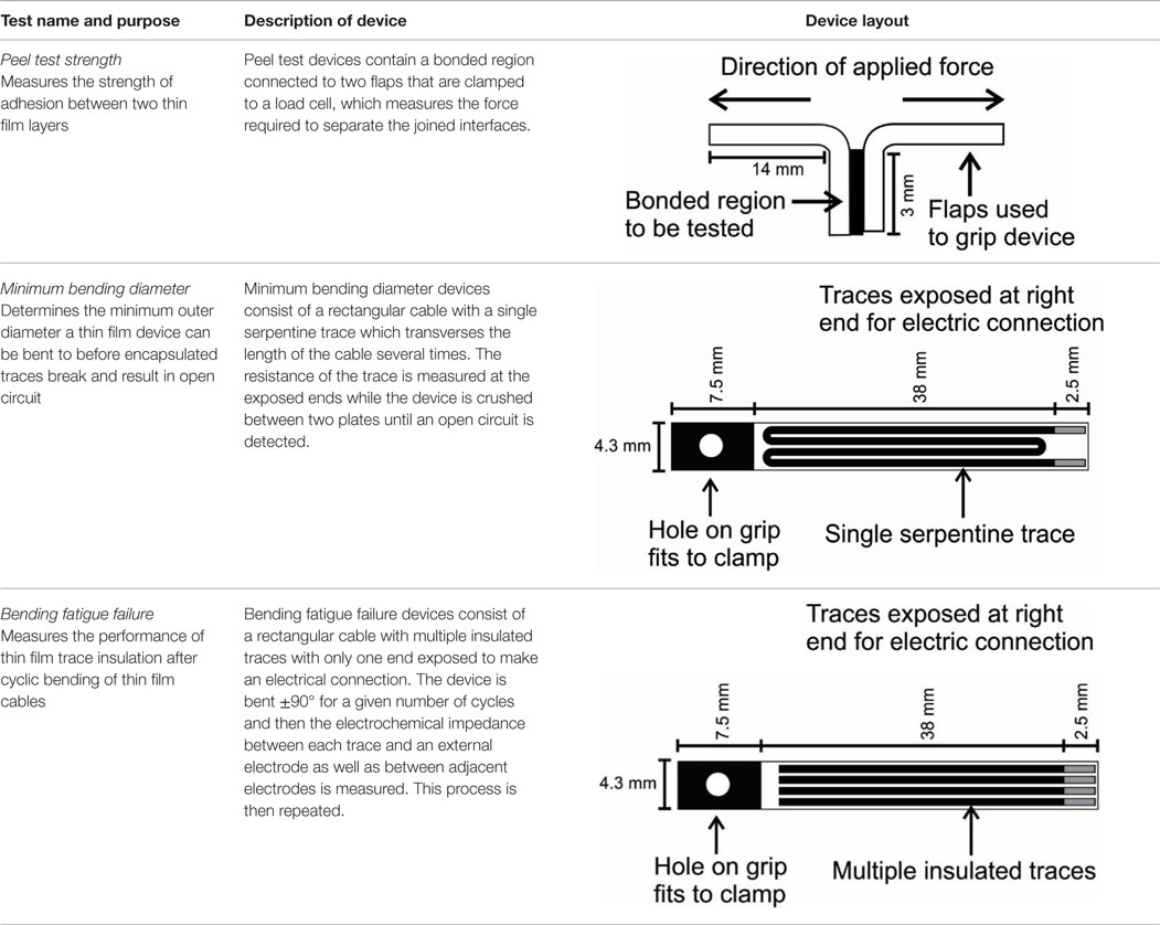
Table 1. Summary of devices and tests used to measure peel strength, minimum bending diameter, and bending fatigue.
Device Fabrication
Peel test, minimum bending diameter test, and bending fatigue test devices were all fabricated using similar fabrication methods (Figures S1A,B in Supplementary Material). Details of Parylene C-based thin-film devices can be found in previous publications (Kuo et al., 2013), therefore, only a brief description is given here. First, ~13 μm of Parylene C was deposited onto a prime silicon wafer using CVD (Specialty Coating Systems Inc., IN, USA). Next, standard photolithographic liftoff was used to pattern 200 nm of e-beam deposited Pt on top of the underlying Parylene C. Finally, a second layer of Parylene was deposited to insulate the Pt patterns, and O2 plasma was used to expose contact pads and cut out devices. ALD was used to deposit Al2O3 either before and after metal traces or only on top of metal traces (Figure S1B in Supplementary Material, details of Al2O3 given below in Section “Atomic Layer Deposition of Al2O3 Barrier”).
Atomic Layer Deposition of Al2O3 Barrier
Various processing techniques, such as thermoforming, cleaning, and chemical treatments, have been investigated to improve thin-film adhesion (Chang et al., 2011; Kim and Najafi, 2005). Also, barrier layers and adhesion promoters have been used to prevent failure of thin-film insulation (Xie et al., 2012; Xie et al., 2013). However, only static conditions were used to test for improved bond strength and insulation integrity. In the current study, ALD Al2O3 combined with the silane adhesion promoter A-174 was deposited between layers of Parylene to act as both a barrier layer and adhesion promoter. The effect of this layer, not only on adhesion promotion but also on trace performance in bending failure and bending fatigue, was measured.
Al2O3 has been shown to be an excellent barrier to water vapor (Ghosh et al., 2005) and for this reason was deposited with Parylene to improve the performance of implanted neural electrodes (Xie et al., 2013). Parylene serves as a barrier for bulk water, ions, and chemicals, while the Al2O3 serves as a barrier for water molecules that are able to penetrate the Parylene. Plasma-enhanced ALD is a process that sequentially deposits monolayers of molecules onto a substrate using self-limiting chemical reactions. ALD deposited Al2O3 is preferred over sputtered or plasma enhanced chemical vapor deposition (PECVD) because of argon sputtered Al2O3 can trap argon into the coating making it porous, and PECVD can lead to less dense films (Ghosh et al., 2005). ALD coatings are also highly conformal and pinhole free, thus avoiding gaps which can be major sources of corrosion in encapsulated electronics in contact with water (Vanhoestenberghe and Donaldson, 2013).
To incorporate Al2O3 into PMP devices, ALD was used to deposit 17–24 nm of [250 cycles on a Fiji 2 System (Ultratech, MA, USA)] either before and after metal deposition or only after metal deposition (Figure S1B in Supplementary Material). When Al2O3 was deposited before metal deposition, an adhesion layer of 20 nm layer of Ti was deposited over the Al2O3 to promote adhesion of Pt to Al2O3 and an adhesion layer of A-174 (Momentive, Waterford, NY, USA) was deposited over the top layer of Al2O3 to promote the adhesion of the top layer of Parylene C. In addition, because Al2O3 is unaffected by O2 plasma, wafers were soaked for extra time (~6 min) in developer [AZ 340 (Microchemicals, Ulm, Germany):DI H2O, 1:4 dilution]. These processes made devices with a variety of different combinations of Parylene C, Al2O3, and metal architectures (Table 2).
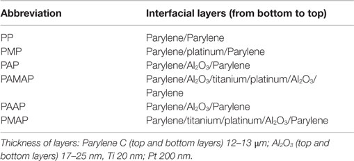
Table 2. Different material combinations investigated for flexible Parylene devices.
Peel Tests
Peel Test Device Design
Delamination is a common concern for thin-film polymeric devices, especially in aqueous solutions (Li et al., 2008b). Any interface in a thin-film polymer device that delaminates could potentially create paths to water intrusion and so determining the adhesion strength between layers is important. Thin films can bond to underlying substrates physically by filling in pores or surface topography, through covalent bonds, or by van der Waals forces. In addition, interfaces that typically have poor adhesion, such as Parylene deposited on silicone, can be improved with adhesion promoters, such as the silane A-174, which bonds covalently both with Parylene free radicals during the deposition process and provide a strong linkage with the underlying substrate (Charmet et al., 2013). Also, a combination of heat and compression can bond Parylene layers together by causing the polymer chains on the surface of the touching films to become entangled (Noha et al., 2004). Computational models suggest that metals, such as platinum and titanium can form stable and covalent bonds when deposited on Parylene (Vasenkov, 2011). Water intrusion (both from the edges of thin-film devices and through the polymer layers themselves) can weaken adhesion by penetrating between physical bonds or dissolving intermediate layers. Delamination occurs when upward forces perpendicular to the substrate are stronger than adhesion forces the top film.
Several methods have been used to measure the adhesion force of thin films. The “scotch test tape” qualitative tests the adhesion of a film deposited on a substrate by applying a piece of pressure sensitive tape to the film and pulling the tape off (Lim et al., 2006; Sridhar et al., 2009). If the top layer of the deposited film comes off (either in parts or in pieces), it is said to have “failed” the test.
The adhesion force of the film can also be determined using a load cell connected to the free end of a film which is then pulled at a 90° angle to a fixed substrate (Chang et al., 2011) or 180° to a second attached flexible film, to measure force required to separate the film from a substrate. The peel strength is defined as the average load per unit width of bondline required to progressively separate the two materials.
When the film is pulled at a 180° angle, the test is called a “T-peel test” because of the shape formed by the two free ends pulled and the bonded perpendicular region forming base of the “T” (Table 1). T-peel tests are used for the simplicity of the test setup and ability to compare different forms of bonding or adhesives (Song and Yu, 2002); however, these tests are sensitive to the thickness of the substrates, which require energy to deform during the test and must be accounted for if direct measurement of cohesion strength is desired (Kim, 1988).
In the current experiment, T-peel tests were performed with specimens based on ASTM standard D1876-08, but modified to be used on thin-film devices. These tests allowed the peel strength of multiple interfaces to be measured, including PP, PMP, PMAP, PAP, PAMAP, and PAAP (Table 2).
Peel Test Device Fabrication
In addition to the fabrication steps described in Section “Device Fabrication” (Figure S1 in Supplementary Material), two flaps (4.3 mm × 14 mm) with 3 mm holes (for gripping) were created using a sacrificial photoresist that was later removed to enable them to be separated after the device was released (Figure S2 in Supplementary Material). The flaps were used to grip while pulling apart the bonded region (4.3 mm × 3 mm) of the device. Each Parylene layer of the peel test device was 13 μm thick.
Peel Test Setup and Characterization
Peel test devices were tested by attaching one flap to a stationary clamp and the other to a 50 g load cell (Omega, Stamford, CT, USA), which was attached to a motorized stage (Z812, Thorlabs, Newton, NJ, USA) that pulled the two flaps apart at a rate of 0.02 mm/s (Figure 1). A custom Labview program was used to control the stage and measure the voltage output from the load cell (Figure 1B). PMP devices were tested both dry and after a 24-h soak in 1× PBS solution at 37°C for 24 h. Scanning electron microscope (SEM) images were taken of peel test surfaces to examine morphology of adhesion failure.
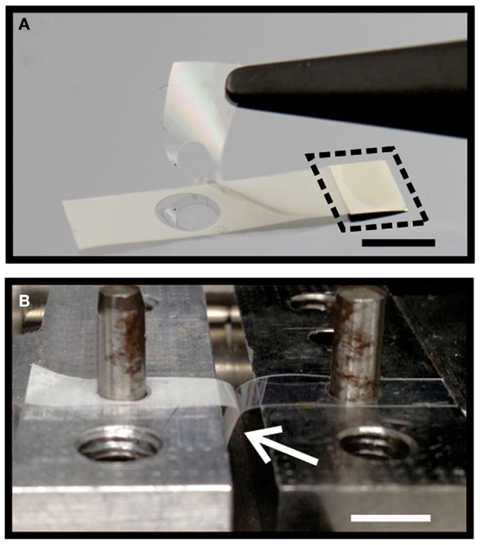
Figure 1. (A) Flaps of peel test sample separated with tweezers after removing sacrificial PR. Bonded metal region is circumscribed by dotted line. (B) Peel test sample placed over mounting posts on motorized stage with load cell before top clamp is secured. White arrow points to bonded region of peel test device [scale bars for (A) and (B) are 5 mm].
Minimum Bending Diameter Tests
Minimum Bending Diameter Device Design
Implanted thin-film polymeric devices are exposed to mechanical forces, such as muscle contractions, acceleration, gravity, hydrostatic pressure, etc., that can damage the device. Muscles can contract to 50% of their resting length (Jenkins, 2001), which can cause devices near or on their surface to be flexed, bent, or pinched. When a material is subjected to bending, it experiences compression forces on the inside surface and tensile forces on the outside surface (Figure S3 in Supplementary Material). These stresses follow a linear relationship according to the following equation for bending stress (σb):
where M is the bending moment, y is the vertical distance from the neutral axis, and I is the moment of inertia around the neutral axis. The neutral axis within the sample is where the transition from compressive to tensile forces occurs (Figure S3B in Supplementary Material). Because materials are generally fail due to cracks propagating perpendicular to tension forces, cracks in bent materials tend to propagate from the outside surface to the inside surface.
The effect of bending stress on thin-film devices can be assessed by wrapping films around cylinders of specific diameters ranging from hundreds of microns to several millimeters and then either measuring the resistance across the traces or the testing the performance (Ai et al., 2008; Chen et al., 2010; Kim et al., 2010; Lacour et al., 2010; Ochoa et al., 2013). Alternatively, films can be wrapped around spheres (Ochoa et al., 2013; Rodger et al., 2007) and inflatable balloons (Kim et al., 2011). Some devices are self-curling and were shown to maintain function while being bent 90° (Takeuchi et al., 2004) or down to a radius of 2 mm or less (Johnson and Wise, 2012; Yamagiwa et al., 2013).
A convenient and automated setup determining the minimum bend radius of a thin-film device called the “bending plate” method (Roll, 1976) involves bending a flexible film between two plates until failure (Sekitani et al., 2010). The bending plate method is a versatile technique that was developed to measure the tensile strength for optical fibers based on the distance between the plates (D) the overall fiber thickness (d), the uncoated fiber radius (r), and the Young’s modulus of the fiber (Eq. 2) (Matthewson et al., 1986), but has also been used to determine the smallest diameter that thin conductive films on flexible substrates can be bent to before registering an open circuit (Alzoubi et al., 2011; Leterrier et al., 2003) (i.e., the minimum bending diameter). The boundary condition of the bending plate method is that the radius of curvature is 0 where the plate is in contact with the cable, and the radius of curvature is maximum on the outside edge of the cable half way between the plates. The radius of curvature of the bend (R) is described by the equation: where θ is the angle formed by a line tangent to the curve of the cable and a line at the midpoint at the bend parallel with the plates, and s is the length of the line from the intersection of the line tangent to the cable with the cable to the intersection of that same line to the midline. The moments about this point are given by the bending beam equation: (Matthewson et al., 1986).
There are several advantages in using this type of bend test rather than a traditional tensile test, including eliminating the influence of the grips on the test and simple setup; however, the test is limited by difficulty in determining the exact position of 0 separation and only being able to test the portion of the sample between the plates.
To measure the minimum bending diameter of Parylene thin-film cables using this method, a thin-film flexible cable (with dimensions 48 mm × 4.3 mm × 0.026 mm) with a single 360 μm wide serpentine trace (longest straight dimension is 40 mm) was designed, whose resistance could be measured while compressing the cable between two acrylic plates (Figure 2). Failure was marked by the cable reading an open circuit. These devices were made using standard photolithographic processes described in Figure S1 in Supplementary Material.

Figure 2. (A) Cartoon and (B) photograph of minimum bending diameter test devices (scale bar is 5 mm). In cartoon (A), the thickness of the traces has been increased and number of turns decreased for illustrative purposes. The metal and hole on the left side of device are for clamping the device to the testing fixture. The contact pads on the right side allow electrical resistance measurements.
Minimum Bending Diameter Test Setup
To measure the minimum bending diameter, a thin-film cable was between two acrylic blocks while resistance was monitored (Figure S4 in Supplementary Material). One of the acrylic blocks was attached to a 50-g load cell (Omega, Stamford, CT, USA) which, in turn, was connected to a motorized stage (Z812, Thorlabs, Newton, NJ, USA) for measuring axial force for the purpose of determining complete contact between the blocks. The devices were supported by a holder and connected to a precision multimeter (Keithley 2700, Keithley, Cleveland, OH, USA). Using a custom Labview program (National Instruments, Austin, TX, USA), the motorized stage was advanced at a rate of 0.02 mm/s, bringing the two acrylic blocks together and reducing the bend diameter. Failure was defined as an open circuit measurement. The minimum diameter was measured both with the devices folded away from the contact pads (“out”) and toward the contact pads (“in”) (Figure S4 in Supplementary Material).
The acrylic blocks were visually confirmed to make full contact when the load cell read 4.5 N. To determine the minimum diameter, therefore, the position of the stage where the load cell reached 4.5 N was defined as 0, and the difference of the stage position at that point and the position of the stage where the resistance of the minimum bend diameter test device directly before the trace was measured as an open circuit was the device’s minimum diameter. The minimum bending curvature (radius) is half of the difference between the minimum bending diameter and the thickness of the thin-film device (26 μm).
To determine the failure diameter, the electrical resistance of a Pt trace across cable was monitored as a loop of cable was bent between two plates (Figure S4 in Supplementary Material).
Bending Fatigue
Bending Fatigue Device Design
When thin films are exposed to forces less than their tensile strength, even though they will not break on the first cycle, they can still fail due to fatigue caused by repeated motions present near parts of the body such as the heart, which contracts over 100k times/day, or the neck, which moves an average of 10 million times in each direction each year (Sterling et al., 2008). Fatigue occurs because dislocations and voids move and coalesce under bending stress. When a sufficient number of dislocations aggregate, crack propagation sites form that weaken the material. Fatigue in thin-film devices has been measured in test in vitro by continuously measuring resistance across polyimide (Kisban et al., 2009) or Parylene (Johnson, 2011) test cables bent to 90° angles for thousands or millions of cycles, and in vivo by measuring ECG signals for ~10,000 heart beats (Viventi et al., 2010).
To measure the effect of repeated deformation on thin-film Parylene devices, bend test samples (measuring 4.3 mm × 48 mm × 0.026 mm) with 40 mm long and 360 μm wide fully insulated traces (Figure 3) were designed and fabricated using standard lithographic techniques described in Figure S1 in Supplementary Material.
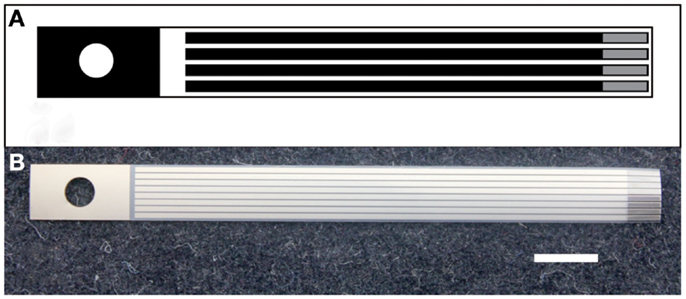
Figure 3. (A) Cartoon and (B) photograph of bend test devices (scale bar is 5 mm) [in cartoon (A), the thickness of the traces has been increased and number of traces decreased for illustrative purposes]. The metal and hole on the left side of device are for clamping the device to the testing fixture. The contact pads on the right side allow electrochemical impedance measurements with a potentiostat.
Electrochemical impedance spectroscopy (EIS) was used identify signs of failure in the device (e.g., delamination, water infiltration) by measuring the impedance between traces [the lateral impedance (Figure S5A in Supplementary Material)] and the impedance between a trace and an external counter electrode [the transverse impedance (Figure S5B in Supplementary Material)] while immersed in phosphate buffered saline (PBS).
Bending Fatigue Testing
To apply repeated bend cycles to the bending fatigue test devices, a custom cable flex tester (based on ASTM standard D4565-10 for testing cable insulation) was constructed consisting of a Sparkfun stepper motor (ROB-09238) (Sparkfun, Boulder, CO, USA) with an Arduino UNO (Arduino, Torino, Italy) controller and mounting fixtures (Figure S6 in Supplementary Material). In this setup, the top of the cable was attached to a rotating wheel and passed through two mandrels at the center of the wheel and two stationary rollers below the wheel. A weight [consisting of a section of flat flexible cable (FFC)] was attached to the bottom of the cable (below the stationary rollers) to keep the cable taut. The wheel was then rotated ±90°. As the wheel turned the cable was bent around the center mandrels, while the cable below the mandrels remained free to move up and down through the stationary rollers. For a cable bent around a mandrel, the total stress in the cable (σtotal) can be approximated as the sum of the stress due to the tensile forces (σt) caused by the weight hanging from the cable) and the bending forces (σb). Because the radius of curvature can be assumed to be the cylindrical radius of mandrel σb can be approximated as:
where E is the elastic modulus of Parylene, t is the thickness of the cable, and D is the diameter of the mandrel. In a fatigue test, σtotal is much less than the tensile stress of the cable so that multiple cycles are required before signs of fatigue become apparent. In the current test setup, devices were subject to 10–100k bending cycles in which one cycle is defined by bending the between −90° and +90° around a mandrel (1.25 mm OD).
EIS was performed in 1× PBS at 37°C with an amplitude of 10 mVrms and a frequency range of 1–100,000 Hz. A platinum wire was used as a counter electrode and an Ag/AgCl (3 M NaCl) electrode was used as a reference (transverse impedance). The impedance magnitude was normalized to absolute impedance of the magnitude at 0 bends and plotted.
In addition to EIS, devices were examined using optical and Nomarski differential interference coherence (DIC) microscopy as well as scanning electron microscopy (SEM), before and after bending.
The impedance was expected to behave according to the simplified Randle’s model, with the values for the capacitive and resistive components changing as the insulation fails [Figure S7 in Supplementary Material (Loveday et al., 2004)]. Delamination of the Parylene film is expected to cause a drop in measured impedance starting at lower frequencies, which has been shown to be more sensitive to electrode failure (Takmakov et al., 2015).
Results
Peel Testing
Peel testing resulted in characteristic T-peel curves with an increase in force once the samples become taut, and a relatively continuous force as the bonded area was separated by peeling (Figure 4). Overall, the average peel test strength of the PP devices was low with relatively large spikes observed in the force plots at the beginning and inconsistent spikes at the end of the peel tests (representative plot in Figure 4A).
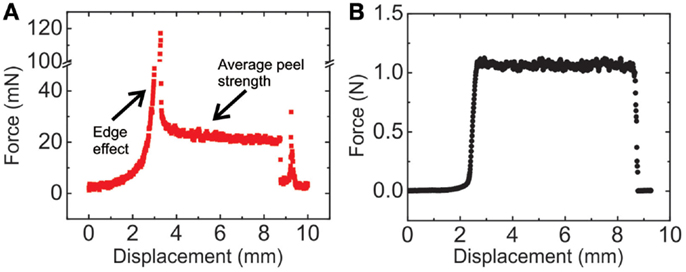
Figure 4. Representative peel test raw data from (A) PP and (B) PMP test devices. The edge effect observed for the PP device was not observed for the PMP device, most likely due to the force magnitude of being dominated by the larger PMP average peel strength (~50 times larger). Note that the two plots are on different scales.
Mean values of average peel strength are presented in Figures 5A,B indicated PMP devices, exhibited the highest adhesion (21.9 ± 1.3 N/mm, mean ± SE), followed by the PMAP, PAP, PAMAP, and PAAP devices (Figure 5A). The force required to pull apart PP and PP wet devices was the lowest (0.43 ± 0.06 and 0.21 ± 0.04 N/mm, respectively) (Figure 5B). PP samples soaked overnight at 37°C in 1 M PBS solution (PP wet) had significantly lower peel strength than devices that were not exposed to soaking (Figure 5B). In all cases, the top layer of Parylene was separated from the underlying layers.
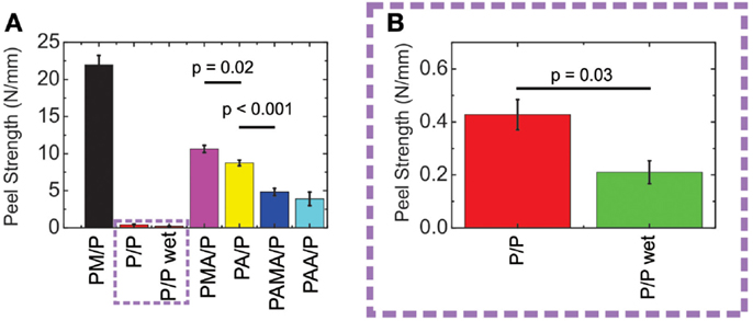
Figure 5. (A) Combined average peel test data (mean ± SE, n = 3–8) from various trials. Parylene/Parylene interfaces had the lowest peel strength and were regraphed separately (B) using a different scale. The slash indicates the interface at which delamination occurred.
Significant differences were found between PAP and PMAP and the PMAP and PAMAP devices. However, there is no significant difference between the PAMAP and PAAP devices. The cumulative mean average peel test bar graphs also show that samples with either one or two layers of Al2O3 showed much smaller variation in peel strength than samples without Al2O3 (Figure 5A).
SEM images were acquired for all conditions (Figure 6). The PMP surfaces (Figure 6A) contained cracked and delaminated Pt on the bottom layer of Parylene (left image) and plastically deformed Parylene on the top layer (right image). In contrast, the PP devices (Figure 6B) were relatively smooth and clean except for thin strands of Parylene on the bottom layer (left image). The devices with Al2O3 with or without a layer of Pt were similar (Figures 6C–F). The bottom layer of these interfaces (left images), which included the bottom layer of Parylene and one or two layers of Al2O3, contained parallel ridges topped with plastically deformed flaps of Parylene. The top layers (Figures 6C–F, right images), contained clusters of thin strings of Parylene.
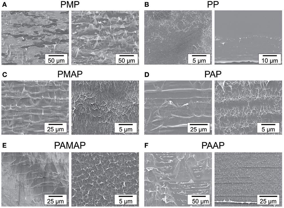
Figure 6. SEM images of peel test surfaces. For each individual panel, the left image is the bottom (closest to the silicon wafer during processing) layer (consisting of Parylene, metal, and Al2O3) and the right image is the top layer of Parylene. The PMP surface (A) contained cracked and delaminated Pt on the bottom layer of Parylene (left image) and plastically deformed Parylene on the top layer (right image). PP devices (B) were relatively smooth and clean except for thin strands of Parylene on the bottom layer (left image). Devices with Al2O3 with or without a layer of Pt (C–F) were similar in that the bottom layers (left images) contained parallel ridges topped with plastically deformed flaps of Parylene and the top layers (right images) contained clusters of thin strings of Parylene. Note that images are at different scales (surfaces were sputtered coated with Pt before imaging).
Minimum Bending Diameter
A diameter of 0 mm was defined as the point in which the force measurement on the acrylic clamping blocks was 4.5 N and all data was normalized to this setting. Full contact of acrylic blocks at 4.5 N was confirmed using video images. The resistance of the traces as the bending diameter was reduced was graphed (Figure 7) and the minimum bending diameter just prior to the formation of an open circuit was recorded (Figure 8).
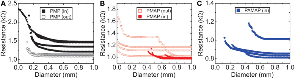
Figure 7. Resistance data from (A) PMP, (B) PMAP, and (C) PAMAP minimum bend diameter tests. Minimum bending diameter was defined as the resistance measurement closest to 0 mm not measured as an open circuit.
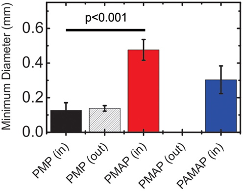
Figure 8. Summary of minimum bend test data. PMAP (in) had a significantly larger minimum bending diameter than either PMP (in) or PMP (out) (mean ± SE, n = 3–4).
The minimum bending diameter of PMP devices was measured to be 138 ± 16 μm with no significant difference between bending the device toward the top layer of Parylene (in) or toward the bottom layer of Parylene (out). Contrarily, the PMAP device with one layer of Al2O3 underneath the top layer of Parylene failed much earlier (476 ± 60 μm) than the PMP devices when bent toward the Al2O3 layer, but did not break at all when bent away from the Al2O3 layer. The low yield of PAMAP devices was attributed to difficulty in establishing electrical contact and therefore, PAMAP devices were only tested under bending toward the top layer of Parylene.
SEM images were taken of both the top and bottom surfaces of devices that had been bent away from (Figure 9) and toward (Figure 10) the contact pads. Cracks that formed due to tension on the outside of the bend (Figures 9A,C and 10A,C) appeared to be deeper with cleaner edges compared to cracks formed due to compression on the inside of the bent device (Figures 9B,D and 10B,D), which are characterized by rope-like ridges of Parylene accompanied by plastically deformed shark-tooth shaped fringes.
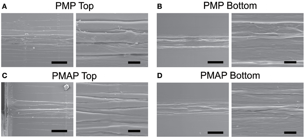
Figure 9. SEM of cracks resulting from bending (A,B) PMP devices and (C,D) PMAP devices away from the contact pads (“out” orientation). The top layers of Parylene (A,C) were the outside of the bent device, and the bottom layer (C,D) were from the inside of the bent device (images on the right side of each panel are zoomed in views of images on the left with scale bars of the left and right images being 50 and 10 μm, respectively. Parylene sputtered coated with Pt before imaging).
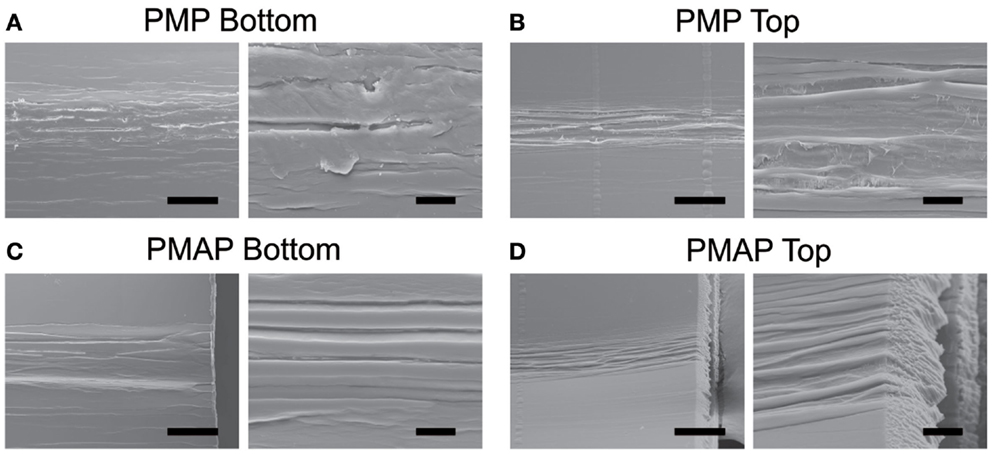
Figure 10. SEM of cracks resulting from bending (A,B) PMP devices and (C,D) PMAP devices toward the contact pads (“in” orientation). The bottom layers of Parylene (A,C) were the outside of the bent device, and the top layer (C,D) were from the inside of the bent device (images on the right side of each panel are zoomed in views of images on the left with scale bars of the left and right images being 50 and 10 μm, respectively. Parylene sputtered coated with Pt before imaging). In the PMAP sample, delamination at the bend was observed.
Bending Fatigue
EIS of a PMP device released from a wafer that showed inconsistent adhesion during peel testing (data not shown) demonstrated the ability to reveal insulation damage without destructive testing (Figure 11). The magnitude of the transverse impedance gradually decreased at lower frequencies after even only 100 bend cycles, followed by a broad spectrum decrease after 5k bend cycles (Figures 11A,B). Similarly, the phase decreased at lower frequencies during the first 4k bend cycles, and then at higher frequencies after 5k bend cycles (Figure 11C). The lateral impedance proved to be more sensitive, showing a broad spectrum decrease in the magnitude of the impedance at 4k as well as 5k (Figures 11D,E). Before bend testing (0 cycles), the lateral impedance had a −90° phase at all frequencies, which is indicative of a fully insulated trace. However, the phase dropped at lower frequencies as soon as bend testing began, and there was a broad spectrum drop after 4k cycles (Figure 11F). Broad spectrum decreases in magnitude and phase suggested that the insulation has been damaged and there was a path for ions to move between traces.
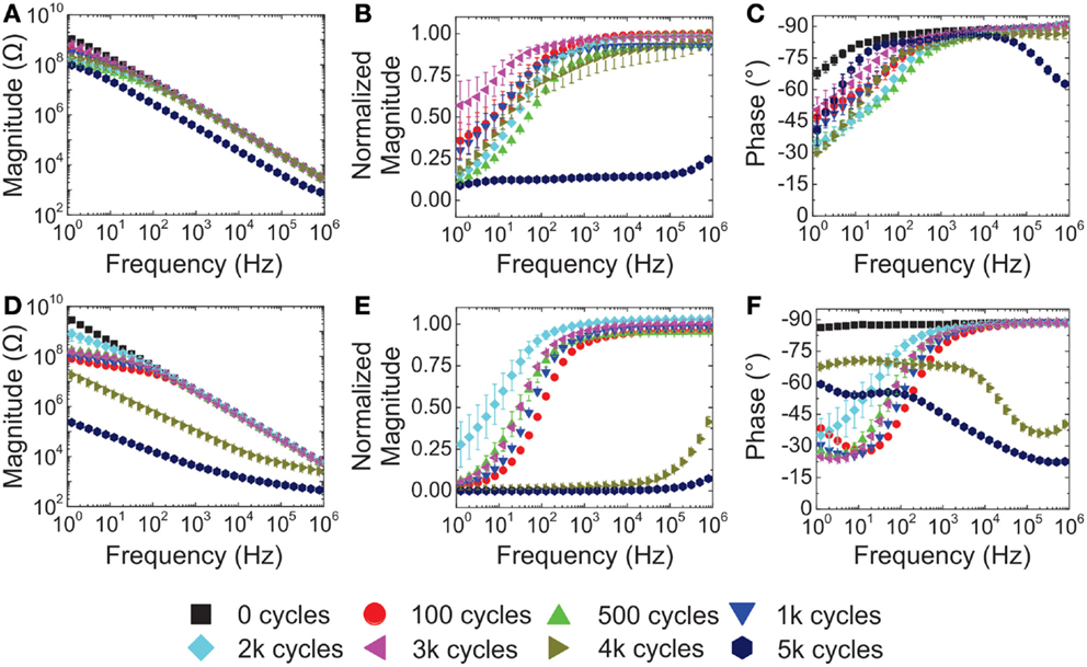
Figure 11. Representative transverse (A–C) and lateral (D–F) impedance from a PMP device released from a wafer that peel testing revealed had uneven adhesion of the top layer of Parylene. A clear change in impedance over 5k bend cycles is evident and represented by downward shifts in magnitude (A,D) emphasized by normalizing the data to the impedance magnitude at 0 bends (B,E), and shifts in phase (C,F) at high and low frequencies (mean ± SE, n = 8).
The average transverse impedance from PMP devices (which peel testing showed good adhesion between the Parylene and metal (Figure 12) showed a small drop in magnitude at lower frequencies, but remained relatively constant at higher frequencies (Figure 12A). However, as the number of bend cycles increased, the impedance at lower frequencies became lower. The phase of the PMP devices was initially −90°, but increased at lower frequencies after the first set of bends. At higher frequencies, the phase remained capacitive (around 90°) even when the devices were bent through 100k cycles (Figure 12B). In contrast to the PMP devices, the PMAP and PAMAP exhibited larger fluctuations in magnitude over most frequencies (Figures 12C,E) and compromised insulation prior to bending based on the phase data (Figures 12D,F).
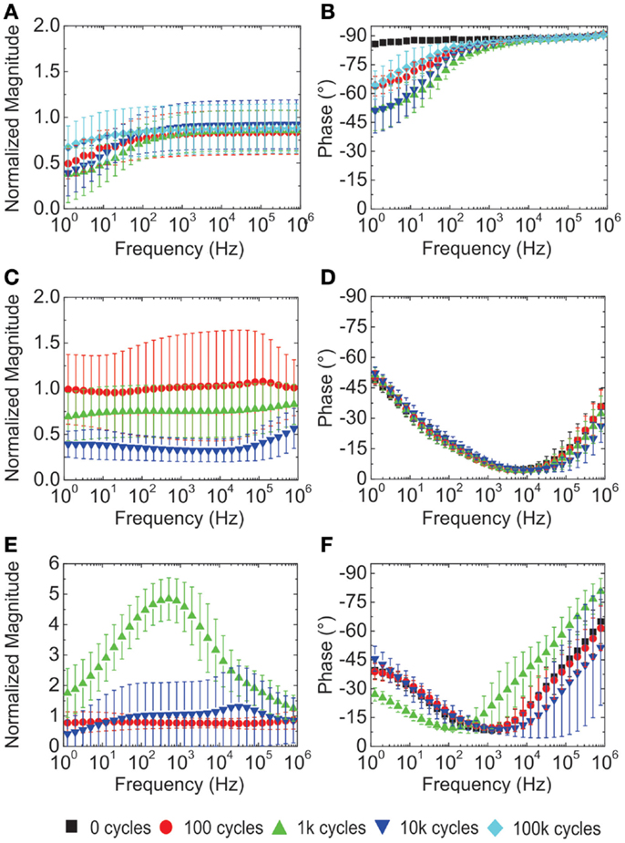
Figure 12. Transverse impedance from (A,B) PMP, (C,D) PMAP, and (E,F) PAMAP Parylene cables (mean ± SE, n = 16). Magnitude was normalized with respect to the impedance at 0 cycles (PMAP and PAMAP devices were only bent for 10k cycles).
The phase for PMP devices under lateral impedance testing started greater than −90° at lower frequencies (Figure 13B). However, similar to the transverse impedance, there was no broad spectrum shift of magnitude, but only a decrease at lower frequencies (Figure 13A). Similar to the transverse impedance, the lateral impedance of the devices with Al2O3 had large shifts in magnitude with large SEs (Figures 13C,E). In addition, the initial phase was greater than −90° even before the devices were bent (Figures 13D,F).
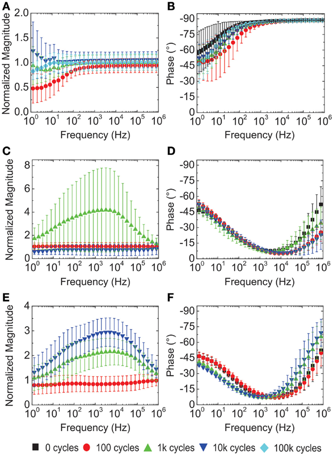
Figure 13. Lateral impedance from (A,B) PMP, (C,D) PMAP, and (E,F) PAMAP Parylene cables (mean ± SE, n = 16). Magnitude of impedance was normalized to the impedance of the device at 0 cycles (PMAP and PAMAP were only bent for 10k cycles).
Cracks in the Parylene that started at edges (not shown) were visible by optical microscopy after 2k bend cycles (Figure 14A) and became pronounced after 5k bend cycles (Figure 14B). The cracks were either chevron-like, radiating from a central point such (top left traces in Figure 14B) or perpendicular to the traces (right trace in Figure 14B). Cracks were observed to cross over the metal traces and the Parylene region between traces after 100k bend cycles (Figure S8 in Supplementary Material).
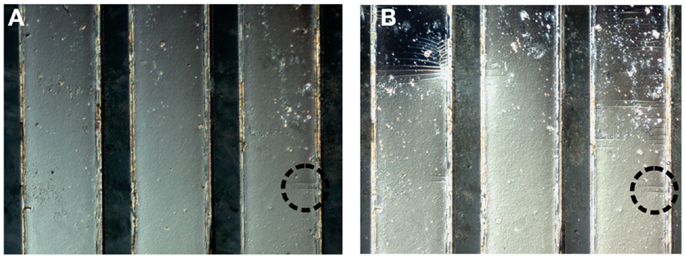
Figure 14. Nomarski differential interference contrast images of fatigue cracks in the top Parylene layer covering three traces of a PAMAP devices after (A) 2k bend cycles and (B) 5k bend cycles. Metal regions are wide, light gray strips and Parylene appears as thin, dark gray strips. The majority of cracks appeared after 5k bend cycles; however, the dashed circle marks cracks present after 2k cycles (circle is 200 μm in diameter).
Optical micrographs of PMAP and PAMAP devices showed noticeable water intrusion after 100 bend cycles (images were not taken after the initial pre-bend EIS and before first bend testing cycles) and continued to be present after subsequent bend tests (Figure S9 in Supplementary Material). In Figure S9 in Supplementary Material, Newton rings were observed in the Parylene next to the edge of the device, but there was also evidence of Newton rings near the bottom of the right trace.
Evidence of Al2O3 etching was evident in pock marks on the traces (Figure S9 in Supplementary Material) as well as discoloration and branched patterns that initiated from the outside traces (Figure 15A). The impedance of the traces measured at 1 kHz before bend testing commenced was much lower toward the edges of the device, but as the device was subjected to further bending and EIS scans (each time an EIS was performed on all traces, the devices were immersed in PBS for ~45 min), the impedance was reduced across all traces and became more uniform (Figure 15B).
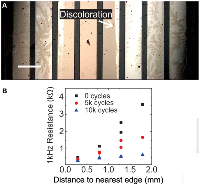
Figure 15. (A) Micrograph of all eight traces of a PMAP device showing discoloration and branched patterns occurring on outside traces (scale bar is 500 μm). (B) The transverse impedance at 1 kHz for the traces shown in (A) versus their proximity to the edge. Before bend testing, traces closest to the edge had the lowest impedance, but this difference decreased as the device was exposed to more bend cycles.
Discussion
Peel Testing
SEM images (not shown) revealed trace amounts of sacrificial photoresist that had not been fully removed from the Parylene flap regions, which may have caused the large spikes at the beginning of the PP peel tests (Figure 4A). The inconsistencies at the end of the test were mostly likely due to edge effects as the sample twisted when only a portion of the adhered regions were separated. This caused the samples to reorient so that the pulling force acted preferentially on the bonded surface area over the bondline. In contrast, the PMP interfaces were much stronger than the PP interfaces and likely dominated any edge effects (Figure 4B).
Peel tests revealed that PMP interfaces had the strongest adhesion measuring nearly 20 times more than for PP interfaces. PP interfaces were further weakened by soaking for 24 h in 1 M PBS at 37°C (Figure 5). The reduced adhesion in soaked samples is likely due to water intrusion between the layers. The Al2O3–Parylene interface was weaker than Pt–Parylene but stronger than PP. However, the adhesion between Al2O3–Parylene interfaces for different processing conditions was inconsistent. The PAMAP and PAAP devices had lower strength than the devices with only one layer of Al2O3. This is attributed to extra processing steps required for the extra layer of Al2O3. These results imply that excellent adhesion is possible between platinum and Parylene, which has been suggested through the results of modeling (Vasenkov, 2011), and that platinum could potentially be used as an adhesion promoter between Parylene layers. The higher PMAP and PAMAP peel strength compared to PP also suggested that Al2O3 and A-174 could promote adhesion between two layers of Parylene.
In all cases, the top layer of Parylene deposited on Parylene, metal, or Al2O3, always separated from the underlying layer after peel testing. This indicated that the interface between materials (metal and Al2O3) deposited onto Parylene possessed greater adhesion than the interface formed when Parylene was deposited onto the same materials. Therefore, strategies to promote adhesion should focus on the substrate-Parylene interface.
Minimum Bending Diameter
The variation in minimum bending diameter between the PMP and the PMAP devices was likely due to the adhesion strength between the two layers. Because materials are stronger in compression than compression, cracks generally initiated on the outside edge of a bent cable and then propagated toward the inner edge. However, if there was poor adhesion between the Al2O3 and top layer of Parylene, then the crack could not easily propagate between the two layers of Parylene separated by Al2O3. Conversely, it was observed that for PMAP devices oriented “in”, the metal trace is bonded to the outside layer of Parylene and cracked when the outside layer of Parylene cracks. When there was good adhesion on both sides, such as with the PMP devices, the traces lay along a neutral plane (Figure S3 in Supplementary Material), which reduced forces on the traces and resulted in breaking below the same minimum bending diameter, whether being bent “in” or “out”.
These results suggest that if it is desired to make devices with very tight diameters in one direction, it should be possible to deposit metal on only one side of a material, or make one layer of insulation thinner than the other and then fold the device toward the thinner layer of insulation. Depositing metal on only one side of the Parylene would also make the device prone to curling due to residual stresses in the various layers, which have been measured as 22 MPa (Dabral et al., 1992; Harder et al., 2002), 230 MPa (Branger et al., 1996), and 383 MPa (Tripp et al., 2006), for Parylene, platinum, and Al2O3, respectively. Curling was not observed on our devices because the sandwich structure caused the residual stress in the two layers to cancel out (Branger et al., 1996). Also, the Pt and Al2O3 layers are thin compared to Parylene and the radius of curvature is proportional to the square of the thickness of the substrate over the thickness of the film. Accordingly, after the top layer of Parylene was removed from the PMP peel test samples, the side with the metal formed tight curls as would be predicted by the Stoney equation (Eq. 4) (Ohring, 2001) where σf and hf are the internal stress and thickness of the film, Es, hs, and υs are the Young’s modulus, thickness, and the Poisson’s ratio of the substrate, and κ is the radius of curvature.
The results of the minimum bending diameter tests also suggest that improving adhesion when the metal traces lie along the neutral plane should improve bidirectional bending of devices.
Bending Fatigue
The average transverse impedance from a PMP devices (which peel testing showed good adhesion between the Parylene and metal (Figure 5) dropped slightly in magnitude at lower frequencies which are more sensitive to device failure (Fernández et al., 2014), but remained relatively constant at higher frequencies (Figure 12A). The −90° phase of the PMP devices suggested that traces were fully insulated before bending, however, the insulation was in part compromised after the first set of bend tests as indicated by the drop in phase at lower frequencies. Notably, however, the phase remained capacitive at higher frequencies even when the devices were bent through 100k cycles (Figure 12B) indicating that the insulation was at least partially intact.
In contrast to the PMP devices, the PMAP and PAMAP devices showed large variations in normalized magnitude, indicating large changes in the insulation. Increases in the magnitude (Figure 12E) could be due to cracks that broke the traces which would increase the impedance. The decrease in impedance back to the baseline after 10k bends could be due to re-established contact between broken traces, or further deterioration of the insulation through delamination. The small phase even at 0 bends (Figures 12D,F) indicates that there was an almost immediate intrusion of ions across the insulation to the traces in those devices. The large SE in the magnitude and phase of the PAMAP devices (Figures 12C,E) pointed to a wide variation in trace performance, which could be caused by flaws introduced during processing Al2O3 (addressed in the next section) or water intrusion.
The phase of the lateral impedance of the PMP devices was greater than −90° at lower frequencies before the devices were bent indicating that there were ionic paths between traces that could not be detected when measuring transverse impedance (Figure 13B). However, similar to the transverse impedance, the absence of a broad spectrum decrease in magnitude and the presence of an enduring capacitive phase (−90°) at higher frequencies implied that at least part of the Parylene insulation remained intact up to 100k bend cycles. Also similar to the transverse impedance, the phase of the lateral impedance of Al2O3 devices had small phase shifts, which suggested open ion paths between traces (Figures 13C–F).
Fatigue cracks in the Parylene were visible in the cables after 2k bends (Figure 14A). The number and size of the cracks increased with more bends (Figure 14B). The cracks appeared to originate in the Parylene layer and not the metal as the first appearance was on the device edges (in which there was no metal) and the cracks spanned across areas with and without metal (Figures S8A,B in Supplementary Material). In addition, while all devices showed extensive cracking, PMP devices did not exhibit impedance changes. Cracking in Parylene can also occur due to excessive heat (Hsu et al., 2007; Li et al., 2010), when flexed during accelerated lifetime testing (Minnikanti et al., 2013), and in long-term in vivo testing (Schmidt et al., 1988).
Failure of Al2O3 Devices
Optical micrographs of PMAP and PAMAP devices showed noticeable water intrusion after 100 bend cycles (images were not taken before 100 bend cycles) (Figure S9 in Supplementary Material). Water intrusion was more pronounced on Al2O3 devices and could be attributed to the reduced hydrophobicity of Al2O3 compared to Parylene and the removal of Al2O3 upon exposure to water by etching (Abdulagatov et al., 2011). Based on the impedance measurements, the water intrusion related etching of Al2O3 started on the device edges and propagated inward toward the center. These results indicate the open edges on the sides of Parylene thin-film devices [Figure S1 in Supplementary Material (steps 5 and v)] allowed Al2O3 to be etched by the surrounding water. Assuming that Parylene films can sufficiently prevent water condensation, Al2O3 should be completely encapsulated in Parylene for devices intended for use in wet applications including implantation.
Conclusion
Thin-film flexible electronics have great potential as implantable devices. Many different thin-film devices have been demonstrated to be used to stimulate and record from many electrically active tissues such as the spinal cord (Rodger et al., 2007), heart (Viventi et al., 2010; Zhao et al., 2013), muscle (Spence et al., 2007), and cortex (Kim et al., 2013; Tolstosheeva et al., 2011). Although these studies have demonstrated the performance of the devices for short periods of time for their given application, there have not been comprehensive methods to test the mechanical properties of such thin-film architectures until failure. In this paper, simple devices and testing methods were presented to test the mechanical properties of thin-film architectures. In particular methods for measuring the peel strength, minimum bending diameter and bending fatigue failure were presented. These methods were then applied to a Parylene–metal–Parylene system with and without an Al2O3 layer, which others have used as a water barrier.
Peel tests showed that Al2O3 and A-174 can be used to increase the adhesion between two Parylene films, but that adhesion force is less than for Parylene–platinum interfaces. Parylene films deposited onto surfaces did not adhere as well as platinum and Al2O3 deposited onto Parylene. Minimum bend diameter tests showed that adding Al2O3 underneath the top Parylene allows the devices to be bent into tighter diameters when bent away from the Al2O3, but increased the minimum bending diameter when bent toward the Al2O3, likely due to poor adhesion. EIS performed on devices undergoing fatigue tests, showed that PMP can withstand up to 100k bends without significant evidence of insulation failure. When exposed to water, devices having Al2O3 failed earlier due to the etching of the film exposed at device boundaries.
Conflict of Interest Statement
The authors declare that the research was conducted in the absence of any commercial or financial relationships that could be construed as a potential conflict of interest.
Acknowledgments
This work was funded by the NSF under award number EFRI-1332394. The authors thank Dr. Donghai Zhu of the Keck Photonics laboratory for help with fabrication, Jon Curulli of the Center for Electron Microscopy and Microanalysis for help with SEM images, Dr. J. Provine of Stanford University for applying the Al2O3 coatings and members of the Biomedical Microsystems laboratory of USC for their assistance.
Supplementary Material
The Supplementary Material for this article can be found online at http://journal.frontiersin.org/article/10.3389/fmech.2015.00010
References
Abdulagatov, A., Yan, Y., Cooper, J., Zhang, Y., Gibbs, Z., Cavanagh, A., et al. (2011). Al2O3 and TiO2 atomic layer deposition on copper for water corrosion resistance. ACS Appl. Mater. Interfaces 3, 4593–4601. doi: 10.1021/am2009579
Ai, L., Yu, H., Rouhanizadeh, M., Takabe, W., Meng, E., Kim, E., et al. (2008). “Polymer-based sensors for dynamic intravascular shear stress analysis,” in ASME 2008 3rd Frontiers in Biomedical Devices Conference, Irvine, CA.
Alzoubi, K., Hamasha, M. M., Lu, S., and Sammakia, B. (2011). Bending fatigue study of sputtered ITO on flexible substrate. J. Disp. Technol. 7, 593–600. doi:10.1109/JDT.2011.2151830
Branger, V., Pelosin, V., Badawi, K., and Goudeau, P. (1996). Study of the mechanical and microstructural state of platinum thin films. Thin Solid Films 275, 22–24. doi:10.1016/0040-6090(95)07011-7
Chang, J., Lu, B., and Tai, Y.-C. (2011). “Adhesion-enhancing surface treatments for parylene deposition,” in 16th International Solid-State Sensors, Actuators and Microsystems Conference (TRANSDUCERS), Beijing, China.
Charmet, J., Bitterli, J., Sereda, O., Liley, M., Renaud, P., and Keppner, H. (2013). Optimizing parylene C adhesion for MEMS processes: potassium hydroxide wet etching. J. Microelectromech. Syst. 22, 855–864. doi:10.1109/JMEMS.2013.2248126
Chen, P.-J., Saati, S., Varma, R., Humayun, M. S., and Tai, Y.-C. (2010). Wireless intraocular pressure sensing using microfabricated minimally invasive flexible-coiled LC sensor implant. J. Microelectromech. Syst. 19, 721–734. doi:10.1109/JMEMS.2010.2049825
Dabral, S., Van Etten, J., Zhang, X., Apblett, C., Yang, G.-R., Ficalora, P., et al. (1992). Stress in thermally annealed parylene films. J. Electron. Mater. 21, 989–994. doi:10.1007/BF02684208
Fernández, E., Greger, B., House, P. A., Aranda, I., Botella, C., Albisua, J., et al. (2014). Acute human brain responses to intracortical microelectrode arrays: challenges and future prospects. Front. Neuroeng. 7:24. doi:10.3389/fneng.2014.00024
Fonseca, M. A., Allen, M. G., Kroh, J., and White, J. (2006). “Flexible wireless passive pressure sensors for biomedical applications,” in Tech. Dig. Solid-State Sensor, Actuator, and Microsystems Workshop (Hilton Head, SC).
Ghosh, A., Gerenser, L., Jarman, C., and Fornalik, J. (2005). Thin-film encapsulation of organic light-emitting devices. Appl. Phys. Lett. 86, 223503. doi:10.1063/1.1929867
Gray, D. S., Tien, J., and Chen, C. S. (2004). High-conductivity elastomeric electronics. Adv. Mater. Weinheim 16, 393–397. doi:10.1002/adma.200306107
Guo, L., Ma, M., Zhang, N., Langer, R., and Anderson, D. G. (2014). Stretchable polymeric multielectrode array for conformal neural interfacing. Adv. Mater. Weinheim 26, 1427–1433. doi:10.1002/adma.201304140
Gutierrez, C., McCarty, C., Kim, B., Pahwa, M., and Meng, E. (2010). “An implantable all-parylene liquid-impedance based MEMS force sensor,” in IEEE 23rd International Micro Electro Mechanical Systems (MEMS), Hong Kong, China.
Harder, T. A., Yao, T.-J., He, Q., Shih, C.-Y., and Tai, Y.-C. (2002). “Residual stress in thin-film parylene-C,” in IEEE 15th International Micro Electro Mechanical Systems (MEMS), Las Vegas, NV.
Hsu, J.-M., Kammer, S., Jung, E., Rieth, L., Normann, R. A., and Solzbacher, F. (2007). “Characterization of parylene-C film as an encapsulation material for neural interface devices,” in presented at the 3rd Annu. Conf. Multi-Material Micro Manufacture, Borovets, Bulgaria.
Johnson, A. C. (2011). An Active Thin-Film Cochlear Electrode Array with Monolithic Backing and Curl. Doctor of Philosophy Dissertation, Electrical Engineering, University of Michigan, Ann Arbor, MI.
Johnson, A. C., and Wise, K. D. (2010). “A robust batch-fabricated high-density cochlear electrode array,” in 2010 IEEE 23rd International Conference on Micro Electro Mechanical Systems (MEMS), Hong Kong, China.
Johnson, A. C., and Wise, K. D. (2012). “A self-curling monolithically-backed active high-density cochlear electrode array,” in IEEE 25th International Conference on 25th International Conference on Micro Electro Mechanical Systems (MEMS), Paris, France.
Kim, B., Kuo, J., Hara, S., Lee, C., Yu, L., Gutierrez, C., et al. (2013). 3D Parylene sheath neural probe for chronic recordings. J. Neural Eng. 10, 045002. doi:10.1088/1741-2560/10/4/045002
Kim, D.-H., Lu, N., Ghaffari, R., Kim, Y.-S., Lee, S. P., Xu, L., et al. (2011). Materials for multifunctional balloon catheters with capabilities in cardiac electrophysiological mapping and ablation therapy. Nat. Mater. 10, 316–323. doi:10.1038/nmat2971
Kim, D.-H., Viventi, J., Amsden, J. J., Xiao, J., Vigeland, L., Kim, Y.-S., et al. (2010). Dissolvable films of silk fibroin for ultrathin conformal bio-integrated electronics. Nat. Mater. 9, 511–517. doi:10.1038/nmat2745
Kim, H., and Najafi, K. (2005). Characterization of low-temperature wafer bonding using thin-film parylene. J. Microelectromech. Syst. 14, 1347–1355. doi:10.1109/JMEMS.2005.859102
Kim, K. (1988). “Mechanics of the peel test for thin film adhesion,” in MRS Proceedings, Boston, MA.
Kisban, S., Moser, D., Rubehn, B., Stieglitz, T., Paul, O., and Ruther, P. (2009). “Fatigue testing of polyimide-based micro implants,” in 4th European Conference of the International Federation for Medical and Biological Engineering, Antwerp, Belgium.
Kuo, J. T., Kim, B. J., Hara, S. A., Lee, C. D., Gutierrez, C. A., Hoang, T. Q., et al. (2013). Novel flexible parylene neural probe with 3D sheath structure for enhancing tissue integration. Lab. Chip 13, 554–561. doi:10.1039/c2lc40935f
Lacour, S. P., Benmerah, S., Tarte, E., FitzGerald, J., Serra, J., McMahon, S., et al. (2010). Flexible and stretchable micro-electrodes for in vitro and in vivo neural interfaces. Med. Biol. Eng. Comput. 48, 945–954. doi:10.1007/s11517-010-0644-8
Leterrier, Y., Fischer, C., Médico, L., Demarco, F., Månson, J.-A. E., Bouten, P., et al. (2003). “Mechanical properties of transparent functional thin films for flexible displays,” in 46 Annual Conference of the Society of Vacuum Coaters, San Francisco.
Li, C., Wu, P.-M., Han, J., and Ahn, C. H. (2008a). A flexible polymer tube lab-chip integrated with microsensors for smart microcatheter. Biomed. Microdevices 10, 671–679. doi:10.1007/s10544-008-9178-3
Li, W., Rodger, D., Menon, P., and Tai, Y.-C. (2008b). Corrosion behavior of parylene-metal-parylene thin films in saline. ECS Trans. 11, 1–6. doi:10.1149/1.2897437
Li, W., Rodger, D. C., Meng, E., Weiland, J. D., Humayun, M. S., and Tai, Y.-C. (2010). Wafer-level parylene packaging with integrated RF electronics for wireless retinal prostheses. J. Microelectromech. Syst. 19, 735–742. doi:10.1109/JMEMS.2010.2049985
Lim, K. S., Chang, W.-J., Koo, Y.-M., and Bashir, R. (2006). Reliable fabrication method of transferable micron scale metal pattern for poly (dimethylsiloxane) metallization. Lab. Chip 6, 578–580. doi:10.1039/b514755g
Loveday, D., Peterson, P., and Rodgers, B. (2004). Evaluation of organic coatings with electrochemical impedance spectroscopy. JCT Coat. Tech. 8, 46–52.
Matthewson, M., Kurkjian, C. R., and Gulati, S. T. (1986). Strength measurement of optical fibers by bending. J. Am. Ceram. Soc. 69, 815–821. doi:10.1111/j.1151-2916.1986.tb07366.x
Metallo, C., White, R. D., and Trimmer, B. A. (2011). Flexible parylene-based microelectrode arrays for high resolution EMG recordings in freely moving small animals. J. Neurosci. Methods 195, 176–184. doi:10.1016/j.jneumeth.2010.12.005
Minnikanti, S., Pancrazio, J. J., Frewin, C. L., and Saddow, S. E. (2013). “Accelerated aging and electrochemical characterization of parylene C coated implantable microwires,” in EMBS Conference on Neural Engineering, San Diego, CA.
Noha, H.-S., Huangb, Y., and Hesketha, P. J. (2004). Parylene micromolding, a rapid and low-cost fabrication method for parylene microchannel. Sens. Actuators B Chem. 102, 78–85. doi:10.1016/S0925-4005(04)00476-9
Nomura, K., Ohta, H., Takagi, A., Kamiya, T., Hirano, M., and Hosono, H. (2004). Room-temperature fabrication of transparent flexible thin-film transistors using amorphous oxide semiconductors. Nature 432, 488–492. doi:10.1038/nature03090
Ochoa, M., Wei, P., Wolley, A. J., Otto, K. J., and Ziaie, B. (2013). A hybrid PDMS-parylene subdural multi-electrode array. Biomed. Microdevices 15, 437–443. doi:10.1007/s10544-013-9743-2
Rodger, D., Fong, A., Li, W., Ameri, H., Lavrov, I., Zhong, H., et al. (2007). “High-density flexible parylene-based multielectrode arrays for retinal and spinal cord stimulation,” in Solid-State Sensors, Actuators and Microsystems Conference (TRANSDUCERS), Lyon, France.
Roll, K. (1976). Analysis of stress and strain distribution in thin films and substrates. J. Appl. Phys. 47, 3224–3229. doi:10.1063/1.323119
Schmidt, E., McIntosh, J., and Bak, M. (1988). Long-term implants of parylene-C coated microelectrodes. Med. Biol. Eng. Comput. 26, 96–101. doi:10.1007/BF02441836
Schuettler, M., Stiess, S., King, B., and Suaning, G. (2005). Fabrication of implantable microelectrode arrays by laser cutting of silicone rubber and platinum foil. J. Neural Eng. 2, S121. doi:10.1088/1741-2560/2/1/013
Sekitani, T., Zschieschang, U., Klauk, H., and Someya, T. (2010). Flexible organic transistors and circuits with extreme bending stability. Nat. Mater. 9, 1015–1022. doi:10.1038/nmat2896
Seymour, J. P., Elkasabi, Y. M., Chen, H.-Y., Lahann, J., and Kipke, D. R. (2009). The insulation performance of reactive parylene films in implantable electronic devices. Biomaterials 30, 6158–6167. doi:10.1016/j.biomaterials.2009.07.061
Song, J., and Yu, J. (2002). Analysis of the T-peel strength in a Cu/Cr/polyimide system. Acta Mater. 50, 3985–3994. doi:10.1016/S1359-6454(02)00197-0
Spence, A. J., Neeves, K. B., Murphy, D., Sponberg, S., Land, B. R., Hoy, R. R., et al. (2007). Flexible multielectrodes can resolve multiple muscles in an insect appendage. J. Neurosci. Methods 159, 116–124. doi:10.1016/j.jneumeth.2006.07.002
Sridhar, A., Van Dijk, D., and Akkerman, R. (2009). Inkjet printing and adhesion characterisation of conductive tracks on a commercial printed circuit board material. Thin Solid Films 517, 4633–4637. doi:10.1016/j.tsf.2009.03.133
Sterling, A. C., Cobian, D. G., Anderson, P. A., and Heiderscheit, B. C. (2008). Annual frequency and magnitude of neck motion in healthy individuals. Spine 33, 1882–1888. doi:10.1097/BRS.0b013e31817e7019
Takeuchi, S., Suzuki, T., Mabuchi, K., and Fujita, H. (2004). 3D flexible multichannel neural probe array. J. Micromech. Microeng. 14, 104. doi:10.1088/0960-1317/14/1/014
Takmakov, P., Ruda, K., Phillips, K. S., Isayeva, I. S., Krauthamer, V., and Welle, C. G. (2015). Rapid evaluation of the durability of cortical neural implants using accelerated aging with reactive oxygen species. J. Neural Eng. 12, 026003. doi:10.1088/1741-2560/12/2/026003
Toda, H., Suzuki, T., Sawahata, H., Majima, K., Kamitani, Y., and Hasegawa, I. (2011). Simultaneous recording of ECoG and intracortical neuronal activity using a flexible multichannel electrode-mesh in visual cortex. Neuroimage 54, 203–212. doi:10.1016/j.neuroimage.2010.08.003
Tolstosheeva, E., Gordillo-González, V., Hertzberg, T., Kempen, L., Michels, I., Kreiter, A., et al. (2011). “A novel flex-rigid and soft-release ECoG array,” in Annual International Conference of the IEEE Engineering in Medicine and Biology Society (EMBC), Boston, MA.
Tripp, M. K., Stampfer, C., Miller, D. C., Helbling, T., Herrmann, C. F., Hierold, C., et al. (2006). The mechanical properties of atomic layer deposited alumina for use in micro-and nano-electromechanical systems. Sens. Actuators A Phys. 130, 419–429. doi:10.1016/j.sna.2006.01.029
Vanhoestenberghe, A., and Donaldson, N. (2013). Corrosion of silicon integrated circuits and lifetime predictions in implantable electronic devices. J. Neural Eng. 10, 031002. doi:10.1088/1741-2560/10/3/031002
Vasenkov, A. V. (2011). Atomistic modeling of parylene-metal interactions for surface micro-structuring. J. Mol. Model. 17, 3219–3228. doi:10.1007/s00894-011-0996-5
Viventi, J., Kim, D.-H., Moss, J. D., Kim, Y.-S., Blanco, J. A., Annetta, N., et al. (2010). A conformal, bio-interfaced class of silicon electronics for mapping cardiac electrophysiology. Sci. Transl. Med. 2, 24ra22. doi:10.1126/scitranslmed.3000738
Xie, X., Rieth, L., Caldwell, R., Diwekar, M., Tathireddy, P., Sharma, R., et al. (2013). Long-term Bi-layer encapsulation performance of atomic layer deposited Al2O3 and parylene C for biomedical implantable devices. J. Neural Eng. 60, 2943–2951. doi:10.1109/TBME.2013.2266542
Xie, X., Rieth, L., Merugu, S., Tathireddy, P., and Solzbacher, F. (2012). Plasma-assisted atomic layer deposition of Al2O3 and parylene C bi-layer encapsulation for chronic implantable electronics. Appl. Phys. Lett. 101, 093702. doi:10.1063/1.4748322
Yamagiwa, S., Ishida, M., and Kawano, T. (2013). “Self-curling and-sticking flexible substrate for ECoG electrode array,” in IEEE 26th International Conference on Micro Electro Mechanical Systems (MEMS), Taipei, Taiwan.
Yu, F., Zhao, Y., Gu, J., Quigley, K. L., Chi, N. C., Tai, Y.-C., et al. (2012). Flexible microelectrode arrays to interface epicardial electrical signals with intracardial calcium transients in zebrafish hearts. Biomed. Microdevices 14, 357–366. doi:10.1007/s10544-011-9612-9
Zhao, Y., Yu, F., Cao, H., Chang, H., Zhang, X., Hsiai, T. K., et al. (2013). “A wearable percutaneous implant for long term zebrafish epicardial ECG recording,” in The 17th International Conference on Solid-State Sensors, Actuators and Microsystems (TRANSDUCERS & EUROSENSORS XXVII), Barcelona, Spain.
Keywords: Parylene, thin-film polymer, peel test, bend test, fatigue test, EIS, Al2O3
Citation: Lee CD and Meng E (2015) Mechanical properties of thin-film Parylene–metal–Parylene devices. Front. Mech. Eng. 1:10. doi: 10.3389/fmech.2015.00010
Received: 01 July 2015; Accepted: 18 August 2015;
Published: 08 September 2015
Edited by:
Weileun Fang, National Tsing Hua University, TaiwanCopyright: © 2015 Lee and Meng. This is an open-access article distributed under the terms of the Creative Commons Attribution License (CC BY). The use, distribution or reproduction in other forums is permitted, provided the original author(s) or licensor are credited and that the original publication in this journal is cited, in accordance with accepted academic practice. No use, distribution or reproduction is permitted which does not comply with these terms.
*Correspondence: Ellis Meng, Biomedical Microsystems Laboratory, Department of Biomedical Engineering, 1042 Downey Way, DRB-140, Los Angeles, CA 90089-1111, USA,ZWxsaXMubWVuZ0B1c2MuZWR1