 Luis Guillermo Villanueva
 Joan Bausells
 Juergen Brugger
- 1Ecole Polytechnique Fédérale de Lausanne, Lausanne, Switzerland
- 2Institute of Microelectronics of Barcelona, National Microelectronics Centre-CSIC, Barcelona, Spain
Micro-Electro-Mechanical-Systems
Micro-electro-mechanical-systems (MEMS) have seen a very steep progression in R&D in the 1980s and 1990s, both in academia and industry. The rapid growth has been enabled by new fabrication methods derived from semiconductor integrated circuit manufacturing. These are basically lithography, thin film deposition dry and wet etching, which were tailored for MEMS purposes, since MEMS often uses silicon not only as semiconducting but also primarily as mechanical material (Petersen, 1982). Today, some MEMS-based products are a mature industry that delivers commodity products for our everyday life, such as integrated multi sensor modules (9 degrees-of-freedom inertial, gas, pressure, temperature, and flow), actuators (inkjet nozzles, digital mirror displays), communication components (RF filters, oscillators, duplexers), and other transducers (power harvesters). The forecasts for the MEMS market show a compound annual growth rate of 5–24% for the period 2013–2019 (Yole Développement, 2015). The increasing impact that MEMS are having on markets is caused by their typically small size, which makes them minimally invasive into larger systems (cars, domotic, health care), and cost-efficient to produce, therefore facilitating their implementation in portable, ubiquitous electronics. Figure 1 shows some representative examples of advanced MEMS. However, according to the International Technology Roadmap for Semiconductors (ITRS; 2013b) current MEMS technologies will not be able to meet next decade’s society requirements in terms of performance, functionalities, power consumption, cost, and size. Why is that? It is generally accepted that for a continuous growth, MEMS faces the following challenges.
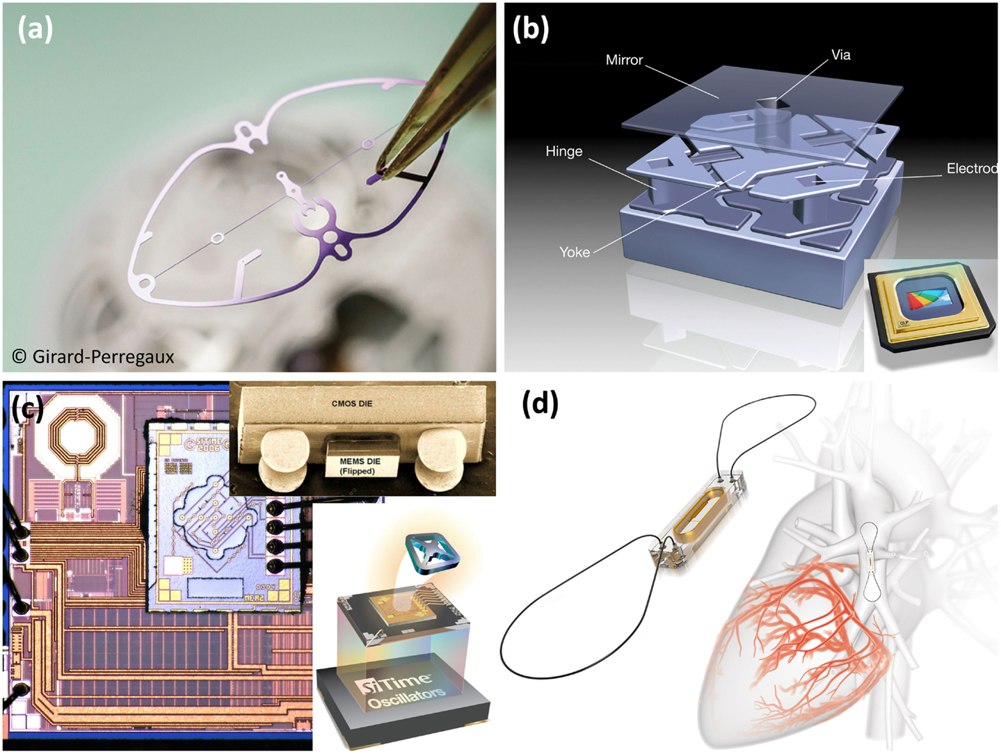
Figure 1. Commercial MEMS products. (A) Piece of a Swiss mechanical clock escapement fabricated in crystalline Si at CSEM Neuchatel, Switzerland. The high precision in manufacturing of this “macro-MEMS” implies much higher reproducibility and minimization of energy loss. Image courtesy of CSEM. (B) Schematic of a Texas Instruments (TI) Digital Light Processor (DLP) that has been powering since 1996 the world’s top display devices to deliver high-resolution images. Every DLP chipset (see inset on the bottom-right corner) features an array of microscopic mirrors that switch on and off up to 10,000 times per second. Image courtesy of TI. (C) Main - Optical microscope image of a SiTime MEMS-based oscillator, which includes a CMOS chip with the feedback circuitry and a separate chip on top with the self-packaged resonator. These oscillators are used as time references and frequency sources, and in some applications where miniaturization is paramount they have started replacing the more conventional quartz-based oscillators. Inset top-right – SEM micrograph of a newer generation where the MEMS is flip-chip bonded on the CMOS die, which is in turn ready to be flip-chip bonded on the PCB. Inset bottom-right – Cartoon showing the three levels of packaging of the SiTime oscillators – SMD level, two chips assembly, and mechanical device. Image courtesy of SiTime. (D) CardioMEMS HF System from St. Jude Medical (SJM). The system consists of a small pressure sensor (left) that can be implanted in the pulmonary artery (right) and it is powered externally via a RF signal. The sensor monitors the internal pressure in the pulmonary artery, which has been correlated to heart failure, therefore representing a major step in personalized medicine. Image courtesy of St. Jude Medical.
Scaling of MEMS
In the same way as the progression of microelectronics has been driven by Moore’s Law, which is finally motivated by economic considerations, a similar trend towards miniaturization and cost reduction is found for MEMS and its evolution toward NanoElectroMechanical Systems (NEMS). NEMS is an extension of MEMS, and throughout this article we will call them N/MEMS. They have their greatest potential in high-performance transducer applications. Indeed, N/MEMS have shown unprecedented sensing capabilities, e.g., mass (Chaste et al., 2012), force (Moser et al., 2013), surface stress (Fritz et al., 2000), or temperature (Fon et al., 2005), which has enabled the detection of tiny concentrations of gas (Li et al., 2010), single atom landing (Jensen et al., 2008), molecule surface diffusion (Yang et al., 2011), cellular stiffness (Cross et al., 2008), DNA hybridization and strand separation (Fritz et al., 2000), etc. One of the major challenges to further implementation of N/MEMS into mainstream applications is to stabilize and ultimately standardize their fabrication techniques. This would offer reproducibility, high yield and reduced cost for commodity products based on N/MEMS. On the other hand, the precision at which today materials can be shaped by micro- and nano-fabrication methods, allows also designing and building new mechanical components at the millimeter scale with extreme precision for improved performances. An example of such so-called macro-MEMS is the single-crystal silicon part of a mechanical watch.
N/MEMS, CMOS, and Post-CMOS Compatibility
One of the key points for the market penetration of N/MEMS is their compatibility with scalable wafer-based micro-fabrication techniques, paramount for the reduction in size and cost that has been attained in the past. In addition, they can be integrated with electronic circuitry, e.g., CMOS. Currently, this integration is often done in a hybrid way, i.e., the N/MEMS is fabricated on a different substrate than the electronic circuitry and then both chips are bonded together creating a system in package (SIP). This is done because current options to monolithically integrate N/MEMS and CMOS have much higher cost, mostly due to post-processing of the CMOS wafers (Villanueva et al., 2006; Arcamone et al., 2008). Size and cost will be enormously decreased if monolithic integration without post-processing would be possible. CMOS technology has been the standard for integrated circuits fabrication for over half a century. However, it is expected that within the next two decades CMOS technology will reach its scaling limits, thus requiring another technological platform to take over as the “gold standard” for nanofabrication (International Technology Roadmap for Semiconductors, 2013a). Solving the problem of co-integrating circuits and N/MEMS in such a post-CMOS scenario, where GaN and 2D materials (Banerjee and Ionescu, 2004) are two of the most promising alternatives, is a fantastic challenge for our community.
Novel N/MEMS Materials
Silicon has longtime been the standard material for MEMS, and it still is in many cases. Yet, scientific research for silicon-based MEMS has stalled in the last decade as the field came to maturation and due to successful commercialization of the above mentioned applications. The field of MEMS and NEMS, however, is much more than based solely on silicon and related materials. Advances in the science and engineering of new functional materials, including nanomaterials, and new processing methods, now allow designing and manufacturing totally new N/MEMS that will increasingly match the needs for future products (Lee et al., 2009; Ingrosso et al., 2011; Martin-Olmos et al., 2012; Jacot-Descombes et al., 2013). Some representative examples are shown in Figure 2. If one considers as a reference snapshot the N/MEMS topics covered in scientific journals in the past decade and current R&D priorities, one can see a clear trend away from physical sensors and actuators using primarily silicon as material (1980s and 1990s) toward BioMEMS, lab-on-chip and medical devices using more and more plastic and glass in the last 10 years. This tendency to integrate solid-state devices from the silicon family with polymers, biocompatible, and eventually biodegradable materials for MEMS for life-science applications represent another challenge, both at the level of integration and material development.
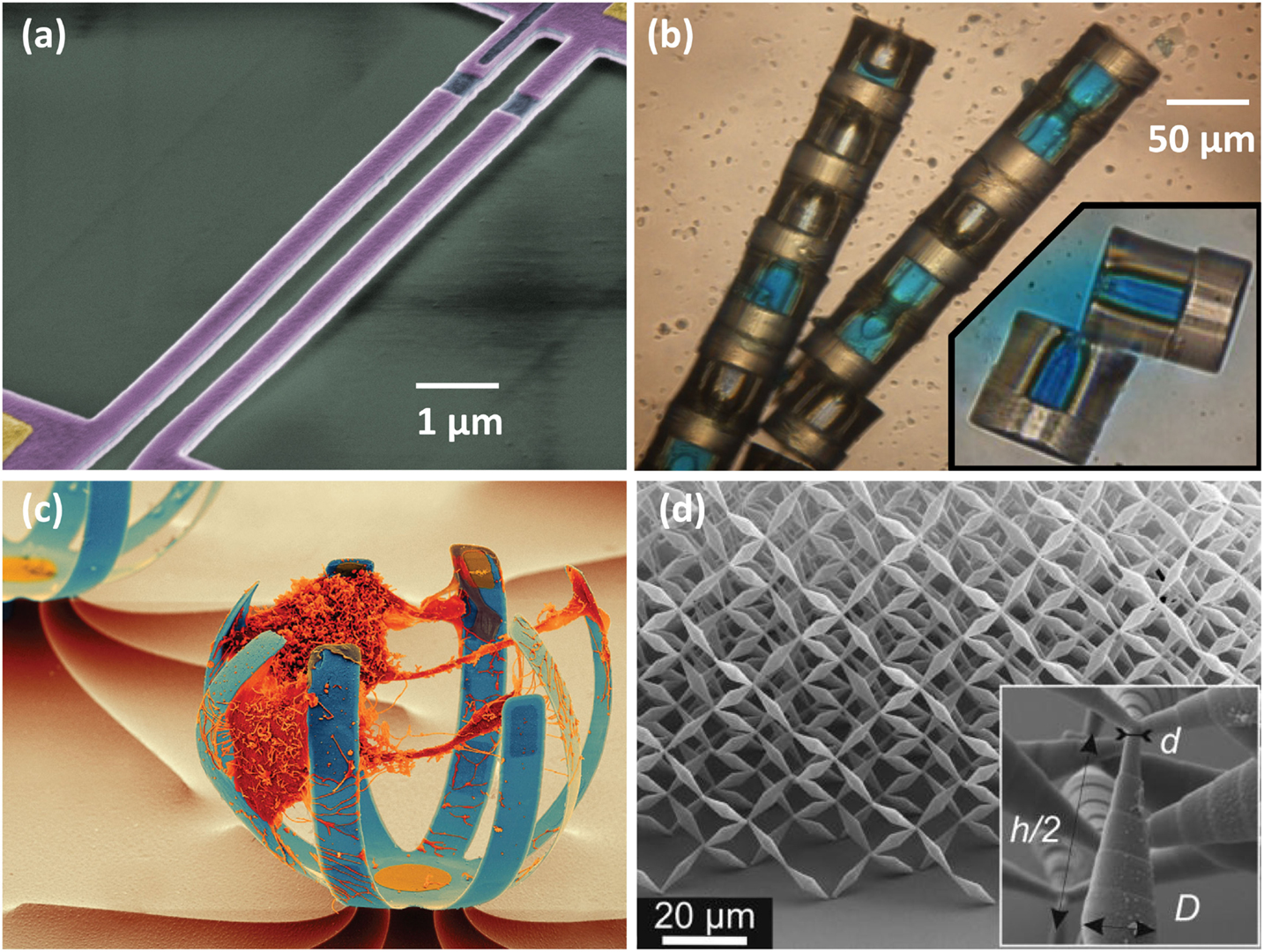
Figure 2. State of the art for micro- and nano-mechanical devices in research. (A) Scanning electron microscope (SEM) micrograph of two NEMS clamped-clamped beams. The beams are mechanically coupled through the ledge present in the anchoring region and they are fabricated using a combination of metal and piezoelectric layers, which provide the devices with self-sensing and actuating capabilities. These devices are used as coupled resonators to study complex dynamics in the nanoscale (Villanueva et al., 2011, 2013) and they also have potential for noise reduction in communications (Kenig et al., 2012) and sensitivity increase for sensing (Spletzer et al., 2006). Color has been artificially added for illustration purposes. (B) Optical microscope picture of an assembly in liquid medium of hollow half-cylinders fabricated in SU-8. Fluidic self-assembly is one of the promising novel ways that can be used to assembly MEMS/NEMS devices in large scale (Goldowsky et al., 2013; Jacot-Descombes et al., 2013). The coupled cylinders shown in the figure could be used, for example, as microcapsules for drug storage and subsequent local drug release. (C) SEM micrograph of sets of metallic cantilevers with an engineered intrinsic stress gradient in order to obtain the curvature of the cantilevers and the cage-like structures. These cages can be used to capture cells and study their behavior as a function of different cage stiffness (Marelli et al., 2014). This example is an illustration of 2.5-D MEMS devices, where shapes and structures are designed to come out of the plane, as opposed to standard planar technology. Color has been artificially added for illustration purposes. Reproduced by permission of The Royal Society of Chemistry. (D) SEM micrograph of a polymer-based mechanical metamaterial fabricated using 3D printing in the nanoscale (Kadic et al., 2012). Metamaterials are artificially fabricated periodic structures that extend over long periods of space in 1, 2, or 3 dimensions that confer the overall extended pattern of special properties that, in most cases, cannot be found in reality. The mostly studied metamaterials are those giving rise to negative optical refractive indexes (these can be used to engineer invisibility cloaks) (Schittny et al., 2015) and those giving rise to negative Poisson’s ratios or negative mass-density tensors, for example, to engineer dilatational materials (Kadic et al., 2012). Reprinted with permission from AIP Publishing LLC.
Novel Manufacturing (Nanopatterning, 3D, Additive, Printing)
Functionality of any system irrelevant of its size is provided by how its constituting material is structured. Controlling the material arrangements at the micro and nanometer scale allows for addressing material and device properties that are specific and unique to a given length scale. That is the reason why progress in fields such as lithography and self-assembly are so important as they now allow us to structure material into patterns with control down to sub-10 nm dimensions on large surfaces and in economic ways, without necessarily the need for capital-intensive equipment. This democratization of nanopatterning is expected to further boost the progress in Nanotechnology into the next decades. It will finally also enable organizations in regions that have less access to capital-intensive infrastructures to contribute to the advancement of N/MEMS. Lithography is typically a planar process. The limitation to planar surfaces comes from resist spinning and beam projection or scanning for exposure. Thus, typically only 2D structures can be fabricated. When aiming for more than 2D for micro and nanosystems, 3D manufacturing and associated material joining methods become increasingly important. Recent advances in additive manufacturing (AM), both at micro and sub-micrometer scale, allow now for designing novel single and multi-material N/MEMS having features at multiple length-scales that were impossible a few years ago (Deubel et al., 2004; Galliker et al., 2012; Buckmann et al., 2014). Besides the capability of rapid prototyping and mass customization, the new manufacturing techniques also have the opportunity for low waste manufacturing, as the material is, in principle, only added where it is needed, in the best case drop by drop. The interplay between novel manufacturing, in particular AM, and materials science is particularly important to ensure reliable material interfaces and the suitable multi-material joining strategies. In the near future, besides ink materials and printing strategies, also the development of new printing tools will become an important issue in this field toward a truly digital manufacturing scenario of advanced N/MEMS.
The areas of AM and printed electronics (PE) have seen sustainable growth recently. Both areas are assumed to continue consolidating in their respective fields in the next decades, as the advantages of digital manufacturing, low material waste, the capability of 3D rapid prototyping, and mass customization are just too appealing to ignore. When analyzing the capabilities of AM and PE, respectively, it appears that, when combining them, they address interesting and original issues related to N/MEMS research. N/MEMS by definition are nano/micro-electro-mechanical systems and as such combine transducer and electronic functions in an integrated miniaturized system. Fabrication techniques for N/MEMS have always been more challenging than for IC. This is mainly due to the lack of standardization and due to the 3D aspect of N/MEMS. AM and PE fabrication methods can thus boost N/MEMS design and fabrication as these two fabrication threads allow addressing exactly the challenges of future N/MEMS, namely 3D, functional material integration, mass customization, etc. We see thus a great opportunity in future “Printed N/MEMS.” One future challenge and opportunity would be to design new generations of 3D N/MEMS by assembling pre-fabricated building blocks into tiny building blocks to form the final N/MEMS product. The challenge obviously lies in the micro-assembly and interconnects of the pre-fabricated dies into the cuboid. Advances in the field of N/MEMS self-assembly, however, have shown that N/MEMS can be connected using templates and liquid approaches (Fang et al., 2006; Mastrangeli et al., 2009). 3D printing, AM associated with self-assembly are without doubts part of the future processing chain of advanced N/MEMS.
Self-Powered N/MEMS Networks
The current technological evolution toward a pervasive use of sensors is going to impose certain needs on the required cost and size reduction, as well as power consumption and connectivity. Market forecasts predict the emergence of the Internet of Things, in which sensors will be ubiquitous in personal (wearable) devices, smart homes, transportation, and smart cities. The final goal to keep these large sensor networks sustainable is to achieve zero-power devices. These devices will harvest energy from their immediate surroundings from light, vibrations, temperature differences, and electromagnetic radiation. By combining these sources of energy with low-power electronics, we expect that autonomous systems will be affordable. This will require research on novel materials, devices, and system architecture that will allow energy savings by several orders of magnitude for the computation, communication, and sensing functions. In parallel, energy harvesting will be required to improve also by some orders of magnitude. Considering how energy supply is currently raising concerns, achieving these autonomous sensors will also be an important milestone.
Education
N/MEMS are truly interdisciplinary topics that encompass physics, technology, chemistry, and biology. However, no curriculum in the world contemplates a deep immersion in all of these disciplines simultaneously. Consequently, training and education of students have been traditionally limited and focused on the disciplines where each University holds the greater expertise. We think that this is one of the reasons preventing further development of N/MEMS. In order to prepare students for the high-tech industries and academia, and in order to make an impact in society via N/MEMS development, the proper curriculum needs to be defined. Students should learn in the first and second year a strong basis in fundamentals that are then followed from year 3 on by modern applications, so that they are well prepared for industry challenges. On the other hand, the curriculum has to offer also high-level courses for those aiming at a doctorate degree. One very important aspect of teaching is a “hands-on” teaching lab, so that the students can touch and feel micro and nanotechnology. While this is already well done for MEMS, it needs more practical works for the nanotechnology courses. Recent progress in instrumentation and techniques allow now performing nanoengineering experiments at low cost (Vazquez-Mena et al., 2015).
The field of N/MEMS currently faces several challenges as we attempted to summarize in this note, but the advances of material science and process engineering offer also new and exciting opportunities. This journal in Frontiers thus invites original contributions that address issues related to the design, process engineering, characterization, and application of advanced N/MEMS, in particular, addressing partially one or several of the challenges mentioned in this article.
Conflict of Interest Statement
The authors declare that the research was conducted in the absence of any commercial or financial relationships that could be construed as a potential conflict of interest.
References
Arcamone, J., van den Boogaart, M. A. F., Serra-Graells, F., Fraxedas, J., Brugger, J., and Perez-Murano, F. (2008). Full-wafer fabrication by nanostencil lithography of micro/nanomechanical mass sensors monolithically integrated with CMOS. Nanotechnology 19, 305302. doi: 10.1088/0957-4484/19/30/305302
Banerjee, K., and Ionescu, A. M. (2004). Life with and after CMOS, in Microelectronics Education. New York: Springer.
Buckmann, T., Thiel, M., Kadic, M., Schittny, R., and Wegener, M. (2014). An elasto-mechanical unfeelability cloak made of pentamode metamaterials. Nat. Commun. 5, 4130. doi:10.1038/ncomms5130
Chaste, J., Eichler, A., Moser, J., Ceballos, G., Rurali, R., and Bachtold, A. (2012). A nanomechanical mass sensor with yoctogram resolution. Nat. Nanotechnol. 7, 300–303. doi:10.1038/nnano.2012.42
Cross, S. E., Jin, Y. S., Tondre, J., Wong, R., Rao, J., and Gimzewski, J. K. (2008). AFM-based analysis of human metastatic cancer cells. Nanotechnology 19, 384003. doi:10.1088/0957-4484/19/38/384003
Deubel, M., Von Freymann, G., Wegener, M., Pereira, S., Busch, K., and Soukoulis, C. M. (2004). Direct laser writing of three-dimensional photonic-crystal templates for telecommunications. Nat. Mater. 3, 444–447. doi:10.1038/nmat1155
Fang, J., Wang, K. W., and Bohringer, K. F. (2006). Self-assembly of PZT actuators for micropumps with high process repeatability. J. Microelectromech. Syst. 15, 871–878. doi:10.1109/JMEMS.2006.878880
Fon, W. C., Schwab, K. C., Worlock, J. M., and Roukes, M. L. (2005). Nanoscale, phonon-coupled calorimetry with sub-attojoule/Kelvin resolution. Nano Lett. 5, 1968–1971. doi:10.1021/nl051345o
Fritz, J., Baller, M. K., Lang, H. P., Rothuizen, H., Vettiger, P., Meyer, E., et al. (2000). Translating biomolecular recognition into nanomechanics. Science 288, 316–318. doi:10.1126/science.288.5464.316
Galliker, P., Schneider, J., Eghlidi, H., Kress, S., Sandoghdar, V., and Poulikakos, D. (2012). Direct printing of nanostructures by electrostatic autofocussing of ink nanodroplets. Nat. Commun. 3, 890. doi:10.1038/ncomms1891
Goldowsky, J., Mastrangeli, M., Jacot-Descombes, L., Gullo, M. R., Mermoud, G., Brugger, J., et al. (2013). Acousto-fluidic system assisting in-liquid self-assembly of microcomponents. J. Micromech. Microeng. 23, 125026. doi:10.1088/0960-1317/23/12/125026
Ingrosso, C., Martin-Olmos, C., Llobera, A., Innocenti, C., Sangregorio, C., Striccoli, M., et al. (2011). Oxide nanocrystal based nanocomposites for fabricating photoplastic AFM probes. Nanoscale 3, 4632–4639. doi:10.1039/c1nr10487j
International Technology Roadmap for Semiconductors. (2013a). Emerging Research Materials. Available at: http://www.itrs.net/ITRS%201999-2014%20Mtgs,%20Presentations%20&%20Links/2013ITRS/2013Chapters/2013ERM.pdf
International Technology Roadmap for Semiconductors. (2013b). Micro-Electro-Mechanical Systems (MEMS). Available at: http://www.itrs.net/ITRS%201999-2014%20Mtgs,%20Presentations%20&%20Links/2013ITRS/2013Chapters/2013MEMS.pdf
Jacot-Descombes, L., Martin-Olmos, C., Gullo, M. R., Cadarso, V. J., Mermoud, G., Villanueva, L. G., et al. (2013). Fluid-mediated parallel self-assembly of polymeric micro-capsules for liquid encapsulation and release. Soft Matter 9, 9931–9938. doi:10.1039/c3sm51923f
Jensen, K., Kim, K., and Zettl, A. (2008). An atomic-resolution nanomechanical mass sensor. Nat. Nanotechnol. 3, 533–537. doi:10.1038/nnano.2008.200
Kadic, M., Buckmann, T., Stenger, N., Thiel, M., and Wegener, M. (2012). On the practicability of pentamode mechanical metamaterials. Appl. Phys. Lett. 100, 191901. doi:10.1063/1.4709436
Kenig, E., Cross, M. C., Lifshitz, R., Karabalin, R. B., Villanueva, L. G., Matheny, M. H., et al. (2012). Passive phase noise cancellation scheme. Phys. Rev. Lett. 108, 264102. doi:10.1103/PhysRevLett.108.264102
Lee, W., Fon, W., Axelrod, B. W., and Roukes, M. L. (2009). High-sensitivity microfluidic calorimeters for biological and chemical applications. Proc. Natl. Acad. Sci. U.S.A. 106, 15225–15230. doi:10.1073/pnas.0901447106
Li, M., Myers, E. B., Tang, H. X., Aldridge, S. J., McCaig, H. C., Whiting, J. J., et al. (2010). Nanoelectromechanical resonator arrays for ultrafast, gas-phase chromatographic chemical analysis. Nano Lett. 10, 3899–3903. doi:10.1021/nl101586s
Marelli, M., Gadhari, N., Boero, G., Chiquet, M., and Brugger, J. (2014). Cell force measurements in 3D microfabricated environments based on compliant cantilevers. Lab. Chip 14, 286–293. doi:10.1039/c3lc51021b
Martin-Olmos, C., Villanueva, L. G., van der Wal, P. D., Llobera, A., de Rooij, N. F., Brugger, J., et al. (2012). Conductivity of SU-8 thin films through atomic force microscopy nano-patterning. Adv. Funct. Mater. 22, 1482–1488. doi:10.1002/adfm.201102789
Mastrangeli, M., Abbasi, S., Varel, C., Van Hoof, C., Celis, J. P., and Bohringer, K. F. (2009). Self-assembly from milli-to nanoscales: methods and applications. J. Micromech. Microeng. 19, 83001. doi:10.1088/0960-1317/19/8/083001
Moser, J., Guttinger, J., Eichler, A., Esplandiu, M. J., Liu, D. E., Dykman, M. I., et al. (2013). Ultrasensitive force detection with a nanotube mechanical resonator. Nat. Nanotechnol. 8, 493–496. doi:10.1038/nnano.2013.97
Petersen, K. E. (1982). Silicon as a mechanical material. Proc. IEEE 70, 420–457. doi:10.1109/PROC.1982.12331
Schittny, R., Niemeyer, A., Kadic, M., Buckmann, T., Naber, A., and Wegener, M. (2015). Diffuse-light all-solid-state invisibility cloak. Opt. Lett. 40, 4202–4205. doi:10.1364/OL.40.004202
Spletzer, M., Raman, A., Wu, A. Q., Xu, X. F., and Reifenberger, R. (2006). Ultrasensitive mass sensing using mode localization in coupled microcantilevers. Appl. Phys. Lett. 88, 254102. doi:10.1063/1.2216889
Vazquez-Mena, O., Gross, L., Xie, S., Villanueva, L. G., and Brugger, J. (2015). Resistless nanofabrication by stencil lithography: a review. Microelectron. Eng. 132, 236–254.
Villanueva, G., Perez-Murano, F., Zimmermann, M., Lichtenberg, J., and Bausells, J. (2006). Piezoresistive cantilevers in a commercial CMOS technology for intermolecular force detection. Microelectron. Eng. 83, 1302–1305. doi:10.1016/j.mee.2006.01.223
Villanueva, L. G., Karabalin, R. B., Matheny, M. H., Kenig, E., Cross, M. C., and Roukes, M. L. (2011). A nanoscale parametric feedback oscillator. Nano Lett. 11, 5054–5059. doi:10.1021/nl2031162
Villanueva, L. G., Kenig, E., Karabalin, R. B., Matheny, M. H., Lifshitz, R., Cross, M. C., et al. (2013). Surpassing fundamental limits of oscillators using nonlinear resonators. Phys. Rev. Lett. 110, 177208. doi:10.1103/PhysRevLett.110.177208
Yole Développement. (2015). MEMS Markets Status of the MEMS Industry 2015. Available at: http://www.i-micronews.com/images/Flyers/MEMS/Yole_Status_of_the_MEMS_Industry_April_2015_web.pdf
Keywords: N/MEMS, nanopatterns, 3D printing, self-power, networks
Citation: Villanueva LG, Bausells J and Brugger J (2016) Grand Challenge in N/MEMS. Front. Mech. Eng. 1:15. doi: 10.3389/fmech.2015.00015
Received: 21 April 2015; Accepted: 11 November 2015;
Published: 08 January 2016
Edited by:
Ellis Meng, University of Southern California, USAReviewed by:
Chengkuo Lee, National University of Singapore, SingaporeCopyright: © 2016 Villanueva, Bausells and Brugger. This is an open-access article distributed under the terms of the Creative Commons Attribution License (CC BY). The use, distribution or reproduction in other forums is permitted, provided the original author(s) or licensor are credited and that the original publication in this journal is cited, in accordance with accepted academic practice. No use, distribution or reproduction is permitted which does not comply with these terms.
*Correspondence: Juergen Brugger, anVlcmdlbi5icnVnZ2VyQGVwZmwuY2g=