Abstract
This article comprehensively analyses AJP technology, with a greater focus on the areas that received scant attention in the previously published literature. Whereas various reviews so far discussed the basic principles of AJP and its comparison with other printing techniques, the present article goes further to discuss different types of functional inks being utilized in AJP, including conductive, dielectric, semiconducting, and biological inks. The minimum resolutions of micropatterns achieved with these inks are then reviewed, together with the specific printing recipes enabling their use, to give an overview of the performances of different materials within the AJP process. Furthermore, the article classifies the dimensionality of AJP-printed patterns into 2D-planar, 2D-nonplanar, and 3D parts, underlining the capability of the technology for the fabrication of both planar and non-planar geometries. This makes AJP a tool of major relevance in the newly emerging fields of electronics, sensors, and biotechnology, which strongly demand precise micro-patterning and substrate adaptability. The review, therefore, explains how AJP is bound to change manufacturing processes by exploring its new applications in those sectors. The article also covers the current limitations of AJP, including how to optimize printing processes and generalize them into more industrial uses. Synthesizing state-of-the-art research, this review not only describes the main achievements of AJP technology but also points out likely future tendencies and even disruptions that may occur within this field. This review aims to be an extensive source of information for both researchers and industry representatives interested in finding opportunities for further applications of AJP in various areas.
1 Introduction
Developing efficient microsystem devices has been a major technological innovation in recent decades due to their faster response times, lower power requirements, enhanced system integration, and greater resilience to thermal distortion and mechanical vibration (Hsu, 2002). Traditional microfabrication methods for these devices largely utilize the same technologies initially developed for producing integrated circuits (ICs). These methods include physical vapor deposition (PVD), various types of lithography, chemical vapor deposition (CVD), and etching. However, these techniques are expensive, time-consuming, unsuitable for rapid design iterations and complex three-dimensional (3D) devices, and involve intricate setups, hazardous chemicals, and significant material waste (Tummala, 2001; Madou, 2018). To address these drawbacks, alternative printing techniques have been developed, offering reduced initial setup costs, shorter production times, and less material waste. Among these alternative techniques, there are contact-based printing methods like gravure printing (Puetz and Aegerter, 2008), flexographic printing (Deganello et al., 2010), offset printing (Huebler et al., 2007), and screen printing (Bendoni et al., 2015). However, these roller and stencil-based printing techniques are still not suitable for rapid design iteration and device integration. Additionally, they offer limited material choices and are prone to alignment defects after repeated use. On the other hand, non-contact printing techniques such as inkjet printing (IJP) (Calvert, 2001; Khondoker et al., 2013), precision micro-dispensing (Li et al., 2007; Wei and Oxley, 2016), organic vapor-jet printing (OVJP) (Kim et al., 2019; Shtein et al., 2004), and aerosol jet printing (AJP) (Renn et al., 2002; Feng and Renn, 2019), have demonstrated their potential in the production of microsystem devices with complex 3D geometries. For instance, inkjet printing (IJP) often faces nozzle clogging issues when using inks with relatively larger nanoparticles (NPs) (Lee et al., 2012). Additionally, the performance of precision micro-dispensing depends on the standoff distance, which limits the robustness of this technique for printing on non-conformal 3D substrates (Datar, 2012). Conversely, AJP provides benefits over other printing methods as it permits a relatively large stand-off distance, making it suitable for conformal printing on 3D non-planar substrates (Feng and Renn, 2019).
Aerosol Jet Printing (AJP) emerged (Renn et al., 2002; Feng and Renn, 2019; Renn and King, 2005) from the Defense Advanced Research Projects Agency (DARPA) funded Mesoscopic Integrated Conformal Electronics (MICE) program in the early 2000s (Maher et al., 2014). The technology was later commercialized as Aerosol Jet® by Optomec Inc. (Optomec, 2022), and as Nanojet® by Integrated Deposition Solutions, Inc (IDS, 2025) Since its inception, AJP has been widely adopted by researchers for printing functional devices using various inks with a broad range of viscosities (Zollmer et al., 2006). This has led to numerous applications, including but not limited to printed electronics (Adib et al., 2018; Lan et al., 2017; Krzeminski et al., 2018), and biological patterning (Phuah et al., 2020; Williams et al., 2020). Some notable recent applications of AJP include the fabrication of 24 GHz antennas (He et al., 2017), wireless resonant circuits (Jordan et al., 2020), W-band bandpass filters (Craton et al., 2018), strain gauges (Borghetti et al., 2019), thermoelectric generators (Ou, 2020), solar cell components (Bag et al., 2017), photodetectors (A Gupta et al., 2018), resistive random access memory (Li et al., 2019), gas sensors (Cho et al., 2019), triboelectric sensors (Jing et al., 2019a) carbon nanotube (CNT) based pH sensors (Goh et al., 2018a), and transistors, (Lu et al., 2019).
Advanced aerosol-jet printing (AJP) is a promising way to manufacture advanced devices electrically, but its adoption and consistent performance has a long way to go. The performance of aerosol jet printing stays affected by the size of particles. Smaller particles below a certain threshold are likely to settle within the overspray (OS) region at low shroud gas flow rates, thus impacting the resolution and quality that can be rendered on printed objects. The size of the particles in the ink formulation can affect the behavior of droplets and key parameters such as wettability diameter and impact velocity, which in turn affect print quality. Larger particles tend to interact with each other during the printing process, which can increase the likelihood of reliability issues resulting from jetting (Shi et al., 2024; Huang et al., 2020). Another challenge is the rheology of the ink, or viscosity, which is critical in the aerosol jet printing process. AJP printers can print a variety of materials with ink viscosities ranging from 1 to 1,000 cP (Smith et al., 2017; Fisher et al., 2023). However, the complicated rheology of particle-laden inks can cause issues with droplet production and jetting stability. Excess particle loading can cause early filament fracture and poor jetting reliability; therefore, ink composition must be carefully controlled to ensure good printing (Shi et al., 2024). Nozzle design is another critical parameter that affects the performance of AJP. Nozzle dimension and alignment affect the direction and impact of ink droplets on the substrate. Misalignment between carrier gas flow and envelope gas can also exacerbate the overspray effect, degrading the accuracy and precision of printed features1. Nozzle dimension and design must also be optimized to match the specific rheological characteristics of the ink used to ensure stable droplet formation and deposition (Zhang et al., 2022).
Research is still progressing about AJP technology. This review aims to provide an in-depth classification and performance analysis of different functional inks, including conductive, dielectric, semi-conducting, and biological inks, along with their minimum resolutions of micropatterns and associated printing recipes. Furthermore, this review summarizes the dimensionality of the printed patterns and the novel applications where AJP has been successfully demonstrated. However, it starts with an overview of the working principle of AJP below.
2 Inks used in AJP
Among all the non-contact printing techniques, inkjet printing is most compared to AJP, while for contact printing, Screen printing is the most noted. The three techniques are exceedingly popular additive manufacturing techniques, with each having advantages based on its application. They are compared in terms of manufacturing scalability, cost, efficiency of manufacturing, quality and control of process, and design freedom and lead time as shown in Table 1. AJP is best suited for high-precision applications like printed electronics and medical devices but is costly and time-consuming for mass production. Screen Printing is ideal for high-volume production, particularly in industries like textiles and printed circuit boards, but is rigid when it comes to design. Inkjet Printing provides a balance between cost, scalability, and flexibility and is ideal for commercial and functional printing with digital flexibility.
TABLE 1
Factors | AJP | Inkjet printing | Screen printing |
|---|---|---|---|
| Scalability | ⁃ Limited ⁃ For high accuracy and low volume applications | ⁃ Good ⁃ For mass production and 2D applications | ⁃ High ⁃ For large scale manufacturing and mainly in textiles and electronics |
| Cost | ⁃ High due to specialized systems and materials | ⁃ Lower and cost effective for high volume production | ⁃ Lower but require frequent change of screens for each design |
| Efficiency | ⁃ Slow due to precise deposition | ⁃ Fast especially for 2D applications | ⁃ Very high throughput, but screen changing adds increases setup time |
| Quality and Process Control | ⁃ Exceptional precision with high resolution as low as 10 µm ⁃ For high performance electronics | ⁃ Moderate resolution but limited to 20–50 µm feature size ⁃ Faces trouble due to nozzle clogging and inconsistent droplet formulation | ⁃ Good resolution (50–100 µm feature size) ⁃ Highly repeatable for large production volume |
| Design Flexibility and Lead Time | ⁃ High flexibility for complex 3D structures and conformal printing ⁃ Longer lead time due to complexity of the process | ⁃ Hight design flexibility, and suitable for 2D patterns and planar surfaces ⁃ Faster turnaround for rapid prototyping | ⁃ Less flexible due to continuous screen changing ⁃ Longer setup time, but faster production after setup |
A comparison between AJP, Screen printing, and Inkjet printing.
Giving more focus on the materials used in AJP technology, material properties play a significant role in determining the scalability and performance of manufacturing processes. To give an example, in 3D printed electronics, the incorporation of conductive materials such as carbon black into polymer matrices such as polylactic acid (PLA) can introduce electrical conductivity, which is vital to the functioning of printed circuit components. However, mechanical and thermal properties may be affected by the direction of printed filaments, indicating strong coupling between material properties and production outcomes (Tirado-Garcia et al., 2021; Rocha et al., 2017). Similarly, the use of thermos-responsive inks in 3D printing facilitates the creation of intricate geometry and multifunctional devices, which are instrumental in improving the performance of energy storage devices (Rocha et al., 2017).
The combination of different materials and processes for the creation of multifunctional printed electronics takes place to achieve desired functionality. Additive manufacturing (AM) techniques such as metal laser additive manufacturing have been highlighted due to the ability to combine more than a single material and structure in a single component and thus achieve multifunctionality and good performance. This approach, termed material-structure-performance integrated additive manufacturing (MSPI-AM), targets the necessity to print the appropriate materials in the appropriate positions and to create innovative structures for specific purposes (Gu et al., 1979). In addition, the use of UV-curable smart materials with additive manufacturing processes has been seen as a feasible route towards developing multifunctional electronic devices, thanks to their high processing speed and resolution (Mendes-Felipe et al., 2019).
This section will explore various materials successfully utilized in aerosol jet printing (AJP) to fabricate functional devices. The primary categories of these materials include conductive inks, semi-conductive inks, dielectric inks, and biological inks (Feng and Renn, 2019; Sukeshini et al., 2013; Hedges and Martin, 2012; Mette et al., 2007; Jabari and Toyserkani, 2016; Salary et al., 2017; Secor, 2018; Deiner and Reitz, 2017; Williams B et al., 2015; Sun et al., 2017; Agarwala et al., 2018; Drew et al., 2011; Obata et al., 2014; King et al., 2009; Cooper and Hughes, 2020; VANDORMAEL et al., 2012; Krzeminski et al., 2017a; Feng, 2017; Blumenthal et al., 2017; Zhang et al., 2025; Salary et al., 2019; Huang and Zhu, 2019; Tan et al., 2016; Saengchairat et al., 2017; Roscher et al., 2019; Eckstein, 2016).
2.1 Conductive inks
Various types of conductive inks have been employed in AJP to print sensors, resistors, soft robotics, as well as printed and flexible electronics, as depicted in Figure 1. These conductive materials include inks that contain nanoparticles (NPs) of metals such as Gold (Soukup et al., 2015), Silver (Elmogi et al., 2018a), Platinum (Arsenov et al., 2019), aluminum (Khorramdel et al., 2018), palladium (Goth et al., 2011), and conductive polymers such as poly(3,4-ethylenedioxythiophene) polystyrene sulfonate (PEDOT:PSS) (Zhou et al., 2014). NP-based metallic inks are one of the most compatible inks with AJP, which has been used for many sensor applications (Adib et al., 2018; Lan et al., 2017; Soukup et al., 2015; Navratil et al., 2015; Khan et al., 2018; Khan et al., 2017; Habermehl et al., 2017). Supplementary Table S1 summarizes the properties of these conductive inks along with the printing parameters used to create their printed patterns.
FIGURE 1
2.1.1 Gold inks
For gold (Au) ink, none of the published works in the literature used a pneumatic atomizer, as an ultrasonic atomizer is best suited for nanoparticle (NP) based inks (Secor, 2018). S. Khan et al. utilized gold (Au) NPs (below 50 nm) ink for printed electronics on polymeric substrates such as Polyimide (PI), as shown in Figure 1a (Khan et al., 2018). Due to its stable mechanical and chemical properties and lower thermal conductivity, the PI substrate was used to achieve lower power consumption, which is essential for micro-hotplate applications. The used Au NPs of 25% loading and printed patterns were sintered at 250°C. By adjusting the AJP parameters, Au patterns with 25 ± 2 μm of line width, 15 ± 2 μm of line gap, and 150 ± 10 nm of layer thickness were achieved.
Conversely, researchers like X. Lan et al. utilized larger Au nanoparticles to print on a GaAs-based microwave monolithic integrated circuit (MMIC) to connect a gate pad and a ground pad (Lan et al., 2017). By employing a 100-µm nozzle, they achieved a precise trace width of 15 µm and sintered it in air at 240°C for 1 h. The printed Au interconnects on the GaAs wafer varied in width from 50 to 200 µm and had lengths of 725 μm, with aspect ratios ranging from 3 to 15. These patterns exhibited excellent thermal stability and reliability without any damage.
2.1.2 Silver inks
Because of its cost-effectiveness, silver (Ag) nanoparticle-based ink is the most commonly used metallic ink in aerosol jet printing (AJP) (He et al., 2017; Elmogi et al., 2018a; King and Renn, 2009; Cai et al., 2014; Hoerber et al., 2011; Verheecke et al., 2012; Johannes et al., 2018; Efimov et al., 2018a; Elmogi et al., 2018b; Clifford et al., 2018; He et al., 2018; Ihle et al., 2019; Lomakin et al., 2018; Delage et al., 2018; Laurent et al., 2018; Stoukatch et al., 2017; Shankar et al., 2013; Dalal et al., 2019; Muralidharan et al., 2019; Oakley et al., 2017; Abt et al., 2018; Hester et al., 2017; Qayyum et al., 2017; Oakley et al., 2019; Tu et al., 2018). For Ag inks, both ultrasonic atomizers (Navratil et al., 2015; Clifford et al., 2018; Oakley et al., 2017; He et al., 2019; Zhao J. et al., 2012; Zhao D. et al., 2012; Paulsen et al., 2012; Agarwala et al., 2017; Jing et al., 2019b; Piekarz et al., 2019; Langford and Shina, 2019; Li et al., 2020; Lall et al., 2019a; Krzeminski et al., 2017b; Siddique et al., 2019), and pneumatic atomizers (Serpelloni et al., 2020; Navratil et al., 2019; Vella et al., 2019; Efimov et al., 2018b; Gu et al., 2019; Lall et al., 2019b; Gupta et al., 2016; Stoukatch et al., 2012; Cantù et al., 2018a; Gräf et al., 2018; Röhrl et al., 2018; Azzopardi et al., 2019; Goh et al., 2018b) have been employed in the literature. A.M. et al. optimized the AJP parameters for silver nanoparticles with particle sizes below 30 nm (Mahajan et al., 2013). They used Ag inks containing 40% nanoparticles (diameter of 8–15 nm) dispersed in xylene and terpineol-based co-solvents, resulting in viscosities ranging from 1 cP to 5 cP, using an ultrasonic atomizer. After sintering at 200°C in an oven for 1 h, they achieved patterns with a line width of 20 μm and an aspect ratio of 0.1, as depicted in Figure 1b. In another study, Ag ink containing larger flakes (400–700 nm) with 60% solid loading was used in a pneumatic atomizer to print an inductively coupled radiofrequency (RF) coil indicator on a polymer catheter for in vivo applications (Jordan et al., 2020). The printed patterns, cured at 120°C for 1 h, exhibited a resistivity of 484 µΩ-cm. The deposited conductive traces were 250 μm in width and 4 μm in thickness.
2.1.3 Other metallic NPs based inks
While silver NPs and gold NPs-based inks are widely used as metallic conductive inks for aerosol jet printing (AJP), other metallic inks have also been employed for micropatterning. This section will discuss platinum, aluminum, and palladium inks used in AJP. Platinum nanoparticles (Pt NPs) based inks have been successfully atomized using both ultrasonic (Liu et al., 2012; Vasiliev et al., 2017), and pneumatic (Arsenov et al., 2019) atomizers. For instance, P.V. Arsenov et al. patterned microheaters on a ceramic substrate using platinum (Pt) ink (Arsenov et al., 2019), as illustrated in Figure 1c. The Pt particles in this work had an average size of around 100 nm. The resolution of the patterned planar structures was 50 μm in width and 6.7 μm in height. Subsequently, the printed microheater structure was cured at 140°C for 20 min to eliminate the organic substrate. B. Khorramdel et al. utilized aluminum (Al) ink to print electrical contacts for silicon-on-insulator (SOI) MEMS devices (Khorramdel et al., 2018). After etching the MEMS frame, Al ink was printed on a wafer using a pneumatic atomizer. The viscosity of the Al ink ranged from 80-120 cP, and it was diluted with ethylene glycol to reduce overspray. In their study, multiple cavities sized 60 μm × 240 µm were metalized with AJP-patterned Al contacts. Following printing, the Al patterns were heated at 100°C for 30 min and subsequently subjected to rapid heating up to 800°C for 2 min followed by air exposure. Additionally, palladium (Pd) ink (viscosity: ∼100 cP), comprising catalytic concentrate (49%), hardener (1%), and solvent isophorone (50%), was used in a pneumatic atomizer to deposit patterns on four different substrates (Goth et al., 2011). After printing, the patterns were heated at 100°C for 8 min. The thickness of the printed traces ranged from 1.0 μm to 1.5 μm depending on the substrate.
2.1.4 PEDOT: PSS ink
The next category of materials discussed is conductive polymer inks, which include PEDOT: PSS, conductive CNT, and graphene inks. PEDOT: PSS (Kopola et al., 2012; Tait et al., 2015), in particular, is widely used for biosensing applications and has been extensively studied for compatibility with aerosol jet printing using both ultrasonic (Zhou et al., 2014; Navratil et al., 2015; Paulsen et al., 2012; Eckstein et al., 2015; Thompson and Yoon, 2013; Aga et al., 2014), and pneumatic atomizers, (Cendra et al., 2017). A.A. Gupta et al. demonstrated the creation of multilayer passive devices on various substrates, employing silver ink for inductors, SU-8 dielectric for capacitors, and organic conductive PEDOT: PSS for resistors (Gupta et al., 2016). As an alternative to metal inks, PEDOT: PSS is favored for optoelectronic devices due to its transparency feature. The PEDOT: PSS was thermally annealed at 120°C for 30 min after printing. When printed on top of silver contacts, the resistivity increased from 200 Ω to 950 Ω as the length was optimized from 0.6 mm to 2.7 mm. Another study by R. Eckstein et al. focused on fabricating flexible organic photodiodes (OPDs) using PEDOT: PSS as an electrode, printed with a thickness of 200 nm using an AJP pneumatic atomizer (Eckstein et al., 2015). Conductive polymer inks are also widely employed in the nanocomposite manufacturing process using aerosol jet printing (Wang et al., 2016; Landgraf et al., 2013; Goh et al., 2018c; Cantù et al., 2018b; Di Novo et al., 2019).
2.1.5 Carbon nanomaterials based inks
K. Wang et al. developed dual-material using AJP, by in-site mixing between polyimide and carbon nanotube “CNT” (Wang et al., 2016). The features of the multi-wall CNT used in this work are weight loading of 3%, length of 100 μm, and diameter of 10–40 nm. The solvent used with CNT was n-methyl-2-pyrrolidone (NMP). The printed trace can reach a thin feature around 20 μm, thus it was possible to print many features with a width of less than 100 μm, as shown in Figure 1e. Besides the mentioned conductive inks, carbon-based inks, and graphene inks have been used by AJP for various applications by ultrasonic (Jabari and Toyserkani, 2015; Liu et al., 2013), and pneumatic (Cantù et al., 2018b; Di Novo et al., 2019; Reitelshöfer et al., 2016)atomizers. For example, E. Jabari. et al. created graphene interconnects with highly concentered graphene inks, as shown in Figure 1f (Jabari and Toyserkani, 2015). The viscosity of the used ink was 21 cP, flake size was below 200 nm. The deposited graphene was printed on Si/SiO2 wafers. The generated pattern width ranged from 10–90 μm, creating a sheet with a resistivity of 0.018 Ω.cm.
2.2 Semi-conductive inks
AJP has enabled the printing of complete transistors using multiple inks such as conductive silver, semiconducting CNT, and commercial dielectric inks for gate dielectrics as shown in Figure 2 (Lu et al., 2019; Cao et al., 2017; Cardenas et al., 2018). For instance, a high-purity semiconducting single-walled CNT ink (∼99%) was formulated in toluene at a concentration of 0.05 mg/mL (Cao et al., 2017) with commercial ink being diluted fivefold to achieve the necessary viscosity for printing. The CNT ink was atomized using an ultrasonic atomizer to print transistor channels, demonstrating versatility on both flexible and rigid substrates. Another study successfully fabricated CNT-based thin-film transistors (TFTs) using boron nitride, silver nanowires, and CNT ink (Lu et al., 2019). The CNT ink, diluted to 0.05 mg/mL with toluene, was modified rheologically using propylene glycol to control Marangoni flow and hydroxypropyl methylcellulose (HPMC) as a binder to adjust ink viscosity and prevent ink mixing during printing. This approach allowed transistor fabrication even on glossy paper substrates. Furthermore, chemo-resistive sensors were developed using silver nanoparticles for electrical contacts and CNT ink as the sensitive layer (Goh et al., 2018a). The CNT ink, prepared with a commercial CNT and sodium dodecyl benzene sulfonate as a surfactant, underwent sonication to achieve homogeneity. The ink was then used to create serpentine channels and interdigitated electrodes with precise spacing suitable for various substrates including Kapton, fluorocarbon, and nylon threads. Additionally, a flexible antenna was printed using commercial CNT ink on polycaprolactone coated with gelatin-methacryl (Agarwala and Yeong, 2019). Metal oxides like In2O3 and ZnO have also been utilized as semiconducting materials in AJP for TFTs. In one study, In2O3 ink was prepared by dissolving indium chloride in acetonitrile, with ethylene glycol added for improved printability (Xie et al., 2017). Another innovative approach used a dual atomizer system to deposit tailored thin films of CNT/polyimide nanocomposites, exploring variations in CNT loading to achieve varying conductivity levels across the printed patterns (Wang et al., 2016).
FIGURE 2
Surface treatment plays a crucial role in aerosol jet printing (AJP) to enhance ink adhesion and improve substrate wettability. Various methods are employed to modify the surface energy of substrates such as SiO2, Kapton (polyimide), glossy paper, and glass, facilitating the successful printing of semiconducting inks. For substrates like SiO2 and Kapton used in transistor printing, a multistep cleaning process is typically employed to enhance ink adhesion. Initially, the surface is cleaned sequentially with acetone, isopropanol, and deionized (DI) water to remove contaminants (Cao et al., 2017). Subsequently, oxygen plasma treatment is applied to further activate the surface and improve wettability. In some cases, the cleaned surface is immersed in a poly-lysine solution to enhance the adhesion of CNT ink. Similar rigorous cleaning procedures have been adopted in other studies to ensure strong adhesion of CNT inks on SiO2 films (Lu et al., 2019; Cardenas et al., 2018). Glossy paper substrates undergo ultrasonication in acetone before printing to achieve optimal surface cleanliness and wettability (Lu et al., 2019). the applications of semi-conductive inks using AJP can be seen in Supplementary Table S2.
2.3 Di-electric inks
Multiple dielectric materials were printed using AJP including UV-curable polymers (Gu et al., 2017; Hohnholz et al., 2019; Obata et al., 2017), metal oxides (A Gupta et al., 2018; Wang et al., 2017), polymers (Jing et al., 2019a; Reitelshöfer et al., 2016; Lemmer et al., 2018; Zare Bidoky and Daniel Frisbie, 2016; Reitberger et al., 2016a; Hoffmann et al., 2016; Reitberger et al., 2016b; Tarabella et al., 2020; Lorenz et al., 2017; Elmogi et al., 2017), electrolytes (Xie et al., 2017; Zare Bidoky and Daniel Frisbie, 2016; Deiner et al., 2019a; Deiner et al., 2019b), phosphor (Rudorfer et al., 2016), fluorescent polymers (Bolse et al., 2017), nanocomposites (Ou, 2020; Ou et al., 2018; Saeidi-Javash et al., 2019), and perovskites (Bag et al., 2017) as can be seen in Supplementary Table S3 and Figure 3. These materials were printed using two types of atomizers: pneumatic and ultrasonic. In some studies, a dual atomizer was used for mixing two precursor inks in defined ratios (Gu et al., 2017; Rudorfer et al., 2016; Ou et al., 2018; Wilkinson et al., 2019a).
FIGURE 3
2.3.1 Di-electric inks using pneumatic atomizers
Pneumatic atomizers are typically preferred for handling high-viscosity liquids, a characteristic that has made them suitable for printing polymer films in aerosol jet printing (AJP). In 2016, a silicone optical waveguide was successfully printed using AJP, incorporating flexographically printed conditioning lines on a flexible PMMA substrate (Reitberger et al., 2016a). The printed waveguide exhibited minimal scattering losses, with less than 10% attenuation at the transmission wavelength, owing to the smooth print surface that achieved surface roughness below 30 nm. The minimum print width achieved was approximately 10 μm, with an aspect ratio of 0.3 mm. The study also explored printing multiple lines (up to 8 lines) atop previously printed structures, resulting in a microscopic pyramid-like structure with decreasing line width in subsequent prints. Using optimized process parameters, the study achieved a maximum print length of 300 mm with a line width of 250 μm.
Since then, three additional studies have utilized AJP for printing optical waveguides (Hoffmann et al., 2016; Reitberger et al., 2016b; Lorenz et al., 2017) Apart from optical waveguides, UV curable inks have also been employed in AJP. For instance, a UV-curable polymer was utilized to print 3D fillets for non-planar electronic circuits (Gu et al., 2017). The process involved optimizing the layer thickness for each print and applying a smoothing layer at the end to achieve the desired geometry. Control of the deposition rate was critical to ensuring print quality, as lower deposition rates could result in insufficient material while higher rates could lead to fillets protruding above the surface. The UV polymer used, NEA121, was sourced from the manufacturer, and its viscosity was reduced to 300 cPs through in-situ heating during printing. The polymer film was cured in situ using a UV LED system.
Aerosol jet printing (AJP) has also been utilized to fabricate solid electrolyte layers for thin-film transistor (TFT) manufacturing (Xie et al., 2017; Zare Bidoky and Daniel Frisbie, 2016). In one study, a thin ionic gel layer was deposited onto a TFT with In2O3 serving as the gate electrode (Xie et al., 2017). The ink formulation included an ionic liquid combined with a block polymer of polystyrene (PS)-PMMA-PS dissolved in ethyl acetate. This crosslinked ionic gel film enhanced the capacitance of the gate electrode, resulting in superior transistor performance. Another study reported a similar electrolyte-gated transistor configuration (Zare Bidoky and Daniel Frisbie, 2016). Additionally, an organic field-effect transistor (FET) was fabricated using AJP, employing three types of inks: two conductive inks and a dielectric ink to passivate the electrodes (Tarabella et al., 2020). A commercial NEA 121 adhesive with a viscosity of 300 cP was used for printing as the passivation material.
In a different application, AJP was employed to manufacture LED modules on printed circuit boards (PCBs) (Rudorfer et al., 2016). The printing process involved creating electrical interconnects, polymer insulation layers, and the phosphor layer directly on the substrate. Similarly, flexible photodetectors were fabricated using modified Zinc oxide (ZnO) inks (A Gupta et al., 2018; Lemmer et al., 2018; Winarski et al., 2018). The inks were prepared using 2-methoxy ethanol as a solvent and ethanolamine as a stabilizer, with doping of indium and gallium to reduce film resistivity. Compared to inkjet-printed films, the printed ZnO films exhibited enhanced photoconductivity.
Additionally, AJP was used to fabricate triboelectric sensors with various feature sizes (Jing et al., 2019a). The sensor ink included polymers such as polyurethane, polyimide, and polyvinylidene difluoride-trifluoroethylene. Figure 4 shows an example of a printed sensor.
FIGURE 4
2.3.2 Di-electric inks using ultrasonic atomizers
Ultrasonic atomizers are typically employed for inks with lower viscosity, allowing for precise deposition on complex surfaces. For instance, a miniaturized thermistor was printed onto 3D surfaces to monitor temperature changes during machine processes, demonstrating excellent correlation with conventional thermocouples (Wang et al., 2017). This thermistor, fabricated on alumina using nickel oxide ink with silver contact pads, featured sensing elements as small as 0.1 mm in diameter, with potential for further miniaturization. This showcases the capability of AJP for direct writing on three-dimensional substrates. In another application, AJP was utilized to produce arrays of fluorescent sensors for detecting nitroaromatic compounds (Bolse et al., 2017). These sensors, printed on a glass substrate using six nitroaromatic-sensitive polymers dissolved in a toluene and tetralin mixture, achieved a final concentration of 0.5 g/L. Twelve sensors were arranged in a 2 × 3 array, detecting dinitrotoluene and dinitrobenzene from 1 ppb to 10 ppb concentrations. This method highlights the potential for cost-effective sensor production by reducing polymer usage while maintaining reproducibility. Furthermore, tin oxide nanoparticle ink was employed to print a gas-sensitive layer with rapid response times (∼1.2 s) due to the ultra-thin tin oxide layer deposited by AJP (Cho et al., 2019). The ink, sourced from Sigma, had a solid content of 2.1%–2.9% and was diluted to achieve the desired micrometer-scale film thickness. In energy storage applications, AJP was utilized to fabricate solid electrolyte films for lithium-ion batteries (Deiner et al., 2019b) An electrolyte ink formulation comprising polyethylene oxide and lithium-difluoro(oxalate)borate salt was developed for AJP. The ink formulation parameters, including the nature of Li-salt and the ethylene oxide ratio, significantly influenced the transport properties and geometry of the printed electrolyte. The bulk conductivity of the printed electrolyte varied linearly from to S/cm between 298 K and 313 K stabilizing at S/cm above 328 K. In a related study, an ink formulation comprising LiFePO4, Kynar 1800, and Carbon Super P dissolved in 2-butanol and NMP was developed for AJP, aiming to create a high-capacity cathode for Li-ion batteries (Deiner et al., 2019a). The ink viscosity decreased from 50 cP to 10 cP as the shear rate increased from 100 to 1,100 . The printed cathode exhibited a needle-like pattern (∼50 μm wide) along the printing direction, with higher porosity compared to conventional tape-cast films.
To manufacture efficient solar cells, a thin and uniform perovskite layer is crucial (Bag et al., 2017). Traditionally, methods such as spin coating, inkjet printing, and spray coating have been used for this purpose, but they often struggle with controlling film morphology, composition, and manufacturing repeatability. Recently, automated Aerosol Jet Printing (AJP) processes have been employed to deposit thin, uniform, and reproducible perovskite films (Bag et al., 2017). In this approach, a PEDOT: PSS film was first applied on an ITO-coated glass slide as the substrate. The AJP ink formulation involved dissolving methylammonium iodide in a 1:3 (v/v) mixture of isopropyl alcohol and dimethylformamide. In another application, AJP was utilized to print a thermoelectric film using Bismuth chalcogenides nanoparticles (Saeidi-Javash et al., 2019). This non-contact printing method achieved a minimum feature size of 10 μm and demonstrated versatility by printing on various flexible and rigid 2D and 3D surfaces such as paper, polyimide, and glass.
2.3.3 Di-electric inks using dual atomizers
UV curable PDMS was successfully printed using a dual atomizer setup, allowing separate atomization of its two components to prevent premature curing (Hohnholz et al., 2019; Obata et al., 2017) This precise control enabled the printing of PDMS layers as thin as 1.6 μm, achieving an X-Y resolution of 17.5 μm. The system could print a 2D grid with a pitch of 750 μm. Additionally, AJP was employed to print patterns directly onto a glass cylinder, where researchers studied the influence of print speed and ink viscosity on layer thickness. In another study, a composite material comprising Multi-Walled Carbon Nanotubes (MWCNT) and Sb2Te3 was formulated using a pneumatic atomizer, while PEDOT: PSS was atomized using an ultrasonic atomizer (Ou, 2020; Ou et al., 2018). These atomized inks were mixed and subsequently printed onto a flexible polyimide substrate. The resulting nanocomposite ink produced a rugged printed pattern that exhibited approximately a 15% decrease in the Seebeck coefficient after a 60-h fatigue test, while the conductivity remained largely unaffected throughout the test period. The stability of the printed pattern was confirmed over a storage period exceeding 2 months.
2.3.4 Others
A solvent-free method for depositing silver nanoparticles (NPs) was developed using AJP (Efimov et al., 2017) The NPs were produced through a multi-spark discharge generator and collimated using a sheath flow. The mean diameter of the particles generated was 44 nm, ranging from 15 to 100 nm. The line width achieved was dependent on the sheath flow rate. Increasing the sheath flow rate from 35 to 100 sccm resulted in a decrease in line width from 163 μm to 86 μm. When examined under SEM, the deposited line exhibited a bell curve profile with a height of 12 μm and a spread of 56 μm.
2.4 Biological inks
Biological reagents required non-contact printing including inkjet printing (Xia et al., 2016; Saunders and Derby, 2014; Setti et al., 2004), and AJP technique (Phuah et al., 2020; Williams et al., 2020; Gagné et al., 2006; Lai, 2017; Phuah et al., 2019) using ultrasonication ink process as can be seen in Figure 5. Supplementary Table S4 presents various biological materials printed layer-wise using ultrasonic AJP for generating diverse functionalities. Biological reagents such as Cy5-conjugated bovine serum albumin (BSA), streptavidin, and anti-cancer embryogenic antigen-antibody (anti-CEA) were printed on non-fouling polymer substrates for in vitro diagnostic assays (Williams et al., 2020) Developed by N. X. Williams et al., these biosensors featured printed shapes including squares and circles with side lengths as small as 100 μm, demonstrating sensitivity in the pg mL-1 range and highlighting AJP’s suitability for protein inks. Additionally, gelatin aqueous solutions at concentrations of 1%–5% were prepared by suspending gelatin powder in deionized water at 50°C, as detailed by Phuah et al. (2020) Through optimization of parameters such as material deposition rate, evaporation rate, and aerosol jet focusing, gelatin lines were achieved with a width of 20 µm.
FIGURE 5
Multi-ink utilization in AJP has greatly diversified the types of materials and applications possible with the technology. As seen earlier, multi-inks enable the printing of diverse kinds of materials, including graphene, carbon nanotubes, silver nanowires, and biological reagents. This is relevant for applications in electronics, optoelectronics, and biomedical devices (Kaindl et al., 2021; Kuo et al., 2022). Printing multiple materials in a single process without substrate removal enhances the fabrication of complex devices. For example, printing silver nanowires and biological inks in a single print job allows mixed-material devices to be created, which is particularly useful for vitro diagnostic experiments (Williams et al., 2020). While the blending of multiple inks allows for the achievement of improved electrical and thermal performance of printed patterns. For example, blending low-density graphene oxide and silver nanoparticles produce conductive inks with significantly reduced resistance, resulting in improved performance of printed electronics (Vlnieska et al., 2022).
The ability of AJP to handle inks with wide viscosity ranges (1–1,000 cP) places it for use on rigid and flexible substrates, thereby expanding its use in flexible electronics3. High-resolution printing is possible using over one ink, which can achieve resolutions of up to 10 μm. Such precision is important in the fabrication of complex electronic devices and circuits (Vlnieska et al., 2022). Solution-processed inks, such as those used in MoS2 nano photodetectors, provide a cost-efficient and scalable route to the manufacture of flexible optoelectronics. This technique is particularly convenient for mass production (Kuo et al., 2022). AJP is known to have an efficient and eco-friendly manufacturing process. The direct-write aspect reduces material loss and facilitates rapid prototyping, which is economically beneficial (McKibben et al., 2024).
3 Dimensionality of aerosol jet printed parts
The aerosol jet printing technique exhibits remarkable versatility, enabling micro-patterning of a wide array of materials in both planar and non-planar geometries.
3.1 2D–planar
In this category of aerosol jet printing, the most common type involves depositing material onto a planar substrate using a 2D tool path, while maintaining a constant standoff distance typically ranging from 1 mm to 5 mm. The printed patterns typically consist of a thin layer, typically between 1 μm and 3 μm in thickness, with widths varying from greater than 10 μm–50 μm. These dimensions are influenced by several factors including nozzle size, standoff distance, substrate temperature, print speed, aerosol flow rate, and sheath flow rate. AJP can produce intricate patterns for applications requiring fine features, such as strain sensors or mm-wave circuits. Figure 1a illustrates an array of strain sensors with serpentine silver lines printed on a flexible and transparent polyethylene terephthalate (PET) film 140. In contrast, Figure 1b shows mm-wave circuits printed using silver ink with three passes resulting in a uniform coating thickness of 2.5 μm (Piekarz et al., 2019). To increase thickness, multiple printing passes are employed. For instance, Deiner et al. demonstrated the printing of a LiFePO4 cathode up to ∼170 μm thick using 80 passes on a carbon-coated aluminum substrate (Deiner et al., 2019a).
In certain applications, there is a demand for printing freestanding devices that can be detached from the substrate once printing is completed. Recently, AJP has successfully achieved this capability for planar freestanding functional devices. For example, Jing et al. demonstrated the printing of freestanding winding-shaped stretchable conductive wires, as depicted in Figure 1D (Jing et al., 2019b). This device was created by printing conductive silver ink and polyimide (PI) solutions using AJP on a glass slide coated with a thin sacrificial layer (∼400 nm) of polyvinyl alcohol (PVA). After curing, the printed patterns were released from the substrate through a lift-off process by dissolving the PVA layer. A novel advancement in this direction is the dual-material aerosol jet printing (DMAJP), which allows the fabrication of nanocomposite thin films with precise control over material composition within each part. DMAJP was recently utilized to produce thin films (∼60 μm) of polyimide (PI)/carbon nanotube (CNT) nanocomposites (Wang et al., 2016). In this technique, two atomizers were employed to aerosolize PI and CNT inks separately. These aerosol flows were then mixed in a Y-type channel before entering the deposition head. The mixed aerosol was subsequently collimated and deposited onto a glass substrate, followed by curing and removal from the substrate.
3.1.1 2D planar line
Agarwala et al. investigated how ultrasonic power and atomizer flow affect the printing quality [They printed silver nanoparticles on a polyimide substrate and observed that increasing ultrasonic power and atomizer flow resulted in wider silver lines. Tu et al. used the AJP system to create transparent flexible electrodes with silver nanowires on glass (Tu et al., 2018). They studied the influence of printing cycles, speed, and nozzle size on the electrode fabrication process. Jahn et al. discussed the application of Aerosol Jet printing for rapid prototyping of terahertz metamaterials (Jahn et al., 2018), emphasizing its ability to achieve precise deposition of metallic inks with line widths as small as 10 µm. Jing et al. employed AJP to develop triboelectric sensors using polyurethane (PU). They investigated the impact of feature size and material choice, noting that the PU lines in their sensors had intersection features measuring 250 µm wide and 50 µm long (Jing et al., 2019a).
3.1.2 2D planar coating
Reitberger et al. integrated two printing methods to create an optical waveguide system: Flexographic printing for preconditioned areas and AJP for the multimode waveguide itself (Reitberger et al., 2016b). Their process involved printing eight layers, progressively reducing in size to form a pyramidal shape, aiming for optimized transmission quality and high-quality optical characteristics of the waveguides. Cao et al. utilized AJP to manufacture thin film transistors on flexible Kapton substrates, employing semiconducting single-walled carbon nanotubes (SWCNTs), dielectric xdi-dcs, and silver (Ag) for gate electrodes (Cao et al., 2017). They subjected their transistors to a bending test of up to 1,000 cycles, demonstrating strong mechanical integrity even with a bending radius as small as 0.2 mm, though observed crack and delamination on the Ag-derived gate electrodes in SEM micrographs. Similarly, Lu et al. developed thin film transistors using carbon nanotubes (CNTs), with Ag nanowires (AgNW) and h-Br as gate electrodes and dielectric material respectively (Lu et al., 2019). They also conducted a bending test up to 1,000 cycles and found minimal strain changes (2.1%), highlighting the stability of their devices under mechanical stress. They determined that sonication during printing did not negatively affect the length or printing quality. Khorramdel et al. proposed AJP-printed aluminum ink as a bridge between electrical device layers, demonstrating its potential to act as a wafer over oxide layers and provide lower resistance within devices due to superior coverage (Khorramdel et al., 2018) Wilkinson et al. investigated the advantages of AJP in soft robotics applications, focusing on fabricating strain sensors and elastomeric actuators using conductive carbon ink on conformal PDMS substrates (Wilkinson et al., 2019a). Khan et al. fabricated micro hotplates with high-temperature operation and low power consumption by depositing three layers of gold particles on polyimide substrates of varying sizes and thicknesses, emphasizing their suitability for energy-efficient applications (Khan et al., 2017).
3.2 2D–nonplanar
3.2.1 2D nonplanar line
Saeidi et al. utilized Bi2Te2.7Se0.3 inks with a 3D Aerosol Jet Printing (AJP) approach to enable printing on flexible substrates, including paper, polyimide, and 3D curved glass tubes, achieving 1 mm, 2 mm, and 15 mm 2D lines respectively (Khan et al., 2017). They found that the Bi2Te2.7Se0.3 printed on polyimide retained considerable performance even after 500 bending cycles. Post-sintering, the electrical conductivity of the Bi2Te2.7Se0.3 film increased to 2.7 × 10⁴ Sm−1 with a power factor of 730 µWm−1k−2 at room temperature. Wilkinson et al. demonstrated AJP’s capability to fabricate complex structures for soft robotics, using carbon-based conductive ink on concave-shaped PDMS elastomers (Wilkinson et al., 2019a). Clifford et al. created a thin-film relative humidity (RH) sensor on a predefined integrated circuit surface using a combination of AJP and drop casting. Silver ink and a Nafion layer served as the electrode and humidity sensing layer respectively, achieving effective RH sensing between 40% and 80% and exhibiting low hysteresis under cyclic loading (Clifford et al., 2018). Vella et al. used silver ink to fabricate capacitive touch sensors on hollow cylindrical PVC, PC, and ABS pipes (Vella et al., 2019). Stoukatch et al. deposited conductive silver ink on non-uniform shaped plastic packaging materials, achieving effective results on surfaces with horizontal flat areas and vertical sidewalls with an 85° bending angle. A minimum diameter of 6 mm was necessary to achieve the required bending curvature (Stoukatch et al., 2017). Hester et al. designed a roller coaster transmission line using silver ink, employing 3 mm and 1 mm multi-strip lines. Similarly, Abt et al. applied silver ink for creating transmission lines on liquid crystal polymers (LCP) and Kapton film, noting its significant bending capability (Abt et al., 2018). Ihle et al. employed the nanoparticle-derived silver ink AJP method to interconnect LTCC packaging and MMIC, fabricating dielectric ramps, ground coplanar waveguides, and die attachments.
3.2.2 2D nonplanar coating
Gu et al. devised an algorithm for AJP on differently leveled surfaces (DLSs) in electrical circuits using Ag ink, demonstrating its electrical transfer capability on flexible circuits. They printed on a 1 mm thick glass slide fillet and a 0.375 mm thick Si chip on an FR4 substrate, creating conducting lines on DLSs. Gu et al. (2017) employed AJP for fabricating solenoid-type inductors for RF applications with polymer support structures to reduce parasitic capacitance. They compared polymer-printed cores and non-printed iron cores, achieving a frequency range of 18GHz–40 GHz with 45° oriented polymer supports combined with iron cores. Numerical analysis confirmed low insertion loss (Gu et al., 2019). Elmogi et al. replaced conventional bonding with AJP-printed silver ink for coplanar waveguides between a microring modulator and a CMOS driver, achieving high performance at 60 Gb/s with low attenuation losses (Elmogi et al., 2018a) Rohrl et al. compared AJP and traditional bonding for chip connections on PCB substrates, noting AJP’s superior radio frequency performance and mechanical stability, while conventional bonding offered good thermal expansion values (Elmogi et al., 2018a). Rahman et al. developed techniques for producing silver NP films with controlled structures and properties using AJP. Sintering improved temperature stability and oxidation resistance up to 500°C, suitable for energy or electronics applications (Rahman et al., 2016). Sepelloni et al. used AJP and Flash Lamp Annealing to produce advanced multilayer 3D devices on cellulose-based surfaces, adjusting curing parameters for different substrates. Chromatographic substrates showed negligible resistance variation under bending, while photo paper and cardboard had increasing resistance, leading to breakage (Serpelloni et al., 2020). Jing et al. focused on developing stretchable electronic devices with AJP for human health applications, ensuring devices retained their shape after deformation by depositing Ag and PI mixed layers to fabricate strain and relative humidity sensors (Jing et al., 2019a). Andrews et al. developed capacitive sensors for invasive material thickness determination using inks like multi-walled CNT, silver, and gold. They highlighted CNT-derived electrodes for their ultra-thin profile and greater sensitivity (Andrews et al., 2017). Lorenz et al. combined Flexographic printing and AJP to fabricate an optical waveguide system, printing eight layers that formed a pyramidal shape. They optimized transmission quality, achieving high optical characteristics and multimodal behavior in the printed waveguides (Lorenz et al., 2017).
3.3 3D patterns
M. S. Saleh et al. created a 3D hierarchical structure by printing interior cavities within truss components (Saleh et al., 2017) using AJP of Ag NPs larger than 30 nm in particle size. This process formed a hierarchical porous structure without the need for tempering, with the cavities being controlled by adjusting postprocessing conditions. The solvent mixture, consisting of deionized water and ethylene glycol in a 3:1 volume ratio, was atomized using an ultrasonic atomizer and various nozzle sizes. The resulting morphology displayed void sizes ranging from 2–5 μm, hollow pillars with outside diameters of 35–100 μm, and truss element diameters between 30 and 55 µm. The angle of the output pillars was approximately 35° ± 7°, with droplet radii of 20 ± 5 µm and gaps between 10 and 20 µm.
4 Recent applications for aerosol jet printing
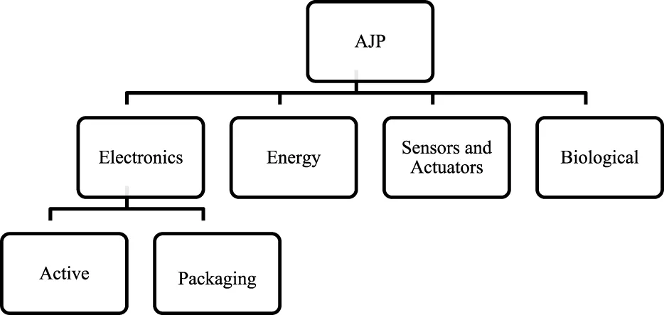
4.1 Electronics
AJP has demonstrated significant potential across various applications, from enhancing the efficiency of solar cells by over 1% in photovoltaics to more routine uses such as screen printing and cellphone case manufacturing (Yang et al., 2011; Krzemiński et al., 2021). The technology is versatile, accommodating a wide range of inks, thus making it applicable to numerous fields. In the realm of printed electronics, AJP excels in both active electronic applications and electronics packaging. For instance, Novo et al. designed a platform of six electrochemical sensors to detect and quantify glucose levels between 3 and 10 mM in clinical settings (Di Novo et al., 2019). Similarly, Serpelloni et al. printed hybrid smart devices like capacitive sensors and Surface Mount Devices (SMDs) on cellulose substrates such as chromatographic paper, photo paper, and cardboard, achieving a maximum resistivity of 26.3 × 10⁻⁸ Ω·m (Serpelloni et al., 2020). Vella et al. created a capacitive sensor with five touch points on a 3D curved surface, which could sense contact areas on these points (Vella et al., 2019). In another example, Arsenov et al. printed an X-band double-slot antenna on a PI substrate, operating at a frequency of 10.5 GHz (Arsenov et al., 2021). Lewis et al. highlighted the expanded possibilities in printed electronics due to AJP’s capability to print both conducting and insulating structures with a minimal offset from the substrate. They demonstrated this in the Internet of Things (IoT) domain using the Nordic Semiconductor nRF51822 Multiprotocol Bluetooth low energy/2.4 GHz RF System on Chip (SoC), which incorporates sensors, LEDs, actuators, and RF transmitters (Lewis et al., 2017).
Large-scale production of multifunctional printed electronics is plagued by several challenges, including the control of material transitions with precision and integration of intricate geometries. For example, transitioning between varying material compositions in high-volume additive manufacturing systems requires an in-depth understanding of how the materials are mixed to achieve uniform performance (Guo et al., 2019). Furthermore, the production of multifunctional 3D microelectronic devices is hindered by the requirement to obtain high geometric complexity and nanoscale precision. Mechanically guided 3D assembly and microfabrication techniques are proposed as solutions to these issues, providing versatile platforms for the integration of increased functions and functional component density (Brackett et al., 2021). In the field of printed interconnects, Gu et al. developed a novel method for producing high-frequency inductors for high-bandwidth radio frequency applications (Gu et al., 2019). Piekarz et al. (2019) printed interconnects for millimeter-wave applications using silver ink, finding these printed parts to be cost-effective solutions (Qayyum et al., 2017). Elmogi et al. replaced bonding wires in optical transmitter assemblies with printed silver interconnects, reporting improved functionality compared to aluminum bonding wires (Elmogi et al., 2018a). Oakley et al. (2017) fabricated, simulated, and characterized terahertz filters using AJP silver ink (Jahn et al., 2018). Goh et al. produced stretchable electronic devices like flexible circuits and strain gauges using silicone-silver composite ink (Serpelloni et al., 2020; Navratil et al., 2019; Vella et al., 2019; Efimov et al., 2018b; Gu et al., 2019; Lall et al., 2019b; Gupta et al., 2016; Stoukatch et al., 2012; Cantù et al., 2018a; Gräf et al., 2018; Röhrl et al., 2018; Azzopardi et al., 2019; Goh et al., 2018b). To enhance power converter efficiency and reduce size, high integration in power electronics is crucial. Azzopardi et al. created single-switch devices where bottom electrodes were connected through a silver layer deposited via AJP, achieving a resistivity of 12 mΩ with 16 layers. Laurent et al. and Smith et al. investigated the electrical properties of aerosol printed lines on various substrates, finding that thermal treatment improved electrical performance, making them suitable for electronic applications up to 1–2 MHz (Smith et al., 2017). Lomakin et al. used silver nano ink on a Rogers RO 4350 substrate to print microstrip transmission lines, applicable up to 67 GHz (Lomakin et al., 2018). He et al. and Pavec et al. printed antennas using silver nanoparticle ink, with Pavec et al. noting that layer heights impacted return loss while frequency remained stable (Pavec et al., 2019). Lall et al. studied the effect of process parameters on the consistency and dimensional accuracy of AJP over extended periods, measuring efficiency using process capability indices (Lall et al., 2019a). Gupta et al. fabricated photodetectors using zinc oxide nanocrystals, showing photo response in the ultraviolet spectrum of 250 nm–400 nm (A Gupta et al., 2018). Cardenas et al. examined the impact of silver contact morphology on carbon nanotube thin film transistors (CNT-TFT), noting its effect on device performance (Cardenas et al., 2018).
AJP has also demonstrated notable efficiency in electronics packaging, offering dimension flexibility for both 2D planar and non-planar substrates with printed thicknesses ranging from 1 μm to 10 μm. Craton et al. introduced the “chip-first” approach for packaging mm-wave devices, printing packages and interconnects on top of the die, achieving a worst-case loss of 0.290 dB at 40 GHz. In wafer-level packaging (WLP) (Zhan et al., 2015). Cai et al. (2016) successfully used AJP to print conductive inks and pastes directly onto packaged dies for shielding, leveraging AJP’s capability to stack layers with feature sizes as small as 20 μm in the xy-direction and 0.7 μm in the z-direction.
4.2 Sensors and actuators
Di Novo et al. utilized AJP to design and fabricate an electrochemical microfluidic device’s sensor platform without support structures. They successfully fabricated the intended platform, with the inner chamber made of several inks such as AgCl, carbon, and multiwalled carbon nanotubes, and the outer chamber incorporating a combination of AgCl and carbon inks (Di Novo et al., 2019). Borghetti et al. addressed the challenges of curvature and temperature sensitivity in AJP-printed sensors or electronics. They proposed printing Ag using the AJP method on a 3D non-planar surface and employing photonic sintering to mitigate overheating issues in plastic bodies. They demonstrated their concept by printing strain gauges on PVC conduit (Borghetti et al., 2019). Agarwala et al.a numerical study on strain sensors for future shape optimization, considering criteria like end loop dimensions, gauge length, and grid line specifications. Cantù et al. (2018a) explored the use of microsensors for protein detection and quantification, finding the AJP approach effective. Clifford et al. (2018) developed a relative humidity sensor with 0%–80% RH effectiveness by combining the AJP process and drop casting, using silver ink and Nafion respectively. Vella et al. (2019) used silver ink to create capacitive touch sensors on hollow cylindrical PVC, PC, and ABS tubing. Li et al. investigated the AJP process to fabricate a photo sensor with resistive memory advantages, using Tungsten diselenide (WSe2) as the primary element. They deposited Ag-WSe2-Ag and CNT-WSe2-CNT on flexible Kapton, followed by laser sintering, resulting in low switching power and voltage-derived resistive RAM compared to other flexible RAMs. Li et al. (2020) examined the dispersion effect during the fabrication of CNT-made bucky paper sensors for composite applications. Their sensors could detect resin flow or curing and respond to mechanical stress in the Vacuum Assisted Resin Transfer Molding (VARTM) process. Bolse et al. (2017) developed 12 types of fluorescence sensors from six different light-emitting polymer inks to detect explosive nitroaromatics like Nitrotoluene (NT), dinitrobenzene (DNB), and dinitrotoluene (DNT). Cho et al. (2019) focused on fabricating a metal oxide sensor using SnO2 through the AJP method, attaching it to micro hotplates derived from poly-MUMPs technology. Goh, Yeong, and Agarwala developed a pH level sensor using an AJP printer, first depositing CNT ink on polyimide film, followed by serpentine CNT layers, achieving remarkable pH detection performance. In actuator development, Wilkinson et al. (2019a) used carbon-based conductive ink to fabricate a series of actuators, employing image processing methods to examine the strain performance of several dielectric elastomer actuators printed with AJP.
4.3 Biological applications
Grunwald et al. evaluated the feasibility of using AJP for fabricating microarrays with DNA or protein-derived ink. They found that AJP-printed microarrays are more accurate than those produced by other printing technologies, even allowing for smaller sizes. AJP printing proved reliable for both planar and non-planar surfaces in applications involving sensor and biomolecule printing (Grunwald et al., 2010). Williams et al. demonstrated the use of AJP to print highly sensitive immunoassays using biological reagents on both planar and arbitrarily shaped surfaces. They addressed the hindering effects of ultrasonication, ensuring the stability and effectiveness of the printed biological reagents (Williams et al., 2020). These studies highlight AJP’s versatility and precision in bio-printing applications, paving the way for biosensors and other biomedical device advancements.
5 Process modeling and future directions in ink development
AJP’s process modeling is critical for understanding and controlling the printing quality. The historical approach has been to rely heavily on empirical observation, valuable as it is, lacking the underlying strength seen in more sophisticated printing technologies (Wilkinson et al., 2019b). Recent developments have introduced machine learning paradigms to enhance process modeling. For instance, a hybrid machine learning procedure has been developed to predict the best operating windows through search of design spaces and the simulation of the impact of significant parameters like sheath and carrier gas flow rates. The procedure leverages data-driven methodology to systematically seek the printing process optimally and offers a better substitute for the conventional trial-and-error method. AJP recipe optimization involves a modification of the process conditions and ink formulation to achieve optimal print properties. Machine learning has been instrumental in this area, where software employs support vector machines and Gaussian process regression to optimize line morphology and reduce overspray (Williams et al., 2020). The methods allow one to find the ideal operating conditions that can optimize conflicting objectives, i.e., maximize line thickness while minimizing edge roughness (Zhang et al., 2019). The use of multi-objective optimization tools further helps to attain the inherent trade-offs among various printed line characteristics for high-quality outcomes.
The development of inks for applications, such as wearable electronics and biosensors, is a rapidly developing field with tremendous potential to enhance the functionality of additive jet printing (AJP). This review addresses future trends in ink developments, focusing on hybrid inks for multi-material systems and their applications in emerging technologies. Hybrid inks, for instance, are gaining attention based on their prospect of merging various materials with variable properties to formulate complex, multi-faceted devices. By coupling digital light processing with direct ink writing, new composite architectures and devices with high-speed and high-resolution (Camargo et al., 2021; Peng et al., 2021) can be manufactured within a single printing process have been found to produce. This approach allows for the use of heterogeneous inks and resins as well as the production of functional composites with tunable mechanical properties and improved interface bonding, which are crucial for their uses in soft robotics and electronics (Peng et al., 2021). Ink development of wearable electronics’ tailor-made type is of utmost significance in technology development. Stable silk protein-stabilized carbon nanotube (CNT) inks have been shown to be stable and biocompatible, using which circuits might be printed on a variety of substrates such as plastics and clothing (Liang et al., 2020). Inks of this kind are particularly suited to the fabrication of smart wearable devices such as respiratory sensors and ECG electrodes due to their flexibility and biocompatibility (Liang et al., 2020). Similarly, inkjet printing has also been regarded as an efficient means of production for wearable electronics by virtue of its high efficiency, cost-effectiveness, and environment-friendly production (Yan et al., 2020; Gao et al., 2017). Inkjet printing facilitates exact deposition of the functional materials with the ability of producing flexible, durable wearable devices (Gao et al., 2017).
Conductive inks play a pivotal role in the production of electrochemical sensors and biosensors, essential for medical, environmental, and industrial monitoring. These inks, which are usually composed of nanostructured materials such as platinum, silver, and gold nanoparticles, offer better conductivity and flexibility in designing electrodes (Camargo et al., 2021). Carbon-based substances, such as graphene and carbon nanotubes, enhance the biocompatibility and functionality of these sensors, which allow them to be used in wearable devices (Camargo et al., 2021; Yang and Wang, 2016). MXene inks have shown excellent prospects for many applications owing to their exceptional electronic, optical, and mechanical characteristics. MXene inks are applicable for the synthesis of multifunctional devices such as electromagnetic shielding, Joule heaters, and piezoresistive sensors by applying screen printing techniques (Wu et al., 2022; Aghayar et al., 2022). MXene inks with superior conductivity and stability are also good candidates for potential smart and wearable devices (Aghayar et al., 2022).
AJP offers very good design freedom, allowing for the creation of 2D as well as 3D patterns with high precision. This versatility is necessary in the design of advanced electronic devices, such as ultrahigh-responsive photodetectors and flexible optoelectronics, which exploit the ability to print on flexible and non-planar substrates (Zhang et al., 2019). The functionality offered by printed electronics is enhanced by the ability to form high-quality, conformal patterns that can be incorporated into many applications, from wearable electronics to intelligent packaging. The future of ink formulation lies in the creation of hybrid inks and custom-designed formulations that cater to the needs of emerging applications such as wearable electronics and biosensors. These advancements have the potential to significantly enhance the functionality of AJP, enabling it to produce multifunctional, high-performance devices. As science advances, combining different materials and optimizing ink formulations will be the most significant drivers in realizing the full potential of this fast-changing field.
6 Conclusion
Even though it is the leading technology for highly accurate material deposition, particularly in microsystem devices manufacturing, Aerosol Jet Printing (AJP), still faces important technical and economic issues which are the main reasons why its industrial adoption is limited. One of the basic obstacles is the operational stability issue since AJP’s aerosolized deposition can become very sensitive to the environmental conditions such as humidity and air flow, thus resulting in print inconsistencies. Furthermore, the main disadvantages high cost and low throughput still exist, making it less appropriate for bulk production as compared to screen and gravure printing. Although AJP bestows unique advantages when it comes to treating difficult geometries and distinct material sets, having in mind that its gaseous sheath flow mechanism decreases nozzle clogging, it nonetheless calls for meticulous process optimization to obtain reproducible results. AJP’s fine feature resolution has really turned the tide in terms of printing conductive, semi-conductive, and biological materials, and this has made it a compelling option for flexible electronics, sensors, and biomedical devices. Not only that but the ability of AJP to print metallic nanoparticle-based and carbon-based inks has been the source of the most conductive nanoscale patterns ever, thus it is now useful in areas that were deemed beyond its reach.
Despite these limitations, continued progress in optimizing processes and material compositions has the potential to propel AJP to a breakthrough manufacturing position. By addressing scalability and cost-effectiveness, AJP might emerge as a more viable solution for industrial applications, allowing for high-precision micro-patterning not solely on planar surfaces but also on non-planar and flexible substrates, opening up novel opportunities in wearable electronics, bio-printing, and next-generation semiconductor manufacturing.
Statements
Author contributions
RE: Conceptualization, Data curation, Formal Analysis, Methodology, Visualization, Writing – original draft, Writing – review and editing. AR: Data curation, Investigation, Methodology, Resources, Writing – original draft. CS-U-Z: Investigation, Methodology, Resources, Writing – original draft. MK: Conceptualization, Funding acquisition, Project administration, Supervision, Validation, Writing – original draft, Writing – review and editing.
Funding
The author(s) declare that financial support was received for the research and/or publication of this article. MK acknowledges funding support from the Natural Sciences and Engineering Research Council of Canada (NSERC).
Acknowledgments
The authors express their gratitude to Vinay Patel, Islam Hassan, and P. Ravi Selvaganapathy for their assistance during the review process.
Conflict of interest
The authors declare that the research was conducted in the absence of any commercial or financial relationships that could be construed as a potential conflict of interest.
Generative AI statement
The authors declare that no Generative AI was used in the creation of this manuscript.
Publisher’s note
All claims expressed in this article are solely those of the authors and do not necessarily represent those of their affiliated organizations, or those of the publisher, the editors and the reviewers. Any product that may be evaluated in this article, or claim that may be made by its manufacturer, is not guaranteed or endorsed by the publisher.
Supplementary material
The Supplementary Material for this article can be found online at: https://www.frontiersin.org/articles/10.3389/fmtec.2025.1558209/full#supplementary-material
References
1
AbtM.RochA.QayyumJ. A.PestotnikS.StepienL.Abu-AgeelA.et al (2018). Aerosol-printed highly conductive Ag transmission lines for flexible electronic devices. IEEE Trans. Compon. Packag. Manuf. Technol.8, 1838–1844. 10.1109/TCPMT.2018.2869977
2
AdibM.EcksteinR.Hernandez-SosaG.SommerM.LemmerU. (2018). SnO2 nanowire-based aerosol jet printed electronic nose as fire detector. IEEE Sens. J.18, 494–500. 10.1109/JSEN.2017.2777178
3
AgaR.JordanC.AgaR. S.BartschC. M.HeckmanE. M. (2014). Metal electrode work function modification using aerosol jet printing. IEEE Electron Device Lett.35, 1124–1126. 10.1109/LED.2014.2355142
4
AgarwalaS.GohG. L.YeongW. Y. (2017). Optimizing aerosol jet printing process of silver ink for printed electronics. IOP Conf. Ser. Mater Sci. Eng.191, 012027. 10.1088/1757-899x/191/1/012027
5
AgarwalaS.Liang GohG.Dinh LeT.-S.AnJ.Kai PehZ.YeeY. W.et al (2018). Wearable bandage-based strain sensor for home healthcare: combining 3D aerosol jet printing and laser sintering. ACS Sens.4, 218–226. 10.1021/acssensors.8b01293
6
AgarwalaS.YeongW. Y. (2019). “Aerosol jet fabricated biodegradable antenna for bioelectronics application,” in Transactions on additive manufacturing meets medicine (Singapore: Nanyang Technological University). 10.18416/AMMM.2019.1909S02T02
7
AghayarZ.MalakiM.ZhangY. (2022). MXene-based ink design for printed applications. Nanomaterials12, 4346. 10.3390/nano12234346
8
A GuptaA.ArunachalamS.Cloutier SG.IzquierdoR. (2018). Fully aerosol-jet printed, high-performance nanoporous ZnO ultraviolet photodetectors. ACS Photonics5, 3923–3929. 10.1021/acsphotonics.8b00829
9
AndrewsJ. B.CaoC.BrookeM. A.FranklinA. D. (2017). Noninvasive material thickness detection by aerosol jet printed sensors enhanced through metallic carbon nanotube ink. IEEE Sens. J.17, 4612–4618. 10.1109/JSEN.2017.2710085
10
ArsenovP. V.SobolevA. S.EfimovA. A.IvanovV. V. (2021). Double slot aerosol jet printed antenna for X-band applications. J. Phys. Conf. Ser.2086, 012047. 10.1088/1742-6596/2086/1/012047
11
ArsenovP. V.VlasovI. S.EfimovA. A.MinkovK. N.IvanovV. V. (2019). Aerosol jet printing of platinum microheaters for the application in gas sensors. IOP Conf. Ser. Mater Sci. Eng.473, 012042. 10.1088/1757-899x/473/1/012042
12
AzzopardiS.LelièvreJ.YoussefT.LabrousseD.PereiraE.LasserreP. (2019). “Aerosol jet printing process for semi-embedded power assembly,” in 2019 IEEE international workshop on integrated power packaging (IWIPP), 68–72. 10.1109/IWIPP.2019.8799091
13
BagS.DeneaultJ. R.DurstockM. F. (2017). Aerosol-jet-assisted thin-film growth of CH3NH3PbI3 perovskites—a means to achieve high quality, defect-free films for efficient solar cells. Adv. Energy Mater7:1701151. 10.1002/aenm.201701151
14
BendoniR.SangiorgiN.SangiorgiA.SansonA. (2015). Role of water in TiO2 screen-printing inks for dye-sensitized solar cells. Sol. Energy122, 497–507. 10.1016/J.SOLENER.2015.09.025
15
BlumenthalT.FratelloV.NinoG.RitalaK. (2017). Aerosol Jet® printing onto 3D and flexible substrates. WA, United States: Kent.
16
BolseN.EcksteinR.SchendM.HabermehlA.Hernandez-SosaG.EschenbaumC.et al (2017). “Discrimination of trace nitroaromatics using linear discriminant analysis on aerosol jet printed fluorescent sensor arrays,” in Optical sensors 2017. Editors BaldiniF.HomolaJ.LiebermanR. A. (Prague, Czech Republic: SPIE), 10231, 102310R–102330R. 10.1117/12.2265522
17
BorghettiM.SerpelloniM.SardiniE. (2019). Printed strain gauge on 3D and low-melting point plastic surface by aerosol jet printing and photonic curing. Sensors19, 4220. 10.3390/s19194220
18
BrackettJ.YanY.CauthenD.KishoreV.LindahlJ.SmithT.et al (2021). Characterizing material transitions in large-scale Additive Manufacturing. Addit. Manuf.38, 101750. 10.1016/j.addma.2020.101750
19
CaiF.ChangY.WangK.KhanW. T.PavlidisS.PapapolymerouJ. (2014). “High resolution aerosol jet printing of D-band printed transmission lines on flexible LCP substrate,” in IEEE MTT-S international microwave symposium (IMS2014) (Tampa, FL), 1–3. 10.1109/MWSYM.2014.6848597
20
CaiF.ChangY. H.WangK.ZhangC.WangB.PapapolymerouJ. (2016). Low-loss 3-D multilayer transmission lines and interconnects fabricated by additive manufacturing technologies. IEEE Trans. Microw. Theory Tech.64, 3208–3216. 10.1109/TMTT.2016.2601907
21
CalvertP. (2001). Inkjet printing for materials and devices. Chem. Mater.13, 3299–3305. 10.1021/cm0101632
22
CamargoJ. R.OrzariL. O.AraújoD. A. G.de OliveiraP. R.KalinkeC.RochaD. P.et al (2021). Development of conductive inks for electrochemical sensors and biosensors. Microchem. J.164, 105998. 10.1016/j.microc.2021.105998
23
CantùE.TonelloS.AbateG.UbertiD.SardiniE.SerpelloniM. (2018b). Aerosol jet printed 3D electrochemical sensors for protein detection. Sensors18, 3719. 10.3390/s18113719
24
CantùE.TonelloS.SerpelloniM.SardiniE. (2018a). “Aerosol jet printed sensors for protein detection: a preliminary study,” in Proceedings of the fourth national conference on sensors, catania, ItalyAndòB.BaldiniF.Di NataleC.FerrariV.MarlettaV.MarrazzaG. (Springer International Publishing), 317–327. 10.1007/978-3-030-04324-7_40
25
CaoC.AndrewsJ. B.FranklinA. D. (2017). Completely printed, flexible, stable, and hysteresis-free carbon nanotube thin-film transistors via aerosol jet printing. Adv. Electron Mater3, 1700057. 10.1002/aelm.201700057
26
CapelA. J.SmithM. A. A.TaccolaS.Pardo-FiguerezM.RimingtonR. P.LewisM. P.et al (2021). Digitally driven aerosol jet printing to enable customisable neuronal guidance. Front. Cell Dev. Biol.9, 722294. 10.3389/fcell.2021.722294
27
CardenasJ. A.UpshawS.CatenaccrM. J.WileyB. J.FranklinA. D. (2018). “Exploring silver contact morphologies in printed carbon nanotube thin-film transistors,” in 2018 76th device research conference (DRC), 1–2. 10.1109/DRC.2018.8442217
28
CendraC.GaoT.LeeK. Y. (2017). Standard operating procedure of Optomec aerosol jet printer in pneumatic atomizer mode and characterization of printed PEDOT:PSS lines.
29
ChoY.-C.ElsayedM. Y.El-GamalM. N. (2019). “A metal-oxide gas sensor based on an aerosol jet printing technology featuring a one second response time,” in 2019 20th international conference on solid-state sensors, actuators and microsystems eurosensors XXXIII (TRANSDUCERS EUROSENSORS XXXIII), 1333–1336. 10.1109/TRANSDUCERS.2019.8808446
30
CliffordB.BeynonD.PhillipsC.DeganelloD. (2018). Printed-Sensor-on-Chip devices – aerosol jet deposition of thin film relative humidity sensors onto packaged integrated circuits. Sens. Actuators B Chem.255, 1031–1038. 10.1016/J.SNB.2017.08.086
31
CooperC.HughesB. (2020). Aerosol jet printing of electronics: an enabling technology for wearable devices. Pan pacific microelectronics symposium (Pan pacific), HI, USA: 2020, p. 1–11. 10.23919/PanPacific48324.2020.9059444
32
CratonM. T.SorockiJ.PiekarzI.GruszczynskiS.WinczaK.PapapolymerouJ. (2018). “Realization of fully 3D printed W-band bandpass filters using aerosol jet printing technology,” in 2018 48th European microwave conference (EuMC), 1013–1016. 10.23919/EuMC.2018.8541416
33
DalalN.GuY.ChenG.HinesD. R.DasguptaA.DasS. (2019). Effect of gas flow rates on quality of aerosol jet printed traces with nanoparticle conducting ink. J. Electron Packag142, 011012. 10.1115/1.4044960
34
DatarA. (2012). Micro-extrusion process parameter modeling. Masters. Rochester Institute of Technology. Available online at: https://repository.rit.edu/cgi/viewcontent.cgi?article=6714&context=theses.
35
DeganelloD.CherryJ. A.GethinD. T.ClaypoleT. C. (2010). Patterning of micro-scale conductive networks using reel-to-reel flexographic printing. Thin Solid Films518, 6113–6116. 10.1016/J.TSF.2010.05.125
36
DegryseO.BloemenV.FerrarisE. (2022). Collagen composite inks for Aerosol Jet® printing in bone tissue engineering applications. Procedia CIRP110, 180–185. 10.1016/j.procir.2022.06.033
37
DeinerL. J.JenkinsT.HowellT.RottmayerM. (2019b). Aerosol jet printed polymer composite electrolytes for solid-state Li-ion batteries. Adv. Eng. Mater21, 1900952. 10.1002/adem.201900952
38
DeinerL. J.JenkinsT.PowellA.HowellT.RottmayerM. (2019a). High capacity rate capable aerosol jet printed Li-ion battery cathode. Adv. Eng. Mater. 21, 1801281. 10.1002/adem.201801281
39
DeinerL. J.ReitzT. L. (2017). Inkjet and aerosol jet printing of electrochemical devices for energy conversion and storage. Adv. Eng. Mater19, 1600878. 10.1002/adem.201600878
40
DelageA.DelhoteN.VerdeymeS.BonnetB.CarpentierL.SchickC.et al (2018). Aerosol jet printing of millimeter wave transmission lines on 3D ceramic substrates made by additive manufacturing. IEEE/MTT-S Int. Microw. Symp. - IMS, Phila. PA, 1557–1560. 10.1109/MWSYM.2018.8439498
41
Di NovoN. G.CantùE.TonelloS.SardiniE.SerpelloniM. (2019). Support-material-free microfluidics on an electrochemical sensors platform by aerosol jet printing. Sensors19, 1842. 10.3390/s19081842
42
DrewK.HopmanS.HörteisM.GlunzS. W.GranekF. (2011). Combining laser chemical processing and aerosol jet printing: a laboratory scale feasibility study. Prog. Photovoltaics Res. Appl.19, 253–259. 10.1002/pip.1014
43
EcksteinR. (2016). Aerosol jet printed electronic devices and systems. Karlsruhe Institute of Technology. Doctoral. 10.5445/IR/1000065424
44
EcksteinR.RödlmeierT.GlaserT.ValouchS.MauerR.LemmerU.et al (2015). Aerosol-jet printed flexible organic photodiodes: semi-transparent, color neutral, and highly efficient. Adv. Electron Mater1, 1500101. 10.1002/aelm.201500101
45
EfimovA.PotapovG.NisanA.UrazovM.IvanovV. (2017). Application of the spark discharge generator for solvent-free aerosol jet printing. Orient. J. Chem.33, 1047–1050. 10.13005/ojc/330264
46
EfimovA. A.ArsenovP. V.MinkovK. N.IvanovV. V. (2018b). Fabrication of metallic lines by aerosol jet printing: study of the effect of substrate temperature on the aspect ratio. Orient. J. Chem.34, 2777–2781. 10.13005/ojc/340613
47
EfimovA. A.MinkovK. N.ArsenovP. V.ProtasN. V.IvanovV. V. (2018a). Investigation of sintering of silver lines on a heated plastic substrate in the dry aerosol jet printing. IOP Conf Ser. J. Phys. Conf Ser.1124, 081041. 10.1088/1742-6596/1124/8/081041
48
ElmogiA.RamonH.LambrechtJ.OssieurP.TorfsG.MissinneJ.et al (2018a). Aerosol-jet printed interconnects for 60-Gb/s CMOS driver and microring modulator transmitter assembly. IEEE Photonics Technol. Lett.30, 1944–1947. 10.1109/LPT.2018.2873056
49
ElmogiA.SoenenW.RamonH.YinX.MissinneJ.SpigaS.et al (2018b). Aerosol-jet printed interconnects for 2.5 D electronic and photonic integration. J. Light. Technol.36, 3528–3533. 10.1109/JLT.2018.2848699
50
ElmogiA.WugS.EugB.MissinneJ.SpigaS.AmannM.-C.et al (2017). “Flexible hybrid integration of photonic and electronic chips using aerosol-jet printing,” in 22nd annual symposium of the IEEE photonics society benelux chapter, 82–85.
51
FengJ. Q. (2017). A computational study of particle deposition patterns from a circular laminar jet. J. Appl. Fluid Mech.10, 1001–1012. 10.18869/acadpub.jafm.73.241.27233
52
FengJ. Q.RennM. J. (2019). Aerosol Jet® direct-write for microscale additive manufacturing. J. Micro Nanomanuf7. 10.1115/1.4043595
53
FisherC.SkolroodL. N.LiK.JoshiP. C.AytugT. (2023). Aerosol-jet printed sensors for environmental, safety, and health monitoring: a review. Adv. Mater Technol.8. 10.1002/admt.202300030
54
GagnéL.RiveraG.LarocheG. (2006). Micropatterning with aerosols: application for biomaterials. Biomaterials27, 5430–5439. 10.1016/J.BIOMATERIALS.2006.06.006
55
GaoM.LiL.SongY. (2017). Inkjet printing wearable electronic devices. J. Mater Chem. C Mater5, 2971–2993. 10.1039/c7tc00038c
56
GohG. L.AgarwalaS.TanY. J.YeongW. Y. (2018c). A low cost and flexible carbon nanotube pH sensor fabricated using aerosol jet technology for live cell applications. Sens. Actuators B Chem.260, 227–235. 10.1016/J.SNB.2017.12.127
57
GohG. L.AgarwalaS.YeongW. Y. (2018b). “High resolution aerosol jet printing of conductive ink for stretchable electronics,” in Proceedings of the 3rd international conference on progress in additive manufacturing (Singapore: Nanyang Technological University), 109–114. 10.25341/D4FS3W
58
GohG. L.YeongW. Y.AgarwalaS. (2018a). Aerosol jet printed pH sensor based on carbon nanotubes for flexible electronics. Proceedings of the 3rd international conference on progress in additive manufacturing, Singapore: Nanyang Technological University. p. 88–94. 10.25341/D4Q59F
59
GothC.PutzoS.FrankeJ. (2011). “Aerosol Jet printing on rapid prototyping materials for fine pitch electronic applications,” in 2011 IEEE 61st electronic components and technology conference (ECTC)Lake Buena Vista, FL, 1211–1216. 10.1109/ECTC.2011.5898664
60
GräfD.NeermannS.StuberL.ScheetzM.JöF. (2018). “Pushing the boundaries of 3D-MID: pulse-width modulated light technology for enhancing surface properties and enabling printed electronics on FFF-printed structures,” in 2018 13th international congress molded interconnect devices (MID), würzburg, Germany, 1–5. 10.1109/ICMID.2018.8526995
61
GrunwaldI.GrothE.WirthI.SchumacherJ.MaiwaldM.ZoellmerV.et al (2010). Surface biofunctionalization and production of miniaturized sensor structures using aerosol printing technologies. Biofabrication2, 014106. 10.1088/1758-5082/2/1/014106
62
GuD.ShiX.PopraweR.BourellD. L.SetchiR.ZhuJ. (1979). Material-structure-performance integrated laser-metal additive manufacturing. Science2021, eabg1487. 10.1126/science.abg1487
63
GuY.HinesD. R.YunV.AntoniakM.DasS. (2017). Aerosol-jet printed fillets for well-formed electrical connections between different leveled surfaces. Adv. Mater Technol.2:1700178. 10.1002/admt.201700178
64
GuY.ParkD.GonyaS.JendrisakJ.DasS.HinesD. R. (2019). Direct-write printed broadband inductors. Addit. Manuf.30, 100843. 10.1016/J.ADDMA.2019.100843
65
GuoX.XueZ.ZhangY. (2019). Manufacturing of 3D multifunctional microelectronic devices: challenges and opportunities. NPG Asia Mater11, 29. 10.1038/s41427-019-0129-7
66
GuptaA. A.BolducA.CloutierS. G.IzquierdoR. (2016). “Aerosol Jet Printing for printed electronics rapid prototyping,” in 2016 IEEE international symposium on circuits and systems (ISCAS), 866–869. 10.1109/ISCAS.2016.7527378
67
HabermehlA.EcksteinR.StrobelN.BolseN.Hernandez-SosaG.MertensA.et al (2017). Microfluidic surface-enhanced Raman analysis systems by aerosol jet printing: towards low-cost integrated sensor systems. IEEE SENSORS, 1–3. 10.1109/ICSENS.2017.8234346
68
HeC.JinN.YuH.LinJ.MaC. Q. (2019). The electrical sintering and fusing effects of Aerosol-Jet printed silver conductive line. Mater Lett.246, 5–8. 10.1016/J.MATLET.2019.03.016
69
HeY.CratonM. T.ChahalP.PapapolymerouJ. (2018). A Bi-material fully aerosol jet printed W-band quasi-yagi-uda antenna. Boulder, CO:1–3. 10.1109/GSMM.2018.8439233
70
HeY.OakleyC.ChahalP.AlbrechtJ. D.PapapolymerouJ. (2017). Aerosol Jet printed 24 GHz end-fire quasi-Yagi-Uda antenna on a 3-D printed cavity substrate. Int. Workshop Antenna Technol. Small Antennas, Innovative Struct. Appl. (iWAT), 179–182. 10.1109/iwat.2017.7915352
71
HedgesM.MartinA. B. (2012). “3D aerosol Jet® printing - adding electronics functionality to RP/RM,” in Fraunhofer direct digital manufacturing conference, 1–5. Berlin, Germany.
72
HesterJ.NguyenE.TiceJ.RadisicV. (2017). “A novel 3D-printing-enabled “roller coaster” transmission line,” in 2017 IEEE international symposium on antennas and propagation USNC/URSI national radio science meeting, 2639–2640. 10.1109/APUSNCURSINRSM.2017.8073362
73
HoerberJ.GothC.FrankeJ.HedgesM. (2011). Electrical functionalization of thermoplastic materials by aerosol jet printing. p. 813–818. 10.1109/EPTC.2011.6184525
74
HoffmannG.WolferT.ReitbergerT.LorenzL.WolterK.-J.FrankeJ.et al (2016). Combination of flexographic and aerosol jet printing for integrated polymer op-tical step index waveguides. Proc. 117th Annu. Meet. DGaO, Hanover, Ger. Deutsche Gesellschaft für angewandte Optik (DGaO), A11–A117.
75
HohnholzA.ObataK.NakajimaY.KochJ.TerakawaM.SuttmannO.et al (2019). Hybrid UV laser direct writing of UV-curable PDMS thin film using aerosol jet printing. Appl. Phys. A125, 120. 10.1007/s00339-018-1902-0
76
HsuT.-R. (2002). Miniaturization - a paradigm shift in advanced manufacturing and education.
77
HuangQ.ZhuY. (2019). Printing conductive nanomaterials for flexible and stretchable electronics: a review of materials, processes, and applications. Adv. Mater Technol.4, 1800546. 10.1002/admt.201800546
78
HuangY.JiangL.LiB.PremaratneP.JiangS.QinH. (2020). Study effects of particle size in metal nanoink for electrohydrodynamic inkjet printing through analysis of droplet impact behaviors. J. Manuf. Process56, 1270–1276. 10.1016/j.jmapro.2020.04.021
79
HueblerA. C.DoetzF.KempaH.KatzH. E.BartzschM.BrandtN.et al (2007). Ring oscillator fabricated completely by means of mass-printing technologies. Org. Electron8, 480–486. 10.1016/J.ORGEL.2007.02.009
80
IDS (2025). Integrated deposition solutions. Inc. Available online at: https://www.idsnm.com/(Accessed February 2, 2022).
81
IhleM.ZiescheS.ZechC.BaumannB. (2019). “Functional printing of MMIC-interconnects on LTCC packages for sub-THz applications,” in 2019 22nd European microelectronics and packaging conference exhibition (EMPC), 1–4. 10.23919/EMPC44848.2019.8951799
82
JabariE.ToyserkaniE. (2015). Micro-scale aerosol-jet printing of graphene interconnects. Carbon N. Y.91, 321–329. 10.1016/J.CARBON.2015.04.094
83
JabariE.ToyserkaniE. (2016). Aerosol-Jet printing of highly flexible and conductive graphene/silver patterns. Mater Lett.174, 40–43. 10.1016/J.MATLET.2016.03.082
84
JahnD.EcksteinR.SchneiderL. M.BornN.Hernandez-SosaG.BalzerJ. C.et al (2018). Digital aerosol jet printing for the fabrication of terahertz metamaterials. Adv. Mater Technol.3, 1700236. 10.1002/admt.201700236
85
JingQ.ChoiY. S.SmithM.ĆatićN.OuC.Kar-NarayanS. (2019a). Aerosol-jet printed fine-featured triboelectric sensors for motion sensing. Adv. Mater Technol.4, 1800328. 10.1002/admt.201800328
86
JingQ.ChoiY. S.SmithM.OuC.BusoloT.Kar-NarayanS. (2019b). Freestanding functional structures by aerosol-jet printing for stretchable electronics and sensing applications. Adv. Mater Technol.4, 1900048. 10.1002/admt.201900048
87
JohannesS. J.KeicherD. M.LavinJ. M.SecorE. B.WhettenS. R.EssienM. (2018). “Multimaterial aerosol jet printing of passive circuit elements,” in Proceedings of the 29th annual international solid freeform fabrication symposium (Austin, Texas: The University of Texas at Austin), 473–478.
88
JordanC. D.ThorneB. R. H.WadhwaA.LoseyA. D.OzhinskyE.KondapavulurS.et al (2020). Wireless resonant circuits printed using aerosol jet deposition for MRI catheter tracking. IEEE Trans. Biomed. Eng.67, 876–882. 10.1109/TBME.2019.2922879
89
KaindlR.GuptaT.BlümelA.PeiS.HouP. X.DuJ.et al (2021). Aerosol jet printing of graphene and carbon nanotube patterns on realistically rugged substrates. ACS Omega6, 34301–34313. 10.1021/acsomega.1c03871
90
KhanS.NguyenT. P.LubejM.ThieryL.VairacP.BriandD. (2018). Low-power printed micro-hotplates through aerosol jetting of gold on thin polyimide membranes. Microelectron. Eng.194, 71–78. 10.1016/J.MEE.2018.03.013
91
KhanS.NguyenT. P.ThieryL.VairacP.BriandD. (2017). Aerosol jet printing of miniaturized, low power flexible micro-hotplates. Eurosensors1, 316. 10.3390/proceedings1040316
92
KhondokerM. A. H.MunS. C.KimJ. (2013). Synthesis and characterization of conductive silver ink for electrode printing on cellulose film. Appl. Phys. A Mater Sci. Process112, 411–418. 10.1007/s00339-012-7419-z
93
KhorramdelB.TorkkeliA.MäNtysaloM. (2018). Electrical contacts in SOI MEMS using aerosol jet printing. IEEE J. Electron Devices Soc.6, 34–40. 10.1109/JEDS.2017.2764498
94
KimS.MoonH.KwonH.LeeG.YuD.ChoiJ.et al (2019). Organic vapor-jet printing with reduced heat transfer for fabrication of flexible organic devices. Adv. Mater Technol.4, 1800332.10.1002/admt.201800332
95
KingB. H.O’ReillyM. J.BarnesS. M. (2009). “Characterzing aerosol Jet® multi-nozzle process parameters for non-contact front side metallization of silicon solar cells,” in 2009 34th IEEE photovoltaic specialists conference (PVSC), 1107–1111. 10.1109/PVSC.2009.5411213
96
KingB. H.RennM. (2009). Aerosol Jet direct write printing for mil-aero electronic applications. Palo Alto, CA.
97
KopolaP.ZimmermannB.FilipovicA.SchleiermacherH. F.GreulichJ.RousuS.et al (2012). Aerosol jet printed grid for ITO-free inverted organic solar cells. Sol. Energy Mater. Sol. Cells107, 252–258. 10.1016/J.SOLMAT.2012.06.042
98
KrzemińskiJ.DominiczakJ.BaranieckiD.JanczakD.RaczyńskiT.OstapkoJ.et al (2021). Printability of collecting electrode using ajp for new construction of photovoltaic device. Cryst. (Basel)11, 1184. 10.3390/cryst11101184
99
KrzeminskiJ.KanthamneniA.WagnerD.DetertM.SchmidtB.JakubowskaM. (2018). Microscale hybrid flexible circuit printed with aerosol jet technique. IEEE Trans. Nanotechnol.17, 979–984. 10.1109/TNANO.2018.2841639
100
KrzeminskiJ.KrzeminskiJ.JakubowskaM.KanthamneniA.WagnerD.DetertM.et al (2017a). Pads and microscale vias with aerosol jet printing technique. 21st Eur. Microelectron. Packag. Conf. (EMPC) Exhib. Warsaw, Pol., 1–4. 10.23919/EMPC.2017.8346869
101
KrzeminskiJ.WroblewskiG.Dybowska-SarapukL.LepakS.JakubowskaM. (2017b). “Nanosilver conductive lines made by spray coating and aerosol jet printing technique,” in Proceedings of photonics applications in astronomy, communications, industry, and high energy physics experiments. Editors RomaniukR. S.LinczukM. (Wilga, Poland: SPIE), 10445, 1528–1533. 10.1117/12.2280836
102
KuoL.SangwanV. K.RangnekarS. V.ChuT. C.LamD.ZhuZ.et al (2022). All-printed ultrahigh-responsivity MoS2 nanosheet photodetectors enabled by megasonic exfoliation. Adv. Mater.34, e2203772. 10.1002/adma.202203772
103
LaiD. W. (2017). Aerosol jet printing of selective molecular inks for patterning of 2D MoS2. Master’s. University of Dayton.
104
LallP.AbrolA.KothariN.LeeverB.MillerS. (2019a). “Effect of print parameters on print consistency of aerosol jet printed electronics,” in 2019 18th IEEE intersociety conference on thermal and thermomechanical phenomena in electronic systems (ITherm). Las Vegas, NV, 633–642. 10.1109/ITHERM.2019.8757268
105
LallP.GoyalK.LeeverB.MillerS. (2019b). “Factors influencing the line consistency of commonly used geometries for additively printed electronics,” in 2019 18th IEEE intersociety conference on thermal and thermomechanical phenomena in electronic systems (ITherm) (Las Vegas, NV), 863–869. 10.1109/ITHERM.2019.8757308
106
LanX.LuX.ChenM. Y.ScherrerD.ChungT.NguyenE.et al (2017). Direct on-chip 3-D aerosol jet printing with high reliability. IEEE Trans. Compon. Packag. Manuf. Technol.7, 1369–1376. 10.1109/TCPMT.2017.2710957
107
LandgrafM.ReitelshöferS.FrankeJ.HedgesM. (2013). “Aerosol jet printing and lightweight power electronics for dielectric elastomer actuators,” in 2013 3rd international electric drives production conference (EDPC) (Nuremberg, Germany), 1–7. 10.1109/EDPC.2013.6689733
108
LangfordN.ShinaS. (2019). Using conformal printed electronics for 3D printed antenna systems building blocks, Kauai, HI, p. 1–16. 10.23919/PanPacific.2019.8696768
109
LaurentP.StoukatchS.DupontF.KraftM. (2018). Electrical characterization of Aerosol Jet Printing (AJP) deposited conductive silver tracks on organic materials. Microelectron. Eng.197, 67–75. 10.1016/J.MEE.2018.06.002
110
LeeA.SudauK.Hyun AhnK.Jong LeeS.WillenbacherN. (2012). Optimization of experimental parameters to suppress nozzle clogging in inkjet printing. Industrial and Eng. Chem. Res.51, 13195–13204. 10.1021/ie301403g
111
LemmerU.StrobelN.LehrJ.EcksteinR.Hernandez-SosaG.RödlmeierT. (2018). “From printed organic photodiodes to printed image sensors (Conference Presentation),” in Organic and hybrid sensors and bioelectronics XI. Editors KymissisI.ShinarR.TorsiL.List-KratochvilE. J. W. (San Diego, CA: SPIE), 10738, 5. 10.1117/12.2321689
112
LewisP.WhiteR.Smith -DraperB. (2017). L essons learned in the implementation of aerosol jet printing for fabricating multilayer circuit boards.
113
LiB.ClarkP. A.ChurchK. H. (2007). “Robust direct-write dispensing tool and solutions for micro/meso-scale manufacturing and packaging,” in ASME 2007 International Manufacturing Science and Engineering Conference. 715–721. 10.1115/MSEC2007-31037
114
LiY.FengX.SivanM.LeongJ. F.TangB.WangX.et al (2020). Aerosol jet printed WSe2 crossbar architecture device on Kapton with dual functionality as resistive memory and photosensor for flexible system integration. IEEE Sens. J.20, 4653–4659. 10.1109/JSEN.2020.2966547
115
LiY.SivanM.NiuJ. X.VeluriH.ZamburgE.LeongJ.et al (2019). “Aerosol jet printed WSe2 based RRAM on Kapton suitable for flexible monolithic memory integration,” in 2019 IEEE international conference on flexible and printable sensors and systems (FLEPS)1–3. 10.1109/FLEPS.2019.8792256
116
LiangX.LiH.DouJ.WangQ.HeW.WangC.et al (2020). Stable and biocompatible carbon nanotube ink mediated by silk protein for printed electronics. Adv. Mater.32, e2000165. 10.1002/adma.202000165
117
LiuR.DingH.LinJ.ShenF.CuiZ.ZhangT. (2012). Fabrication of platinum-decorated single-walled carbon nanotube based hydrogen sensors by aerosol jet printing. Nanotechnology23, 505301. 10.1088/0957-4484/23/50/505301
118
LiuR.ShenF.DingH.LinJ.GuW.CuiZ.et al (2013). All-carbon-based field effect transistors fabricated by aerosol jet printing on flexible substrates. J. Micromechanics Microengineering23, 065027. 10.1088/0960-1317/23/6/065027
119
LomakinK.SippelM.GoldG.FröhlichJ.HelmreichK.AnkenbrandM.et al (2018). “Low reflective aerosol Jet printed broadband matched load up to 67 GHz,” in 2018 11th German microwave conference (GeMiC), 379–382. 10.23919/GEMIC.2018.8335109
120
LorenzL.NieweglowskiK.WolterK.-J.BockK.HoffmannG.-A.OvermeyerL.et al (2017). Additive waveguide manufacturing for optical bus couplers by aerosol jet printing using conditioned flexible substrates. 21st Eur. Microelectron. Packag. Conf. (EMPC) Exhib. Warsaw, Pol., 1–5. 10.23919/EMPC.2017.8346857
121
LuS.Cardenas JA.WorsleyR.WilliamsN.Andrews JB.CasiraghiC.et al (2019). Flexible, print-in-place 1D–2D thin-film transistors using aerosol jet printing. ACS Nano13, 11263–11272. 10.1021/acsnano.9b04337
122
MadouM. J. (2018). Fundamentals of microfabrication: the science of miniaturization. Second Edition. Chapman and Hall: CRC Press.
123
MahajanA.Daniel FrisbieC.Francis LF. (2013). Optimization of aerosol jet printing for high-resolution, high-aspect ratio silver lines. ACS Appl. Mater. and Interfaces5, 4856–4864. 10.1021/am400606y
124
MaherM.SmithA.MargiottaJ. (2014). “A synopsis of the Defense Advanced Research Projects Agency (DARPA) investment in additive manufacture and what challenges remain,”. Laser 3D manufacturing. Editors HelvajianH.PiquéA.WegenerM.GuB. (SPIE), 8970, 897002–897009. 10.1117/12.2044725
125
McKibbenN.CurtisM.MaryonO.SawyerM.LazouskayaM.EixenbergerJ.et al (2024). Formulation and aerosol jet printing of nickel nanoparticle ink for high-temperature microelectronic applications and patterned graphene growth. ACS Appl. Electron Mater6, 748–760. 10.1021/acsaelm.3c01175
126
Mendes-FelipeC.OliveiraJ.EtxebarriaI.Vilas-VilelaJ. L.Lanceros-MendezS. (2019). State-of-the-Art and future challenges of UV curable polymer-based smart materials for printing technologies. Adv. Mater Technol.4. 10.1002/admt.201800618
127
MetteA.RichterP. L.HörteisM.GlunzS. W. (2007). Metal aerosol jet printing for solar cell metallization. Prog. Photovoltaics Res. Appl.15, 621–627. 10.1002/pip.759
128
MuralidharanR.RajA.SivasubramonyR. S.YadavM.AlhendiM.NilssonM.et al (2019). Effect of substrate properties on isothermal fatigue of aerosol jet printed nano-Ag traces on flex. J. Mater Res.34, 2903–2910. 10.1557/jmr.2019.226
129
NavratilJ.HamacekA.RebounJ.SoukupR. (2015). “Perspective methods of creating conductive paths by Aerosol Jet Printing technology,” in 2015 38th international spring seminar on electronics technology (ISSE), eger, Hungary, 36–39. 10.1109/ISSE.2015.7247957
130
NavratilJ.RerichaT.SmitkaV.HamacekA. (2019). “Double sided printed pattern interconnected by aerosol jet and NCA technologies,” in 42nd international spring seminar on electronics technology (ISSE), 1–4. 10.1109/ISSE.2019.8810265
131
OakleyC.AlbrechtJ. D.PapapolymerouJ.ChahalP. (2019). Low-loss aerosol-jet printed wideband interconnects for embedded devices. IEEE Trans. Compon. Packag. Manuf. Technol.9, 2305–2313. 10.1109/TCPMT.2019.2933792
132
OakleyC.KaurA.ByfordJ. A.ChahalP. (2017). “Aerosol-jet printed quasi-optical terahertz filters,” in 2017 IEEE 67th electronic components and technology conference (ECTC), 248–253. 10.1109/ECTC.2017.233
133
ObataK.KlugU.KochJ.SuttmannO.OvermeyerL. (2014). Hybrid micro-stereo-lithography by means of aerosol jet printing technology. J. Laser Micro/Nanoeng.9, 242–247. 10.2961/jlmn.2014.03.0012
134
ObataK.SchonewilleA.SlobinS.HohnholzA.UngerC.KochJ.et al (2017). Hybrid 2D patterning using UV laser direct writing and aerosol jet printing of UV curable polydimethylsiloxane. Appl. Phys. Lett.111, 121903. 10.1063/1.4996547
135
OptomecO. (2022). Production equipment and digital solutions for the additive age. Available online at: https://optomec.com/(Accessed February 2, 2022).
136
OuC. (2020). Aerosol-jet printed nanocomposites for flexible and stretchable thermoelectric generators. Apollo - University of Cambridge. 10.17863/CAM.50693
137
OuC.SangleA. L.ChalklenT.JingQ.NarayanV.Kar-NarayanS. (2018). Enhanced thermoelectric properties of flexible aerosol-jet printed carbon nanotube-based nanocomposites. Apl. Mater6, 96101. 10.1063/1.5043547
138
OuyangJ.CormierD.WilliamsS. A.BorkholderD. A. (2016). Photonic sintering of aerosol jet printed lead zirconate titanate (PZT) thick films. J. Am. Ceram. Soc.99, 2569–2577. 10.1111/jace.14272
139
PaulsenJ. A.RennM.ChristensonK.PlourdeR. (2012). “Printing conformal electronics on 3D structures with Aerosol Jet technology,” in 2012 future of instrumentation international workshop (FIIW) proceedings, gatlinburg, TN, 1–4. 10.1109/FIIW.2012.6378343
140
PavecM.NavratilJ.SoukupR.SmitkaV.HamacekA. (2019). “Fully printed IoT antenna for drone-deployed autonomous sensor unit,” in 2019 42nd international spring seminar on electronics technology (ISSE), wroclaw, Poland, 1–4. 10.1109/ISSE.2019.8810226
141
PengX.KuangX.RoachD. J.WangY.HamelC. M.LuC.et al (2021). Integrating digital light processing with direct ink writing for hybrid 3D printing of functional structures and devices. Addit. Manuf.40, 101911. 10.1016/j.addma.2021.101911
142
PhuahE.LangleyD.CastroJ. O.YeoL. Y.SumerH.StoddartP. R. (2019). “Aerosol jet bioprinting,” in Australian biomedical engineering conference: technology and research in Australian medical science (Melbourne, Australia: Engineers Australia), 17.
143
PhuahE. W. C.HartW. L.SumerH.StoddartP. R. (2020). Patterning of biomaterials by aerosol jet printing: a parametric study. Bioprinting18, e00081. 10.1016/J.BPRINT.2020.E00081
144
PiekarzI.SorockiJ.CratonM. T.WinczaK.GruszczynskiS.PapapolymerouJ. (2019). Application of aerosol jet 3-D printing with conductive and nonconductive inks for manufacturing mm-wave circuits. IEEE Trans. Compon. Packag. Manuf. Technol.9, 586–595. 10.1109/TCPMT.2018.2889698
145
PuetzJ.AegerterM. A. (2008). Direct gravure printing of indium tin oxide nanoparticle patterns on polymer foils. Thin Solid Films516, 4495–4501. 10.1016/J.TSF.2007.05.086
146
QayyumJ. A.AbtM.RochA.UlusoyA. C.PapapolymerouJ. (2017). “Ultra wideband 3D interconnects using aerosol jet printing up to 110 GHz,” in 2017 12th European microwave integrated circuits conference (EuMIC), 372–375. 10.23919/EuMIC.2017.8230736
147
RahmanM. T.McCloyJ.RamanaC. V.PanatR. (2016). Structure, electrical characteristics, and high-temperature stability of aerosol jet printed silver nanoparticle films. J. Appl. Phys.120, 75305. 10.1063/1.4960779
148
ReitbergerT.FrankeJ.HoffmannG.-A.OvermeyerL.LorenzL.WolterK.-J. (2016b). “Integration of polymer optical waveguides by using flexographic and aerosol jet printing,” in 2016 12th international congress molded interconnect devices (MID) (Wuerzburg, Germany), 1–6. 10.1109/ICMID.2016.7738933
149
ReitbergerT.HoffmannG.-A.WolferT.OvermeyerL.FrankeJ. (2016a). “Printing polymer optical waveguides on conditioned transparent flexible foils by using the aerosol jet technology,” in Printed memory and circuits II. Editor List-KratochvilE. J. W. (San Diego, CA: SPIE), 9945, 99450G–99524G. 10.1117/12.2236220
150
ReitelshöferS.GöttlerM.SchmidtP.TrefferP.LandgrafM.FrankeJ. (2016). “Aerosol-Jet-Printing silicone layers and electrodes for stacked dielectric elastomer actuators in one processing device,” in Electroactive polymer actuators and devices (EAPAD) 2016. Editors Bar-CohenY.VidalF. (NV: SPIE: Las Vegas), 9798, 350–358. 10.1117/12.2219226
151
RennM. J.KingB. H. (2005). Forming structures using aerosol jet® deposition. US9607889B2.
152
RennM. J.MarquezG.KingB. H.EssienM.DoyleM. W. (2002). Flow- and laser-guided direct write of electronic and biological components. Direct-Write Technol. Rapid Prototyp., 475–492. 10.1016/B978-012174231-7/50068-3
153
RochaV. G.García-TuñónE.BotasC.MarkoulidisF.FeildenE.D’EliaE.et al (2017). Multimaterial 3D printing of graphene-based electrodes for electrochemical energy storage using thermoresponsive inks. ACS Appl. Mater Interfaces9, 37136–37145. 10.1021/acsami.7b10285
154
RöhrlF. X.JakobJ.BognerW.WeigelR.ZornS. (2018). “Bare die connections via aerosol jet technology for millimeter wave applications,” in 2018 48th European microwave conference (EuMC), 1033–1036. 10.23919/EuMC.2018.8541697
155
RoscherF.ThalheimR.SeifertT.PaulS.-D.ZichnerR.WiemerM.et al (2019). “Joining two worlds - hybrid integration of silicon based electronics and printed functionalities,” in Smart systems integration; 13th international conference and exhibition on integration issues of miniaturized systems, 1–8.
156
RudorferA.TschernerM.PalfingerC.ReilF.HartmannP.SeferisI. E.et al (2016). “A study on Aerosol jet printing technology in LED module manufacturing,” in Fifteenth international conference on solid state lighting and LED-based illumination systems. Editors KaneM. H.DietzN.FergusonI. T. (San Diego, CA: SPIE), 9954, 52–59. 10.1117/12.2237737
157
Saeidi-JavashM.KuangW.DunC.ZhangY. (2019). 3D conformal printing and photonic sintering of high-performance flexible thermoelectric films using 2D nanoplates. Adv. Funct. Mater. 29, 1901930. 10.1002/adfm.201901930
158
SaengchairatN.TranT.ChuaC.-K. (2017). A review: additive manufacturing for active electronic components. Virtual Phys. Prototyp.12, 31–46. 10.1080/17452759.2016.1253181
159
SalaryR.LombardiJ. P.Samie TootooniM.DonovanR.RaoP. K.BorgesenP.et al (2017). Computational fluid dynamics modeling and online monitoring of aerosol jet printing process. J. Manuf. Sci. Eng.139, 021015. 10.1115/1.4034591
160
SalaryR. R.LombardiI. I. I. J. P.WeerawarneD. L.RaoP. K.PoliksM. D. (2019). “A state-of-the-art review on aerosol jet printing (AJP) additive manufacturing process,” in ASME 2019 14th international manufacturing science and engineering conference, 1–16. 10.1115/MSEC2019-3008
161
SalehM. S.HuC.PanatR. (2017). Three-dimensional microarchitected materials and devices using nanoparticle assembly by pointwise spatial printing. Sci. Adv.3, e1601986. 10.1126/sciadv.1601986
162
SaundersR. E.DerbyB. (2014). Inkjet printing biomaterials for tissue engineering: bioprinting. Int. Mater. Rev.59, 430–448. 10.1179/1743280414Y.0000000040
163
SecorE. B. (2018). Principles of aerosol jet printing. Flexible Print. Electron.3, 035002. 10.1088/2058-8585/aace28
164
SerpelloniM.CantùE.BorghettiM.SardiniE. (2020). Printed smart devices on cellulose-based materials by means of aerosol-jet printing and photonic curing. Sensors20, 841. 10.3390/s20030841
165
SettiL.PianaC.BonazziS.BallarinB.FrascaroD.Fraleoni-MorgeraA.et al (2004). Thermal inkjet technology for the microdeposition of biological molecules as a viable route for the realization of biosensors. Anal. Lett.37, 1559–1570. 10.1081/AL-120037587
166
ShankarR.AmertA.KellarJ. J.WhitesK. W. (2013). Silver nano-ink for aerosol-jet (M3D) printed solar electrodes. Nanomater. Energy2, 20–24. 10.1680/nme.12.00025
167
ShiJ.CagneyN.TatumJ.CondieA.Rafael Castrejon-PitaJ. (2024). Jetting and droplet formation of particle-loaded fluids. Phys. Fluids36. 10.1063/5.0180014
168
ShteinM.PeumansP.BenzigerJ. B.ForrestS. R. (2004). Direct mask-free patterning of molecular organic semiconductors using organic vapor jet printing. J. Appl. Phys.96, 4500–4507. 10.1063/1.1791760
169
SiddiqueS.ParkJ. G.AndreiP.LiangR. (2019). M3D aerosol jet printed buckypaper multifunctional sensors for composite structural health monitoring. Results Phys.13, 102094. 10.1016/J.RINP.2019.02.030
170
SmithM.ChoiY. S.BougheyC.Kar-NarayanS. (2017). Controlling and assessing the quality of aerosol jet printed features for large area and flexible electronics. Flexible Print. Electron.2, 015004. 10.1088/2058-8585/aa5af9
171
SoukupR.NavratilJ.RebounJ.RerichaT. (2015). “A comparison of the interdigital electrodes prepared by aerosol jet printing and lift-off technique,” in 2015 38th international spring seminar on electronics technology (ISSE), 30–35. 10.1109/ISSE.2015.7247956
172
StoukatchS.DupontF.SeronveauxL.VandormaelD.KraftM. (2017). “Additive low temperature 3D printed electronic as enabling technology for IoT application,” in 2017 IEEE 19th electronics packaging technology conference (EPTC), 1–6. 10.1109/EPTC.2017.8277554
173
StoukatchS.LaurentP.DricotS.AxisaF.SeronveauxL.VandormaelD.et al (2012). “Evaluation of Aerosol Jet Printing (AJP) technology for electronic packaging and interconnect technique,” in 2012 4th electronic system-integration technology conference, 1–5. 10.1109/ESTC.2012.6542067
174
SukeshiniA. M.MeisenkothenF.GardnerP.ReitzT. L. (2013). Aerosol Jet® Printing of functionally graded SOFC anode interlayer and microstructural investigation by low voltage scanning electron microscopy. J. Power Sources224, 295–303. 10.1016/J.JPOWSOUR.2012.09.094
175
SunH.WangK.LiY.ZhangC.JinR. (2017). Quality modeling of printed electronics in aerosol jet printing based on microscopic images. J. Manuf. Sci. Eng.139. 10.1115/1.4035586
176
TaitJ. G.WitkowskaE.HiradeM.KeT. H.MalinowskiP. E.SteudelS.et al (2015). Uniform Aerosol Jet printed polymer lines with 30 μm width for 140 ppi resolution RGB organic light emitting diodes. Org. Electron22, 40–43. 10.1016/J.ORGEL.2015.03.034
177
TanH. W.TranT.ChuaC. K. (2016). A review of printed passive electronic components through fully additive manufacturing methods. Virtual Phys. Prototyp.11, 271–288. 10.1080/17452759.2016.1217586
178
TarabellaG.VurroD.LaiS.D’AngeloP.AscariL.IannottaS. (2020). Aerosol jet printing of {PEDOT}:{PSS} for large area flexible electronics. Flexible Print. Electron.5, 14005. 10.1088/2058-8585/ab61c4
179
ThompsonB.YoonH.-S. (2013). Aerosol-printed strain sensor using PEDOT:PSS. IEEE Sens. J.13, 4256–4263. 10.1109/JSEN.2013.2264482
180
Tirado-GarciaI.Garcia-GonzalezD.Garzon-HernandezS.RusinekA.RoblesG.Martinez-TarifaJ. M.et al (2021). Conductive 3D printed PLA composites: on the interplay of mechanical, electrical and thermal behaviours. Compos Struct.265, 113744. 10.1016/j.compstruct.2021.113744
181
TuL.YuanS.ZhangH.WangP.CuiX.WangJ.et al (2018). Aerosol jet printed silver nanowire transparent electrode for flexible electronic application. J. Appl. Phys.123, 174905. 10.1063/1.5028263
182
TummalaR. (2001). Fundamentals of microsystems packaging. McGraw-Hill.
183
VandormaelD.RigoO.SeronveauxL.MonnoyeD.BeeckmanE.DormalT.et al (2012). “Direct deposition of surface acoustic wave sensors by aerosol jet printing technique,” in 6th international conference \\and exhibition on integration issues of miniaturized systems - MEMS, NEMS, ICs and electronic components, smart systems integration, 1–8. Session VII, Paper 32.
184
VasilievA. A.NisanA. V.SamotaevN. N. (2017). Aerosol/ink jet printing technology for high-temperature MEMS sensors. Proc. Eurosensors1, 617. 10.3390/proceedings1040617
185
VellaS.SmithsonC.HalfyardK.ShenE.ChrétienM. (2019). Integrated capacitive sensor devices aerosol jet printed on 3D objects. Flex. Print. Electron.4, 045005. 10.1088/2058-8585/ab59c0
186
VerheeckeW.Van DyckM.VogelerF.VoetA.ValkenaersH. (2012). “Optimizing aerosol jet printing of silver interconnects on polyimide film for embedded electronics applications,” in 8th international DAAAM baltic conference industrial engineering (Tallinn, Estonia: Tallinn University of Technology), 373–379.
187
VlnieskaV.GilshteinE.KunkaD.HeierJ.RomanyukY. E. (2022). Aerosol jet printing of 3D pillar arrays from photopolymer ink. Polym. (Basel)14, 3411. 10.3390/polym14163411
188
WangC.HongG.-Y.LiK.-M.YoungH.-T. (2017). A miniaturized nickel oxide thermistor via aerosol jet technology. Sensors17, 2602. 10.3390/s17112602
189
WangK.ChangY. H.ZhangC.WangB. (2016). Conductive-on-demand: tailorable polyimide/carbon nanotube nanocomposite thin film by dual-material aerosol jet printing. Carbon N. Y.98, 397–403. 10.1016/J.CARBON.2015.11.032
190
WeiL. J.OxleyC. H. (2016). Carbon based resistive strain gauge sensor fabricated on titanium using micro-dispensing direct write technology. Sens. Actuators A Phys.247, 389–392. 10.1016/J.SNA.2016.06.025
191
WilkinsonN. J.Lukic-MannM.ShuttleworthM. P.KayR. W.HarrisR. A. (2019a). “Aerosol jet printing for the manufacture of soft robotic devices,” in 2019 2nd IEEE international conference on soft robotics (RoboSoft), 496–501. 10.1109/ROBOSOFT.2019.8722766
192
WilkinsonN. J.SmithM. A. A.KayR. W.HarrisR. A. (2019b). A review of aerosol jet printing—a non-traditional hybrid process for micro-manufacturing. Int. J. Adv. Manuf. Technol.105, 4599–4619. 10.1007/s00170-019-03438-2
193
WilliamsN. X.WatsonN.JohD. Y.ChilkotiA.FranklinA. D. (2020). Aerosol jet printing of biological inks by ultrasonic delivery. Biofabrication12, 025004. 10.1088/1758-5090/ab5cf5
194
Williams BA.MahajanA.Smeaton MA.Holgate CS.Aydil ES.Francis LF. (2015). Formation of copper zinc tin sulfide thin films from colloidal nanocrystal dispersions via aerosol-jet printing and compaction. ACS Appl. Mater. and Interfaces7, 11526–11535. 10.1021/acsami.5b02484
195
WinarskiD. ∼J.KreitE.HeckmanE. ∼M.FlesburgE.HasemanM.AgaR. ∼S.et al (2018). Photoconductive ZnO films printed on flexible substrates by inkjet and aerosol jet techniques. J. Electron Mater47, 949–954. 10.1007/s11664-017-5903-0
196
WuH.XieY.MaY.ZhangB.XiaB.ZhangP.et al (2022). Aqueous MXene/xanthan gum hybrid inks for screen-printing electromagnetic shielding, Joule heater, and piezoresistive sensor. Small18. 10.1002/smll.202107087
197
XiaY.SiJ.LiZ. (2016). Fabrication techniques for microfluidic paper-based analytical devices and their applications for biological testing: a review. Biosens. Bioelectron.77, 774–789. 10.1016/J.BIOS.2015.10.032
198
XieW.ZhangX.LeightonC.FrisbieC. D. (2017). 2D insulator–metal transition in aerosol-jet-printed electrolyte-gated indium oxide thin film transistors. Adv. Electron Mater3, 1600369. 10.1002/aelm.201600369
199
YanK.LiJ.PanL.ShiY. (2020). Inkjet printing for flexible and wearable electronics. Apl. Mater8. 10.1063/5.0031669
200
YangC.ZhouE.MiyanishiS.HashimotoK.TajimaK. (2011). Preparation of active layers in polymer solar cells by aerosol jet printing. ACS Appl. Mater Interfaces3, 4053–4058. 10.1021/am200907k
201
YangW.WangC. (2016). Graphene and the related conductive inks for flexible electronics. J. Mater Chem. C Mater4, 7193–7207. 10.1039/c6tc01625a
202
Zare BidokyF.Daniel FrisbieC. (2016). Parasitic capacitance effect on dynamic performance of aerosol-jet-printed sub 2 V poly(3-hexylthiophene) electrolyte-gated transistors. ACS Appl. Mater. and Interfaces8, 27012–27017. 10.1021/acsami.6b08396
203
ZhanZ.YuL.WeiJ.ZhengC.SunD.WangL. (2015). Application of Aerosol Jet technology in through-via interconnection for MEMS wafer-level packaging. Microsyst. Technol.21, 451–455. 10.1007/s00542-014-2107-x
204
ZhangH.HongE.ChenX.LiuZ. (2022). Machine learning enables process optimization of aerosol jet 3D printing based on the droplet morphology. ACS Appl. Mater Interfaces. 10.1021/acsami.2c21476
205
ZhangH.MoonS. K.NgoT. H. (2019). Hybrid machine learning method to determine the optimal operating process window in aerosol jet 3D printing. ACS Appl. Mater Interfaces11, 17994–18003. 10.1021/acsami.9b02898
206
ZhangH.MoonS. K.NgoT. H.TouJ. (2025). Rapid process modeling of the aerosol jet printing based on Gaussian process regression with Latin hypercube sampling. Int. J. Precis. Eng. Manuf. 123AD21, 127–136. 10.1007/s12541-019-00237-3
207
ZhaoD.LiuT.ParkJ. G.ZhangM.ChenJ. M.WangB. (2012b). Conductivity enhancement of aerosol-jet printed electronics by using silver nanoparticles ink with carbon nanotubes. Microelectron. Eng.96, 71–75. 10.1016/J.MEE.2012.03.004
208
ZhaoJ.GaoY.GuW.WangC.LinJ.ChenZ.et al (2012a). Fabrication and electrical properties of all-printed carbon nanotube thin film transistors on flexible substrates. J. Mater Chem.22, 20747–20753. 10.1039/C2JM34598F
209
ZhouL.ZhuangJ. Y.SongM. S.SuW. M.CuiZ. (2014). Enhanced performance for organic light-emitting diodes by embedding an aerosol jet printed conductive grid. J. Phys. D. Appl. Phys.47, 115504. 10.1088/0022-3727/47/11/115504
210
ZollmerV.MullerM.RennM.BusseM.WirthI.CodlinskiD.et al (2006). Printing with aerosol: a maskless deposition technique allows high definition printing of a variety of functional material. Eur. Coatings J.7–8, 46–55.
Summary
Keywords
aerosol jet printing, microdroplets, atomization, sheath flow, non-planar, ultrasonic
Citation
Elsersawy R, Rahman A, Sakib-Uz-Zaman C and Khondoker MAH (2025) Multifunctional inks in aerosol jet printing: performance, challenges, and applications. Front. Manuf. Technol. 5:1558209. doi: 10.3389/fmtec.2025.1558209
Received
09 January 2025
Accepted
17 April 2025
Published
01 May 2025
Volume
5 - 2025
Edited by
Rahul Davis, Technology and Sciences, India
Reviewed by
Ran Jin, Virginia Tech, United States
Kunal Mondal, Oak Ridge National Laboratory (DOE), United States
Updates
Copyright
© 2025 Elsersawy, Rahman, Sakib-Uz-Zaman and Khondoker.
This is an open-access article distributed under the terms of the Creative Commons Attribution License (CC BY). The use, distribution or reproduction in other forums is permitted, provided the original author(s) and the copyright owner(s) are credited and that the original publication in this journal is cited, in accordance with accepted academic practice. No use, distribution or reproduction is permitted which does not comply with these terms.
*Correspondence: Mohammad Abu Hasan Khondoker, mohammad.khondoker@uregina.ca
Disclaimer
All claims expressed in this article are solely those of the authors and do not necessarily represent those of their affiliated organizations, or those of the publisher, the editors and the reviewers. Any product that may be evaluated in this article or claim that may be made by its manufacturer is not guaranteed or endorsed by the publisher.