 Stefan Scholze Stefan Schiefer
 Johannes Partzsch Stephan Hartmann
 Christian Georg Mayr*
 Sebastian Höppner Holger Eisenreich Stephan Henker
 Bernhard Vogginger and Rene Schüffny
- Chair of Highly-Parallel VLSI-Systems and Neuromorphic Circuits, Technische Universität Dresden, Dresden, Germany
State-of-the-art large-scale neuromorphic systems require sophisticated spike event communication between units of the neural network. We present a high-speed communication infrastructure for a waferscale neuromorphic system, based on application-specific neuromorphic communication ICs in an field programmable gate arrays (FPGA)-maintained environment. The ICs implement configurable axonal delays, as required for certain types of dynamic processing or for emulating spike-based learning among distant cortical areas. Measurements are presented which show the efficacy of these delays in influencing behavior of neuromorphic benchmarks. The specialized, dedicated address-event-representation communication in most current systems requires separate, low-bandwidth configuration channels. In contrast, the configuration of the waferscale neuromorphic system is also handled by the digital packet-based pulse channel, which transmits configuration data at the full bandwidth otherwise used for pulse transmission. The overall so-called pulse communication subgroup (ICs and FPGA) delivers a factor 25–50 more event transmission rate than other current neuromorphic communication infrastructures.
1 Introduction
The last years have seen a steady increase in the size of neuromorphic systems in order to handle progressively more advanced computational tasks (Giulioni et al., 2008; Serrano-Gotarredona et al., 2009; Schemmel et al., 2010). These large-scale hardware systems for spiking neural networks require high-speed communication for transmitting spike events between the different units of the neural network. Several communication/interface boards based on commercial field programmable gate arrays (FPGA) have been developed in recent years, commonly employing the address-event-representation (AER) protocol for pulse transmission (Berge and Häfliger, 2007; Fasnacht et al., 2008; Serrano-Gotarredona et al., 2009). Those designs were predominantly optimized for asynchronous operation and low latency, whereas demands on integration density and bandwidth were relatively relaxed. There are also some systems that employ application-specific digital ICs (Mayr et al., 2006; Merolla et al., 2007) which achieve a high throughput and integration density, but their configurability is naturally limited to the amount predesigned into the ICs.
However, there is currently no solution which combines integration density, high-speed, low latency, and configurability. A combination of these characteristics is especially required when moving to a large-scale hardware system, such as the waferscale neuromorphic hardware depicted in Figure 1, which has been developed in the FACETS project (Ehrlich et al., 2007) and is currently being completed in the follow-on project BrainScaleS. This system employs waferscale integration technology to gain a high connection density thereby implementing 40 million synapses and up to 180 k neurons. Furthermore, it is designed for operating at a speed-up factor of 104 compared to biological real-time, which increases simulation speed and integration density of the analog neuron and synapse circuits at the same time (Schemmel et al., 2010).
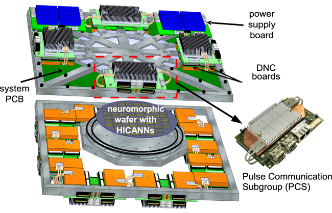
Figure 1. Overview of one wafer module of the FACETS/BrainScaleS waferscale neuromorphic system (Schemmel et al., 2010).
We have developed a communication infrastructure (Hartmann et al., 2010) for this waferscale neuromorphic system centered around a application-specific digital neuromorphic communication IC, called digital network chip (DNC; Scholze et al., 2011). The DNC–FPGA-assembly is called a pulse communication subgroup (PCS, see Figure 1). In contrast to conventional parallel asynchronous AER interfaces, the FPGA–DNC-wafer communication chain employs a significantly more versatile source-synchronous high-speed serial packet communication of time-stamped spike events. Such a packet-based network is advantageous for spike transmission, because it efficiently copes with the large number of sources and targets of the waferscale neuromorphic system, exploiting the limited bandwidth of the single transmission channels and offering flexible configuration of the connectivity between the units. Transmission of digital data packets also enables the system to embed the complete configuration information for the neuromorphic wafer in the regular spike data stream. This constitutes a significant advantage over other current systems, which usually employ separate configuration interfaces.
The time-stamped nature of the pulse packets allows configurable delays, which play key roles in various kinds of neuromorphic computation (Meyer et al., 2008; Deco et al., 2009). We use the synfire chain model of Kremkow et al. (2010) to show that the delay settings which are possible in our PCS constitute an advantageous feature in an actual neuromorphic computation experiment.
Section 2.1 gives an overview of the system and derives the specifications for the DNC based on the overall waferscale neuromorphic system. The single building blocks of the PCS (i.e., the DNC, FPGA, and other board components) are detailed in Section 2.2. Section 2.3 introduces the measurement setup used for both the raw communication test and the neuromorphic verification. Measured results for both test cases and a comparison to the state-of-the-art in pulse communication is given in Section 3.
2 Materials and Methods
2.1 The Waferscale Neuromorphic System
2.1.1 Waferscale neuromorphic system overview
The FACETS/BrainScaleS waferscale neuromorphic system consists of several wafer modules, depicted in Figure 1. The wafer sits on a system PCB which provides the electrical linkages to the outside. The system PCB in turn houses the PCSs, which provide the data and configuration communication to the wafer. The wafer modules have been designed for integrating a maximum of neurons and synapses at sufficient flexibility for connectivity and model parametrization. As a consequence of the speed-up factor, the resulting pulse frequencies call for dedicated, high-speed pulse communication. This is achieved by a two-layer approach: On the wafer, individual synapse-and-neuron blocks, called high input count analog neural networks (HICANNs; Ehrlich et al., 2007), are connected by a high-density routing grid (Schemmel et al., 2010). This on-wafer communication is complemented by a packet-based off-wafer network, connecting the wafer to the surrounding system and to other wafers. The main building blocks of this packet-based off-wafer network are the DNCs, which are situated on the PCS. As the packet-based network is the only communication link to/from the wafer, it has to provide pulse stimulation and monitoring as well as control and configuration of all the circuits on the wafer via the same links.
This packet-based off-wafer communication is hierarchically organized as shown in Figure 2. Eight of the HICANNs are placed on one reticle on the wafer. Communication streams from eight HICANNs are bundled in one DNC. In turn, four DNCs are situated on and communicate with one custom-designed FPGA board (Hartmann et al., 2010), forming the PCS. This tree-like structure enables one FPGA to control 32 HICANNs on the wafer via 4 DNCs. Overall, a single wafer requires 12 PCSs (Schemmel et al., 2010).
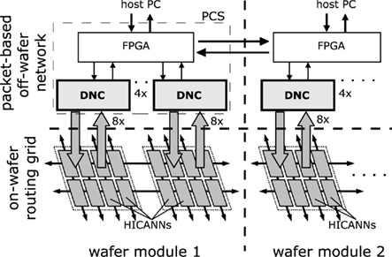
Figure 2. Logical structure of the off-wafer packet-based network and the on-wafer routing grid.
The off-wafer packet-based network is somewhat similar to the broadcast-mesh architecture of Merolla et al. (2007), with distributed PCSs each hooked up to a certain number of neuromorphic chips, while also being connected to four other PCSs, forming a packet routing network. However, by applying both DNC and FPGA to event routing, in contrast to Merolla et al. (2007) our architecture aims to achieve a combination of the traits of IC and FPGA, namely integration density, low latency and a wide range of configurability.
2.1.2 Communication requirements
The architecture of the packet-based network was chosen for two reasons: geometrical restrictions and distribution of the high overall bandwidth, which is discussed in the following. Since the analog neuron and synapse circuits on the wafer can not be suspended, the spike event transmission can not be slowed down. Thus, the spikes generated in the system have to be handled in technical real-time, making the spike rates and delays the main constraints for the system design. However, a priori calculation of event rates is an almost impossible task, because firing rates are largely dependent on the individual parametrization of the neurons in the network (Brunel, 2000). To still extract an estimate, in the following, we derive the number of spike sources (i.e., sending neurons) that send from or to a single wafer and assume a reasonable mean spike rate of 10 Hz for each of them.
These numbers can be derived from the connectivity of the neural network to be emulated on the hardware. Commonly, a neuron has one axonal output, but receives inputs from many other neurons via its synapses. In consequence, the inputs to the neurons on the wafer (i.e., the senders to the wafer) constitute the critical case, because they are much more numerous than the neurons’ outputs (i.e., the sender from the wafer) and largely dependent on the connection structure of the network. As each neuron has exactly one output, the number of spike sources that send from the wafer is equal to the number of neuron circuits on all the HICANNs. Each HICANN hosts up to 512 neurons, whose outputs may have to be transmitted to other locations in the off-wafer network. Considering the speed-up factor of 104, a total of 51.2 Mevent/s need to be transmitted from a single HICANN. For a whole wafer with 352 HICANNs (Schemmel et al., 2010), this adds up to 18 × 105 spike sources with 18 Gevent/s event rate.
For minimizing the total bandwidth requirements of the off-wafer network, single spike events are transmitted only to one HICANN per wafer and distributed locally on the wafer via the on-wafer routing grid. In this case, the number of senders to a single wafer is equal to the number of different external neurons that form a connection to at least one neuron on the wafer. The connectivity of the target neural network crucially determines this number. A worst-case scenario, i.e., a maximum of senders, results from uniformly distributed connectivity, e.g., represented by a uniform random graph (Brunel, 2000; Newman, 2003): In this case, the probability of an external neuron to form a connection with at least one of the neurons on the wafer would tend to 1. In consequence, the number of senders to the wafer would increase linearly with the number of neurons in the network (Partzsch and Schüffny, 2011). This growth is only bounded by the total amount of synapses on the wafer, because each of them can be only driven by one sending neuron. However, feeding each of the 40 million synapses with a separate external spike source would require an infeasible bandwidth.
A more biologically realistic network topology are locally connected networks (Mehring et al., 2003), which furthermore result in a bounded input count per wafer. A common assumption is a uniform distribution of neurons in a two-dimensional space and a Gaussian-shaped connection probability function:

with d denoting the Euclidean distance between two neurons and σ determining the extension of the Gaussian function. Because the connection probability diminishes with increasing distance, it is reasonable to assume that no connections exist outside a k·σ-interval, with the constant k determining the completeness of this assumption. Consequently, if the neurons on a wafer are located in a quadratical area with side length a in the two-dimensional space, all senders to the wafer are located in a boundary area A with width kσ around, as illustrated in Figure 3. In a multi-wafer-system, wafers would implement adjacent quadratic regions of neurons in the two-dimensional neuron field of Figure 3. A single wafer would have external connections from other wafers insofar as that the boundary area of this wafer encompasses neurons from the other wafers. The number of inputs T to the wafer can be estimated as:

with ρ denoting the neuron density. This value can be normalized with the mean number of synapses S per neuron, determined from p(d) by S = 2πσ2·ρ. Furthermore, we assume a fully utilized wafer, using all its Swaf = 4 · 107 available synapses. Accordingly, we calculate the number of neurons Nwaf that are placed on the wafer and the placement area from the number of synapses S per neuron: Swaf = Nwaf·S = ρa2·S. This results in:

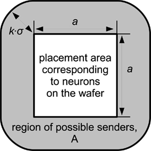
Figure 3. Approximation for the region of senders to a single wafer for locally connected networks.
Thus, the number of external senders, T, is only dependent on the number of synapses per neuron S, as shown in Figure 4. The graphs confirm that if the number of synapses per neuron is limited, as is the case for the wafer module: S ≤ Smax = 14336 (Schemmel et al., 2010), also the number of inputs to the wafer is bounded. For the 5σ-interval (k = 5), the estimate reaches up to 2.3 × 10⁵ external inputs. However, this is an overestimate, because not all neurons in the boundary region actually send to the quadratical area. Thus, the same number as for upstream transmission, 1.8 · 105, can be regarded as sufficient. This also allows for a symmetric design of the communication links.
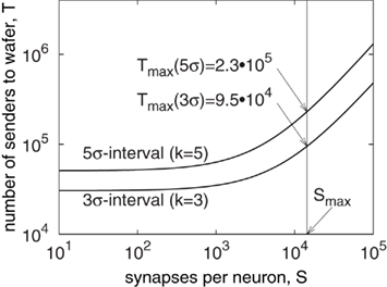
Figure 4. Number of external spike sources for a fully utilized wafer with Gaussian (local) connectivity.
Besides the spike rate of a neural connection, its (axonal) transmission delay is a crucial property that can significantly influence processing and adaptation behavior (Izhikevich et al., 2004). This delay is commonly assumed to be constant and in the order of several milliseconds (Hill and Tononi, 2005). With the introduced speed-up factor, this translates to some 100 ns in the system time domain, so that the latency of the communication links has to be taken into account. Also, the packet routing network, while effectively utilizing bandwidth and offering high flexibility, introduces variable, unpredictable delays due to packet prioritization and buffering. To counter this, pulse event packets contain a 15-bit timestamp denoting the arrival time at the target neuron on the wafer. This allows to buffer and sort the pulses at the final network node (i.e., DNC) until a target delay is reached (Scholze et al., 2010). This is in contrast to real-time neuromorphic hardware systems, where transmission delays are neglected (Fasnacht et al., 2008) or handled by a discretized system update (Jin et al., 2008). At the same time, this offers the possibility of configuring individual delays based on the timestamp. This complements the on-wafer routing grid, where pulses are transmitted almost instantaneously without any configurable delaying.
2.2 The Pulse Communication Subgroup
2.2.1 Digital network chip
As mentioned, the DNC provides communication between the FPGA and up to eight HICANNs. The DNC delivers pulse events originating in the host controller or the off-wafer communication network and coming via the FPGA as stimulus data for the waferscale neuromorphic hardware. In the other direction, it transmits pulse events from the HICANN as readout or for further transmission across the system. As the number of connections between the HICANNs on the wafer and the outside is limited by physical constraints, a minimal communication interface to the connected DNC is required. Using low-voltage differential signaling (LVDS) at double-data-rate (DDR; ANS, 2001), a raw data bandwidth of 2 Gbit/s is realized at a clock frequency of 1 GHz for each DNC–HICANN connection. The serial communication is source-synchronous, i.e., the physical connection consists of two differential lines (one clock line and one data line) for each direction of a DNC–HICANN connection. All HICANNs together thus produce data with a maximum bandwidth of 16 Gbit/s per direction across the DNC. A matching 16 Gbit/s data rate is provided by the DNC–FPGA connection, with 16 LVDS data lines together with 1 LVDS clock line running at a frequency of 500 MHz.
The system overview of the DNC is depicted in Figure 5. Each connection consists of the corresponding LVDS transceiver, the serializer, and deserializer circuits, responsible for the parallel to serial conversion and the link packet control that implements a packet protocol for the different types of data with error detection and correction mechanisms. The content of the packets, i.e., the pulse events and the configuration data, is handled in each of the eight HICANN connection modules. A novel VLSI implementation of an ordered heap (Scholze et al., 2010) compensates for the variable-delay packet routing by reordering the pulse events toward the HICANN based on their timestamps. These timestamps are generated in the HICANNs by reading out a system time counter each time a pulse is sent to the DNC. Before forwarding the pulse to the FPGA, the DNC adds a target transmission delay to this timestamp, which can be configured individually for each neuron address, allowing for individual axonal delays. Timestamps can be further modified in the FPGA, e.g., for realizing an individual latency for each DNC target of an axon. In biological terms, this corresponds to differing delays of axonal branches. The timestamp resolution is 4 ns, determined by the internal 250 MHz operating frequency of the DNC and HICANN.
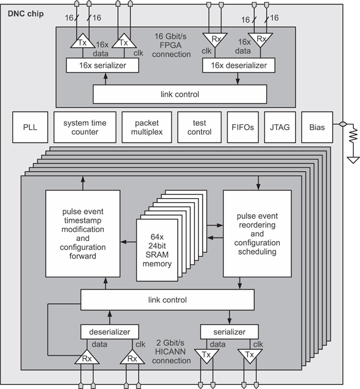
Figure 5. Block diagram of DNC with its eight HICANN interfaces and the FPGA connection (Scholze et al., 2011).
The configuration packets are directly inserted into the data stream with respect to communication traffic. A PLL and on-chip-biasing blocks supply the digital and analog environment for the functional circuit blocks. Low-level test access is provided by a JTAG interface. Further details about the design of the single building blocks of the DNC can be found in Scholze et al. (2011).
2.2.2 Field programmable gate arrays
Figure 6 presents the FPGA design on the Virtex 5 FPGA on the PCS. It consists of the communication interfaces to four DNCs and four other PCSs, the protocol stack to the host interface, memory access interfaces and a central packet handling unit (routing logic).
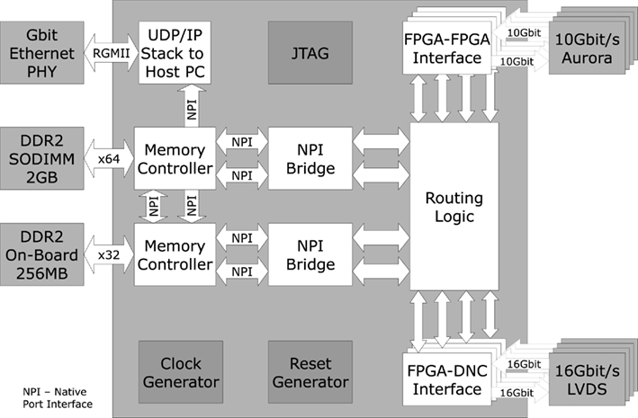
Figure 6. Block diagram of the logical FPGA structure (Hartmann et al., 2010).
The FPGA–FPGA links employ the Aurora protocol (Aurora, 2010), offering 10 Gbit/s data rate on four parallel Multi-Gigabit Transceiver lanes. Packet size on this link is 64 bit, each containing two 28 bit pulse events, i.e., event rate per FPGA–FPGA link is 312 Mevent/s. Packets sent via the FPGA–DNC link have a standard size of 128 bit, containing either four 24 bit pulse events or configuration data. This results in 500 Mevent/s maximum event rate. The link provides error detection and handling via a 9-bit CRC contained in each packet. The DNC–HICANN links employ the same 24 bit packet format for pulse events. With the offered raw data rate of 2 Gbit/s, a maximum event rate of 45.5 Mevent/s is achieved, including overhead for CRC error handling. In sum, all eight HICANN links from a single DNC offer 364 Mevent/s, matching with the 500-Mevent/s DNC–FPGA link (including overhead).
Two external memories are connected to the FPGA: A DDR2 SDRAM module with up to 4 GByte capacity is used for event storage and playback, providing high-speed stimuli or pulse recording. The module allows a maximum throughput of 742 Mevent/s for read and 589 Mevent/s for write. The second memory is a 256 MByte on-board SDRAM used for buffering of the UDP/IP host interface packets and routing tables for pulse event redirection. Memory throughput is maximized by a native port interface (NPI), supporting burst transfers.
The host communication is realized by a reduced UDP/IP hardware stack. In order to save FPGA resources, the physical layer is located on a separate chip on the PCS, which also enables the fall-back to 10/100 Mbit/s Ethernet.
The routing logic connects the FPGA–FPGA interfaces, the FPGA–DNC interfaces and the interfaces to the external memories. Pulses coming from other wafers or from the four DNCs are dispatched depending on the entries in the routing tables, stored in the routing memory. A flag in each pulse packet decides if the pulses are stored in trace memory. Additionally, new pulses are created from entries in the playback memory. In terms of resources, the maximum number of neurons to be routed to other FPGAs (i.e., other wafers) would be 16384 (equivalent to 32 HICANNs; Schemmel et al., 2010), which at 10 Hz and the speed-up factor of 104 would generate 1.64 Gevents/s. Since the on-board SDRAM offers about the same event rate for routing table lookup as mentioned above for the playback (742 Mevent/s), about 45% of those neurons could have their targets on other wafers, while the rest would have to be routed on the same wafer via the high-density routing grid (Schemmel et al., 2010). The PCS offers another option to achieve full routing of all neurons to other wafers: the routing table can be split between the on-board RAM and the RAM directly contained in the FPGA, which doubles the access rate for the routing lookup. This allows routing of almost every neuron on the wafer to another wafer. If in a worst-case scenario all neurons were to be routed to all four connected FPGAs/wafers, the total memory required would be (30 bit address) × (16384 sources) × (4 routing entries), equal to ca. 2 Mbit. This is easily within the resources offered by the Virtex 5 FPGAs employed in the PCS.
2.2.3 The integrated pulse communication subgroup
Figure 7 shows a test setup for 1 of the 12 PCSs required for a wafer module (see Figure 1). The wafer module is designed to fit into a standard 19″ rack. This limits the dimensions for each of the 12 PCSs and the associated cooling system to 92 mm × 138 mm, necessitating that the four DNC boards coupled to one FPGA be located under the FPGA board (as can be seen from the cutout in Figure 7). To save board space, an external power board delivers several power domains to the PCS which are further subdivided on their route to the DNCs. The PCS contains two Gigabit Ethernet hookups for connecting to host control, as well as four Aurora 10-GBit transceivers for inter-board (i.e., off-wafer) communication. To realize the electrical connectivity between the memories, the different interfaces and the Virtex 5 FPGA, a 14 layer PCB was designed in-house, with eight layers used for signal routing and the remaining six layers for power supply and shielding. This level of mechanical and electrical integration is significantly more advanced than commercial FPGA platforms.
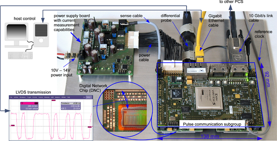
Figure 7. Photograph of the PCS in its measurement setup. Compared to the PCS in Figure 1, the heat pipes and heat sink have been removed for better visibility.
2.3 Measurement Setup
2.3.1 Communication measurement setup
The setup shown in Figure 7 can be directly used to measure the characteristics of the network connection that is realized by the DNC, i.e., the FPGA–DNC–HICANN connection. This is the main network connection on a single wafer, cf. Figure 2. Because a HICANN is not included in the setup, a loopback-connector is used instead, externally connecting the output of a DNC–HICANN link to its input. This connector emulates a connection to a HICANN via the system PCB and back. As a consequence of the setup, packets initiated in the FPGA traverse all network links and processing units of the off-wafer network.
The measurement setup is operated from the host PC, allowing to fully characterize the PCS infrastructure. This includes bandwidth tests, where throughput (see Table 1) and packet loss are directly measured. Furthermore, the connection delay of each pulse packet is monitored, enabling an assessment of the DNC’s sorting and buffering functionality.
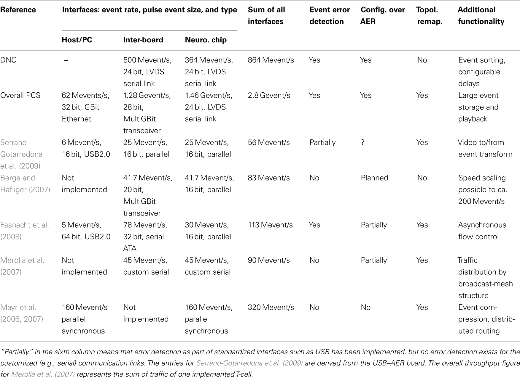
Table 1. Characteristics of the presented DNC, overall PCS, and comparable implementations.
To prevent any distortions of the measurements by the host interface, pulse packets are transmitted to the FPGA’s internal SDRAM before the measurement. Each packet is supplemented by a release timestamp, defining the time the pulse’s transmission is started at the FPGA. During the measurement, the FPGA plays back the pulse packets according to their release time. Simultaneously, it stores all incoming packets from DNCs in the SDRAM, additionally registering their receive time. From the monitored received packets and the sent packets, the measurement is analyzed in the host PC, calculating bandwidths, pulse loss, and pulse delays, as shown in the following.
2.3.2 Pulse transmission test
For compatibility with common modeling approaches (Brunel, 2000), we use Poisson spike trains for stimulation during the hardware experiments. To avoid any pulse loss during the pulse release in the FPGA, all pulses that have identical release timestamp to the preceding packet are excluded. This is because only one event packet per timestamp value (i.e., FPGA clock cycle) can be sent to a single HICANN. In normal system operation, a prioritization logic resolves any packet congestion, delaying packets if necessary. However, because we need to release all packets exactly at their FPGA release time for correct delay measurement, we did not include such a mechanism in the measurement setup.
For delay measurements, Poisson spike trains with a biological rate of 10 Hz each were generated for 64 addresses, each corresponding to a separate neuron address on the same HICANN. For evaluating the delays of individual spikes, the time differences between sent and received pulses are analyzed. Each neuron address is configured for a different nominal delay value, expressed as the difference between the FPGA release timestamp and the timestamp contained in the pulse packet. Since the pulses are only registered once they are received back in the FPGA, we subtract a constant value of 200 ns from the measured delays. This accounts for the transmission time of the return connection (loopback-DNC–FPGA), which is not included in the nominal delay realized by the DNC.
For throughput measurements, 128 independent Poisson spike sources with identical sweep of the mean rate are used. Both the low- and high-speed mode were employed for the test. The nominal delay value for all spike sources was set to 400 ns (i.e., 4 ms biological).
2.3.3 Neuromorphic benchmark test
Neuromorphic testing of the PCS beyond the communication benchmarks mentioned above is complicated by the fact that the remaining components of the waferscale neuromorphic system are currently in various stages of development, i.e., there is no fully operational waferscale setup which could be used to characterize the PCS. The accelerated nature of the system also precludes a test via a direct software/hardware coupling, i.e., a neuromorphic benchmark running in software which could employ the PCS for pulse transmission. The software simulation would simply not be fast enough to successfully interact with the hardware. However, Kremkow et al. (2010) have published a model of effective feedforward inhibition in an extended synfire chain (see Figure 8), which can be used to characterize the neuromorphic applicability of the PCS. Since the single populations of regular spiking (RS) and fast spiking (FS) neurons in Figure 8 are only connected by feedforward couplings, it is possible to simulate the populations offline in NEST (Gewaltig and Diesmann, 2007) in our test setup. The spikes emitted by an RS population are then transferred in software to the subsequent RS and FS populations, while the spikes of the inhibitory FS–RS coupling are transferred in hardware via the packet-based network of the PCS. As in Kremkow et al. (2010), we have set the delay of the RS population spikes for all tests to a fixed 20 ms, which could, however, also be set to zero as it affects the subsequent RS and FS populations at the same time and thus has no effect on the feedforward propagation.
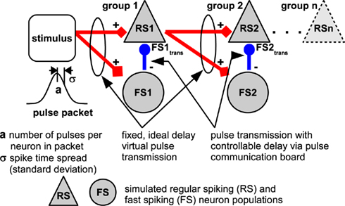
Figure 8. Model of a synfire chain with feedforward inhibition employing a controllable delay, figure adapted from Kremkow et al. (2010).
Accordingly, the software transfer of spikes would in this context be similar to the delay-less high-density routing grid on the wafer (i.e., as if the feedforward chain would be realized in neurons/synapses on the same wafer). At the same time, the configurable delay of the packet-based network can be employed to control the propagation selectivity of the feedforward network (Kremkow et al., 2010). For this test, the topology of the network, coupling strength, neuron types, and the propagation analysis are identical to Kremkow et al. (2010). Specifically, the sizes of the RS and FS populations are NRS = 100 and NFS = 25, respectively. As the parameters of the temporally fluctuating background noise current are not defined in the reference, we have exchanged it with a constant current of 29 nA for each neuron, which agrees well with the simulation results of Kremkow et al. (2010). For the DNC, the 2-Gbit/s high-speed mode is employed.
For fitting the separatrix between the transmission and suppression states (cf. Figure 13), we used the function  according to Kremkow et al. (2010). Therefore, we performed a bisectioning search for finding the exponent c3 with the minimum fitting error, explicitly calculating c2 from the minimum error condition. For ensuring reasonable fitting solutions, i.e., monotonically increasing functions, we set c1 = 0.8 in accordance with Kremkow et al. (2010).
3 Results
3.1 Communication Measurement
Figure 9A shows a typical spike sequence for stimulation and the times of received spikes during the experiment. Due to the Poisson statistics, spike trains are not regular in time, but include intervals with an increased spike rate that have to be handled by the buffering units in the DNC. The connection delays have been configured to increase with the neuron address, as can be seen in the plot.
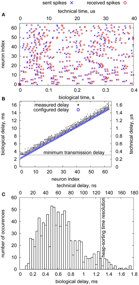
Figure 9. Delay measurement of the FPGA–DNC–HICANN connection. (A) sent/received spikes (B) measured delays (C) delay jitter.
Due to mixing of pulses with differing nominal delays at the FPGA, release times of pulses at the DNC are unsorted. Thus, without sorting and buffering, delay jitter would be high and unspecific. In contrast, with these functions included in the DNC, pulses arrive approximately at their nominal delay, as Figure 9B shows. Almost all delay values deviate less than 1.5 ms in biological time (150 ns technical time), cf. Figure 9C. The delay jitter is mainly caused by the sorting resolution of the DNC: The lower 5 bit of the timestamp are not used in time comparisons to allow for faster execution. Thus, the time resolution is 32 clock cycles, corresponding to 1.28 ms in biological time. A final buffering stage with full resolution (4 ns technical time, 0.04 ms biological time) has been included in the HICANN, which, however, is not part of the setup. Nevertheless, the achieved delay jitter is in the order of the resolution limit for biological neurons (Bohte, 2004), so that already the sorting/buffering functionality of the DNC provides biologically realistic constant-delay connections.
The minimum transmission delay of the FPGA–DNC–HICANN connection is 310 ns (3.1 ms biological time), visible in the lower left part of Figure 9B. This is caused by the inherent delays of the LVDS transmission and the packet handling in the DNC and cannot be further reduced. This delay is in the order of short-range connections in biologically realistic models of neural networks (Hill and Tononi, 2005). For long-range connections, the remaining connection links (HICANN–DNC–FPGA–FPGA) have to be taken into account. These introduce approximately 500 ns (5 ms biological time) additional delay, thus biologically realistic values of ≥8 ms for long-range connections can be configured. The upper bound for the configurable delays inherent in the timestamp is 214 × 4 ns = 65.5 μs (655 ms biological time), which is the point at which the timestamps can not be uniquely resolved anymore in the DNC. However, timestamps can be extended beyond 15 bit in the FPGA, effectively making arbitrarily long delays possible. In this case, a pre-buffering in the FPGA evaluates the additional timestamp bits and accordingly releases the event to the DNC in its original 15 bit format.
Figures 10A,B show the rate of received pulses and the pulse loss with respect to the stimulation rate. The received spike rate (throughput) saturates at approximately 90% of the maximum available rate (45.5 Mevent/s). Thus, even for rather irregular Poisson firing patterns, almost the full bandwidth can be utilized. This utilization stays constant also for higher stimulation rates, proving that the sorting/buffering unit in the DNC can handle overflows of arriving packets without degrading performance. This is despite the fact that insertion and removal time of packets increases with the buffer filling level (Scholze et al., 2010). The pulse loss naturally increases with the saturation of the throughput, as Figure 10B depicts. A small fraction of pulses is dropped also below saturation rate. This is due to bursts occurring in the spike trains. If too many spikes had to be delivered to the HICANN in a short time interval, some of them would have to be delayed in the DNC. However, this could result in some of the pulses arriving significantly later than given by their configured delay. This in turn could significantly affect network behavior, especially with spike-based learning (Izhikevich et al., 2004; Wenisch et al., 2005). Therefore, these pulses are discarded, so that no learning occurs on the HICANN instead of learning in a wrong direction (Schemmel et al., 2006).
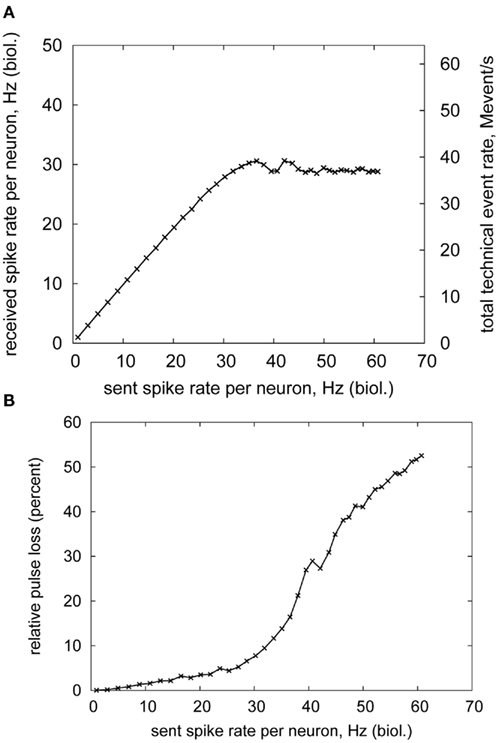
Figure 10. Bandwidth measurement of a single FPGA–DNC–HICANN connection. (A) received spike rate (B) spike loss.
3.2 Benchmark Network Measurement
For evaluating the applicability of the DNC to biologically realistic network experiments, we chose the synfire chain network by Kremkow et al. (2010). The details of the setup are described in Section 2.3.3 and shown in Figure 8: The spikes from the inhibitory neurons (FS) to the excitatory population (RS) are transmitted via the communication subgroup. These are the most performance-critical connections in the network, because their delay and reliability determines the selectivity of the whole synfire chain to the temporal spread of the stimulus.
Figure 11 shows an example of the synfire chain behavior with hardware transmission. The spikes in the chain become synchronized because the excitatory neurons are driven by similar inputs. Neurons in the inhibitory population (FS) spike earlier than those in the excitatory population (RS) due to their higher weights (Kremkow et al., 2010). If this time difference is smaller than the delay of the FS-to-RS connections, the arriving spikes suppress the activity in the RS population before its neurons can reach the spiking threshold. In contrast, Figure 11 shows an example with a relatively long delay of FS-to-RS connections. In this case, the RS population can emit one spike wave before being inhibited, which is then transmitted reliably through the chain (compare Kremkow et al., 2010).
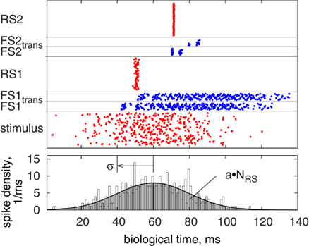
Figure 11. A sample pulse pattern of the synfire chain, with pulses of the inhibitory FS populations transmitted via the PCS. Upper plot: pulses sorted by population, from the bottom: initial stimulus, resultant activity of the first inhibitory FS population before (FS1) and after (FS1trans) transmission, activity of the first excitatory RS population (RS1), and the corresponding patterns for the second group of populations (compare Figure 8). Lower plot: given spike density and resulting histogram of the stimulus in the upper plot. Parameters are a = 4, σ = 20 ms, FS-to-RS (hardware) delay 10 ms.
Figure 11 also shows the influence of the hardware transmission: When pulses occur at the same time, some are discarded because of the serial transmission (cf. FS2trans compared to FS2). For further investigation of these transmission properties, we tested spike volleys as used in the synfire chain with different number of spikes and temporal spread, analyzing the received spike train in terms of count and temporal spread. Results of these experiments are shown in Figure 12. For most cases, no pulse loss or deviation in temporal spread occurred, meaning that the PCS’s bandwidth and buffering/delaying capabilities were sufficient. Only for a high spike count together with a low temporal spread, significant pulse loss and increased temporal spread are encountered. This constitutes the expected critical case, for which many spikes need to be transmitted in a short time over the serial LVDS channel. However, this regime is biologically unrealistic, because it does conflict with the refractoriness of biological neurons, which restricts their minimum inter-spike interval to a few milliseconds. As a result of the pulse loss, it can be expected that the synfire chain with pulse transmission via the PCS is less selective because of the reduced inhibitory effect.
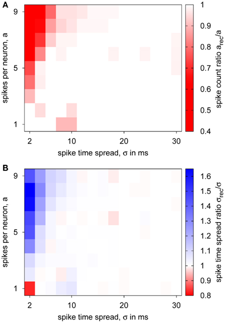
Figure 12. Transmission of spike volleys by the PCS. Pulse packets for 10 spike sources with varying number of spikes per neuron a and temporal spread σ were transmitted via the PCS, configured with an 8-ms delay, and the received spike train characterized: (A) fraction of actually transmitted pulses, (B) temporal spread ratio of received and sent pulse packets.
For characterizing the overall behavior of the synfire chain for different FS-to-RS delays, we performed the same state space sweeps as in Kremkow et al. (2010). In these simulations, the pulse count and the temporal spread of the stimulating spike volley are varied similar to Figure 12 and the principal network state (activity suppression or transmission to the last population) is monitored. Figures 13A,B show the state space diagrams with 4 ms FS-to-RS delay for ideal and hardware transmission, respectively. For small temporal spreads and high spike counts, more spike waves are persistent in the hardware transmission case compared to the ideal simulations. This is caused by the pulse loss of the hardware transmission (cf. Figure 12A) and the resulting reduction of inhibitory effectiveness. However, these deviations do only slightly affect the state boundary between transmission and activity suppression, which is summarized according to Kremkow et al. (2010) in the location of the separatrix curve, which denotes the fitted boundary.
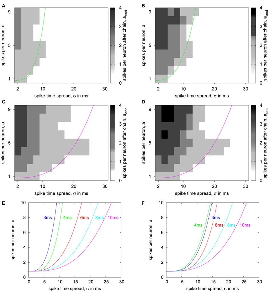
Figure 13. State space diagrams for the synfire chain. (A–D) Number of spikes per neuron in the last excitatory population of the synfire chain with respect to the parameters of the initial stimulation for ideal (A,C) and hardware (B,D) transmission and delays 4 ms (A,B) and 10 ms (C,D). The solid lines indicate the fitted separatrix between successful transmission of the spike volley to the end of the chain and diminishing activity. (E,F) Separatrices for different delay settings with ideal (E) and hardware (F) transmission.
Experiments with 10 ms FS-to-RS delay result in the same principle behavior, as depicted in Figures 13C,D: For low temporal spread, more spike waves are transmitted when using the hardware, but this does not affect the boundary of the transmission region in the state space. In the 10-ms case, a special effect in the state space diagram occurs: At an intermediate number of spikes, the transmission state extends to relatively big temporal spreads, for which the network is suppressive at higher spike count. This is caused by the amplitude of the inhibitory activity: At high temporal spreads, the RS population encounters inhibition always before its own first spiking activity. However, for intermediate spike counts, the inhibitory effect is not strong enough to suppress the first RS spike wave. In contrast, if the number of spikes in the stimulus is increased, the inhibitory activity gets strong enough to impede any spiking in the RS population. This effect is not reflected in the separatrix curve as formulated in Kremkow et al. (2010), because this constitutes only a mean, monotonically increasing boundary.
Figures 13E,F summarize the state space separatrices for a sequence of FS-to-RS delays. These confirm the good reproduction of the ideal simulated case by the simulations with hardware transmission. Only for 3 ms, the hardware case is not as selective as the ideal simulation. This result seems to conflict with the delay measurement (cf. Figure 9), where pulses with 3 ms or above were reliably transmitted. The difference between both cases is that the delay test was performed at a relatively low rate, whereas the spike trains in the synfire chain experiments constitute short, high-rate bursts. In the hardware, the temporal window for buffering diminishes when approaching the minimum transmission delay, which is approximately 3 ms. In consequence, simultaneously arriving pulses can not be delayed to transmit them serially, but some of them have to be discarded (cf. Figure 12). This results in a significantly increased pulse loss, which reduces the inhibitory activity also for parameters near the boundary in the state space, making the hardware synfire chain less selective.
3.3 Overall Characteristics
Table 1 gives a comparison with other AER system solutions. Apart from the systems described in Merolla et al. (2007) and Mayr et al. (2006), all of them are based only on FPGAs for implementing their communication protocols and neuromorphic functionality, no ASIC design was carried out. Their interfaces are either parallel asynchronous AER (Serrano-Gotarredona et al., 2009) or a variety of adapted commercial standards. In terms of speed, the systems of Berge and Häfliger (2007) and Fasnacht et al. (2008) come closest to our implementation, but are still (even for the planned speed-up of Berge and Häfliger, 2007) a factor of 4 smaller for the DNC on its own, or if the overall PCS is compared, a factor of 25. In terms of architecture, most FPGA boards are intended as a central hub/controller for all connected neuromorphic chips, in contrast to the multiple PCS instances required for a wafer. In this respect, our PCS is closer to the broadcast-mesh architecture of Merolla et al. (2007).
Regarding the single interface throughput figures in Table 1, a typical application scenario of the waferscale neuromorphic would be the following: A network model is realized across several wafers, e.g., a macrocolumn of V1, with a simulated retina feeding into the wafers via the host/PC connection. The inter-board links would provide the long distance connection in the model, i.e., the parts of the macrocolumn realized on different wafers. These two traffic streams are merged in the FPGA and transmitted via the DNCs to the wafer, so that naturally the bandwidth down to the wafer (link to the neuromorphic chip) has to be at least equal to the sum of the inter-wafer and host/PC interface.
The bandwidth per single HICANN translates into 45.5 Mevents/s (see Table 1, the entry for PCS down to neuromorphic chip divided by 32 HICANNs), which contrasts with the 51.2-Mevents/s requirement derived in Section 2.1.2. However, the estimate of Section 2.1.2 is a worst-case estimate for a fully utilized wafer and for every neuron having a connection to the outside, i.e., there are no neurons just connected intra-wafer. Thus, the achieved bandwidth should be sufficient for most experiments.
4 Discussion
A highly integrated neuromorphic pulse communication board (PCS) containing an application-specific packet-based AER communication ASIC (the DNC) has been presented. The packet-based network provides pulse stimulation and monitoring as well as control and configuration of all the circuits on the wafer via the same links. Compared to other recent solutions, the full bandwidth of high-speed serial communications covers the entire chain from PC via FPGA, DNCs down to the neuromorphic chips (HICANNs), avoiding a parallel AER bottleneck (Berge and Häfliger, 2007; Fasnacht et al., 2008). Also, the full AER bandwidth is available for configuration of the wafer. This feature is crucial since the DNC and FPGA constitute the sole interface between the wafer and the outside. As Table 1 shows, a speed increase well over an order of magnitude compared to the state of the art has been achieved. In terms of transmission integrity, compared to our PCS, all the solutions in Table 1 offer only partial or no error detection for the pulse events.
In terms of a neuromorphic application of the PCS, Figure 10 shows that the theoretical pulse communication bandwidths of Table 1 are achievable for the PCS for biologically plausible Poisson spike trains. Figure 12 extends this analysis, showing that the overall PCS characteristics (i.e., buffer sizes, throughput, etc.) are compatible with a wide range of generic neuromorphic spike traffic. The configurable pulse delays offered by the DNC timestamp sorting (see Figure 9) are in the range and precision of biological axonal/dendritic delays (Bohte, 2004; Hill and Tononi, 2005). The delay-selective signal propagation in the synfire chain model of Kremkow et al. (2010) has been employed to show that delay-based neural computation is feasible in the waferscale neuromorphic system using the packet-based AER functionality (compare Figures 13E,F). In an extension of the “separatrix”-analysis of Kremkow et al. (2010), signal propagation in the synfire chain has also been shown for cases where the initial stimulus exhibits a relatively big temporal spread at an intermediate number of spikes (see Figure 13C). This particular effect is present in both the ideal benchmark and the hardware implementation (compare Figures 13C,D) and can be easily explained in terms of fundamental network behavior. However, it is partially masked by the “separatrix”-analysis, with the separatrix curve implying that there is no pulse transmission for these parameter ranges (compare separatrix curve and actual transmission characteristic in Figure 13C).
Conflict of Interest Statement
The authors declare that the research was conducted in the absence of any commercial or financial relationships that could be construed as a potential conflict of interest.
Acknowledgments
We would thank the members of the Vision(s) group at KIP Heidelberg for fruitful collaboration on the overall design of the waferscale neuromorphic system. The research leading to these results has received funding from the European Union Seventh Framework Programme (FP7/2007-2013) under grant agreement no. 269921 (BrainScaleS).
References
ANS. (2001). Electrical Characteristics of Low Voltage Differential Signaling (LVDS) Interface Circuits, 644th Edn. [ansi/tia/eia]. http://standardsdocuments.tiaonline.org/tia-eia-644-a.htm
Aurora. (2010). Aurora 8B/10B Protocol Specification. SP002(v2.2). Xilinx, Inc. http://www.xilinx.com/support/documentation/ip_documentation/aurora_8b10b_protocol_spec_sp002.pdf
Berge, H., and Häfliger, P. (2007). “High-speed serial AER on FPGA,” in International Symposium on Circuits and Systems 2007, New Orleans, LA, 857–860.
Bohte, S. (2004). The evidence for neural information processing with precise spike-times: a survey. Nat. Comput. 3, 195–206.
Brunel, N. (2000). Dynamics of sparsely connected networks of excitatory and inhibitory spiking neurons. J. Comput. Neurosci. 8, 183–208.
Deco, G., Jirsac, V., McIntosh, A., Sporns, O., and Kötter, R. (2009). Key role of coupling, delay, and noise in resting brain fluctuations. Proc. Natl. Acad. Sci. U.S.A. 106, 10302–10307.
Ehrlich, M., Mayr, C., Eisenreich, H., Henker, S., Srowig, A., Grübl, A., Schemmel, J., and Schüffny, R. (2007). “Wafer-scale VLSI implementations of pulse coupled neural networks,” in IEEE International Conference on Sensors, Circuits and Instrumentation Systems, Hammamet.
Fasnacht, D., Whatley, A., and Indiveri, G. (2008). “A serial communication infrastructure for multi-chip address event systems,” in International Symposium on Circuits and Systems 2008, Seattle, WA, 648–651.
Giulioni, M., Camilleri, P., Dante, V., Badoni, D., Indiveri, G., Braun, J., and Del Giudice, P. (2008). “A VLSI network of spiking neurons with plastic fully configurable ‘stop-learning’ synapses,” in 15th IEEE International Conference on Electronics, Circuits and Systems, ICECS 2008, Malta, 678–681.
Hartmann, S., Schiefer, S., Scholze, S., Partzsch, J., Mayr, C., Henker, S., and Schüffny, R. (2010). “Highly integrated packet-based AER communication infrastructure with 3Gevent/s throughput,” in Proceedings of IEEE International Conference on Electronics, Circuits, and Systems ICECS10, Athens, 952–955.
Hill, S., and Tononi, G. (2005). modeling sleep and wakefulness in the thalamocortical system. J. Neurophysiol. 93, 1671–1698.
Izhikevich, E., Gally, J., and Edelman, G. (2004). Spike-timing dynamics of neuronal groups. Cereb. Cortex 14, 933–944.
Jin, X., Furber, S., and Woods, J. (2008). “Efficient modelling of spiking neural networks on a scalable chip multiprocessor,” in International Joint Conference on Neural Networks 2008, Hong Kong, 2812–2819.
Kremkow, J., Perrinet, L., Masson, G., and Aertsen, A. (2010). Functional consequences of correlated excitatory and inhibitory conductances in cortical networks. J. Comput. Neurosci. 28, 579–594.
Mayr, C., Eisenreich, H., Henker, S., and Schüffny, R. (2006). Pulsed multi-layered image filtering: a VLSI implementation. Int. J. Appl. Math. Comput. Sci. 1, 60–65.
Mayr, C., Heittmann, A., and Schüffny, R. (2007). Gabor-like image filtering using a neural microcircuit. IEEE Trans. Neural Netw. 18, 955–959.
Mehring, C., Hehl, U., Kubo, M., Diesmann, M., and Aertsen, A. (2003). Activity dynamics and propagation of synchronous spiking in locally connected random networks. Biol. Cybern. 88, 395–408.
Merolla, P., Arthur, J., Shi, B., and Boahen, K. (2007). Expandable networks for neuromorphic chips. IEEE Trans. Circuits Syst. I Regul. Pap. 54, 301–311.
Meyer, U., Shao, J., Chakrabarty, S., Brandt, S., Luksch, H., and Wessel, R. (2008). Distributed delays stabilize neural feedback systems. Biol. Cybern. 99, 79–87.
Partzsch, J., and Schüffny, R. (2011). Analyzing the scaling of connectivity in neuromorphic hardware and in models of neural networks. IEEE Trans. Neural Netw. 22, 919–935.
Schemmel, J., Brüderle, D., Grübl, A., Hock, M., Meier, K., and Millner, S. (2010). “A wafer-scale neuromorphic hardware system for large-scale neural modeling,” in International Symposium on Circuits and Systems 2010, Paris, 1947–1950.
Schemmel, J., Grübl, A., Meier, K., and Mueller, E. (2006). “Implementing synaptic plasticity in a VLSI spiking neural network model,” in International Joint Conference on Neural Networks IJCNN ’06, Vancouver, BC, 1–6.
Scholze, S., Eisenreich, H., Höppner, S., Ellguth, G., Henker, S., Ander, M., Hänzsche, S., Partzsch, J., Mayr, C., and Schüffny, R. (2011). A 32 GBit/s communication SoC for a waferscale neuromorphic system. Integr. VLSI J. http://dx.doi.org/10.1016/j.vlsi.2011.05.003
Scholze, S., Henker, S., Partzsch, J., Mayr, C., and Schüffny, R. (2010). “Optimized queue based communication in VLSI using a weakly ordered binary heap,” in Mixed Design of Integrated Circuits and Systems 2010, Wroclaw, 316–320.
Serrano-Gotarredona, R., Oster, M., Lichtsteiner, P., Linares-Barranco, A., and Paz-Vicente, Rea. (2009). CAVIAR: a 45k neuron, 5M synapse, 12G connects/s AER hardware sensory-processing-learning-actuating system for high-speed visual object recognition and tracking. IEEE Trans. Neural Netw. 20, 1417–1434.
Keywords: serial AER in VLSI, packet-based AER, configuration over AER, configurable pulse delays
Citation: Scholze S, Schiefer S, Partzsch J, Hartmann S, Mayr CG, Hoppner S, Eisenreich H, Henker S, Vogginger B and Schuffny R (2011) VLSI implementation of a 2.8 Gevent/s packet-based AER interface with routing and event sorting functionality. Front. Neurosci. 5:117. doi: 10.3389/fnins.2011.00117
Received: 12 July 2011; Accepted: 14 September 2011;
Published online: 12 October 2011.
Edited by:
Chiara Bartolozzi, Italian Institute of Technology, ItalyReviewed by:
Alejandro Linares-Barranco, University of Seville, SpainSrinjoy Mitra, Inter University Microelectronics Centre, Belgium
Daniel Bernhard Fasnacht, Institute of Neuroinformatics, Switzerland
Copyright: © 2011 Scholze, Schiefer, Partzsch, Hartmann, Mayr, Höppner, Eisenreich, Henker, Vogginger and Schüffny. This is an open-access article subject to a non-exclusive license between the authors and Frontiers Media SA, which permits use, distribution and reproduction in other forums, provided the original authors and source are credited and other Frontiers conditions are complied with.
*Correspondence: Christian Georg Mayr, Chair of Highly-Parallel VLSI-Systems and Neuromorphic Circuits, Institute of Circuits and Systems, Technische Universität Dresden, 01062 Dresden, Germany. e-mail:bWF5ckBpZWUuZXQudHUtZHJlc2Rlbi5kZQ==