 Corentin Delacour
 Aida Todri-Sanial
- Laboratoire d'Informatique, de Robotique et de Microélectronique de Montpellier, Département de Microélectronique, Université de Montpellier, CNRS, Montpellier, France
Oscillatory Neural Network (ONN) is an emerging neuromorphic architecture with oscillators representing neurons and information encoded in oscillator's phase relations. In an ONN, oscillators are coupled with electrical elements to define the network's weights and achieve massive parallel computation. As the weights preserve the network functionality, mapping weights to coupling elements plays a crucial role in ONN performance. In this work, we investigate relaxation oscillators based on VO2 material, and we propose a methodology to map Hebbian coefficients to ONN coupling resistances, allowing a large-scale ONN design. We develop an analytical framework to map weight coefficients into coupling resistor values to analyze ONN architecture performance. We report on an ONN with 60 fully-connected oscillators that perform pattern recognition as a Hopfield Neural Network.
1. Introduction
Coupled oscillators have been studied for decades by scientists to describe natural phenomena (Winfree, 1967) such as the synchronization of pacemaker cells responsible for the heart beating, the synchronous behavior of insect populations, or to model neuronal activity. For instance, oscillator interactions have been shown to describe memory mechanisms and other cognitive processes in the brain (Fell and Axmacher, 2011). To characterize this variety of natural oscillations, several mathematical models (Acebrón et al., 2005; Izhikevich and Kuramoto, 2006) have been developed to explain the synchronization and phase relations in groups of coupled oscillators. Meanwhile, their massive parallel computing capability has been proved by Hoppensteadt and Izhikevich (2000), Vassilieva et al. (2011), and Parihar et al. (2017) and has raised interest in designing ONN as hardware accelerators for Artificial Neural Networks (ANN) by encoding neurons' activation in the phase between oscillators. Different types of ONN have since been developed using PLLs (Hoppensteadt and Izhikevich, 2000) or oscillators in CMOS technology (Maffezzoni et al., 2015a, 2016; Jackson et al., 2018), demonstrating pattern recognition or resolution of some optimization problems like the Traveling-Salesman-Problem (Endo and Takeyama, 1992). However, to design a competitive ONN at a large scale, a design framework is needed to establish a formalism on how to perform computations with ONN and also compare its energy efficiency with ANNs running on digital processors.
Researchers have developed oscillators by using non-linear devices such as spin-torque-oscillators (Raychowdhury et al., 2019) or with materials presenting a hysteresis resistive state to induce electrical oscillations when properly biased (Sharma et al., 2015; Wang et al., 2017). A compact device that transitions from metallic to insulating state (MIT) can be manufactured with vanadium dioxide (VO2) (Corti et al., 2018), and has recently become an interesting candidate to design energy-efficient relaxation oscillators. Moreover, coupled-VO2-based oscillators have been experimentally validated for various applications such as image saliency detection (Shukla et al., 2014), graph coloring (Parihar et al., 2017), filters in Convolutional Neural Networks (Corti et al., 2021) and implementing Hopfield Neural Networks (HNN) for pattern recognition (Corti et al., 2020).
In an HNN defined by Hopfield (1982), every neuron is connected to all the others, and synaptic weights are computed with the Hebbian rule (Hoppensteadt and Izhikevich, 2000). However, setting the right coupling element between oscillators in ONNs remains a challenge (Todri-Sanial et al., 2021). Given N fully-coupled VO2-oscillators, it is yet unknown how to transform the coefficients obtained analytically via the Hebbian learning rule to coupling resistor values among oscillators. Further, how can one interpret the coefficient signs Wij such as positive or negative values?
For weakly coupled oscillators with sinusoidal waveform, one can use the models that exist in literature (Izhikevich and Kuramoto, 2006; Maffezzoni et al., 2016) for synaptic design. However, it is more difficult for non-linear relaxation oscillators as there is no direct mapping between models and hardware. Two VO2-oscillators coupled by a capacitance or a resistance have been studied (Maffezzoni et al., 2015b; Parihar et al., 2015), but to the best of our knowledge, there is not yet a formalism to map weights to coupling elements in a larger network. This formalism is a crucial step to allow large-scale ONN design exploration. A greedy approach would be to tune the coupling elements corresponding to the most negative and most positive weights and linearly interpolate all the other weight values. However, this would be impractical. It would require repeated simulations and re-tuning coupling resistances when changing any oscillator parameter; hence, it is not suitable for large-scale ONN design. Parihar et al. (2015) proposed to use capacitors or resistors to implement a negative or a positive weight, respectively. However, it would imply using twice as many components to emulate a complete signed synaptic range.
In this work, we propose a mathematical framework to map both negative and positive Hebbian coefficient values to ONN coupling resistances, as illustrated on Figure 1. We first present a single VO2-oscillator followed by the dynamics of two coupled oscillators. Then, we show that adding switches between oscillators and coupling elements enhances the ONN dynamics control. Based on this simple architecture, we present the ONN computation style and how coupling resistances set the ONN memory expressed in different phase states. Next, by merging oscillators' dynamics with HNN formalism, we introduce the ONN mapping function that maps Hebbian coefficient values to coupling resistance values. Finally, we report on the architecture and mapping results by simulating 60 coupled VO2-oscillators for pattern recognition.
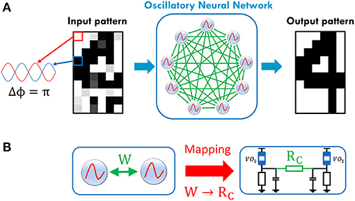
Figure 1. (A) Illustration of ONN as a Hopfield Neural Network (HNN). HNN binary activations are translated in the phase relation between oscillators and a reference (here the first oscillator). ONN stores patterns via weights between the oscillators. Patterns can be retrieved if the input pattern is sufficiently close to the stored pattern. (B) The proposed mapping function to map any weight to a coupling resistance, facilitating large scale ONN design.
2. Materials and Methods
2.1. Description of the ONN Building Blocks
2.1.1. General Properties
Unlike most ANNs where signals of interest are amplitudes, ONN consists of N VO2-oscillators coupled by resistances where the final result is given by N-1 phase relations to a reference oscillator (Corti et al., 2018). Despite this difference, there are several aspects common to any ANN that motivate our ONN study:
• The network is composed of neurons (oscillators) having input and output nodes.
• The activation function between the oscillator input and output is non-linear. For more than two oscillators, the activation function is unknown but bounded as the output phase difference of neuron i is in the range [0;180°].
• ONN has a memory (coupling resistances) and can therefore be trained to achieve specific functionality.
We use these properties to implement an HNN (Hopfield, 1982) by encoding its binary outputs in the ONN phase as shown in Figure 1A. Conveniently, we can represent each oscillator's output as a black pixel if or as a white pixel if .
2.1.2. VO2 Device
Vanadium dioxide is a material which presents temperature-driven phase change transitions. At room temperature, it remains semiconductor (insulating state) with a monoclinic crystal structure and transitions to a rutile metallic state when the temperature reaches a threshold (Corti et al., 2021). VO2 presents an hysteresis behavior as it needs to reach a lower temperature threshold to transition back to the insulating state (Figure 2A).
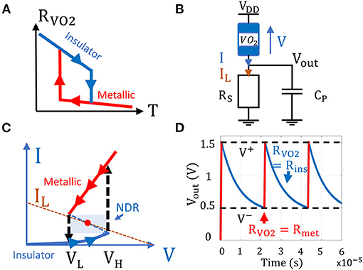
Figure 2. (A) VO2 resistance vs. temperature. RVO2 axis is in logarithmic scale. (B) VO2 oscillator circuit (C) VO2 I-V curve showing the device hysteresis behavior. When its voltage reaches a threshold VH, it transitions from insulating to the metallic state. To transition from a metallic to insulating state, V must be lower than the threshold VL. (D) If the device is biased in its Negative Differential Resistance region (NDR), its state alternates between the metallic and insulating state, producing electrical oscillations.
When a VO2 device is in series with a biasing load (Figure 2B), the voltage drop V across the device induces Joule heating which can trigger the insulating to metallic transition (IMT). To obtain the VO2 IV characteristic, we sweep the supply voltage which triggers IMT and MIT when V ≥ VH and V ≤ VL, respectively. The VO2 hysteresis behavior appears in the IV characteristic with a typical Negative Differential Region (NDR) suitable to bias the device and produce oscillations (Figure 2C).
In this work, we use the VO2 compact model from Maffezzoni et al. (2015b) which reproduces the VO2 hysteresis along with continuous and abrupt transitions between the two states. The VO2 hysteresis behavior is conceptually emulated by an amplifier with positive feedback that charges or discharges a RC circuit when the VO2 is in metallic or insulating state, respectively. The voltage Vc across the capacitor commands the VO2 conductance GVO2 as:
Where Rins and Rmet are the VO2 resistances in insulating and metallic state, respectively. The dynamics of the VO2 conductance is given by the RC circuit where τ0 is its time constant modeling the transition time of the VO2:
V0(t) is the output of the positive feedback amplifier (gain α) and is expressed as:
2.1.3. VO2 Oscillator Circuit and Dynamics
We bias the VO2 device with a series resistor RS to obtain a compact relaxation oscillator. To produce oscillations, the load line IL set by VDD and RS must intercept the VO2 I-V curve in its NDR to obtain an unstable fixed point (Figure 2C). The VO2 device state hence alternates between the metallic and insulating state. When the VO2 device is in the insulating state, the parallel capacitance CP at the output node discharges through RS until the VO2 voltage reaches VH and transitions to the metallic state. Then, CP charges through the VO2 device until its voltage reaches VL and a new cycle begins (Figure 2D).
We use circuit parameters depicted in Table 1. In this case, the load resistance RS is 20 times larger than the VO2 metallic resistance Rmet; thus, the capacitance charge time is much faster than its discharge (Figure 2D).
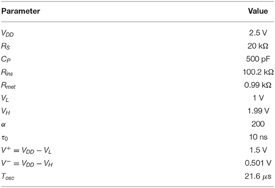
Table 1. List of parameters used for simulations in this work.
Oscillator's dynamics can be described by Kirchoff's law as:
Note that despite the first order differential equation, oscillations can occur as Equations (1–3) describe the hysteresis behavior of GVO2(t). To solve the oscillator dynamics, we start from an initial insulating VO2 state and solve numerically on Matlab the system of Equations (1–4) by using Euler's method and Newton-Raphson's algorithm for non-linear Equation (3). Figure 2D shows an example where Vout(t = 0) = 0V, GVO2(t = 0) = 1/Rins, and VDD(t = 0) = 2.5V.
2.1.4. Initialization of Two Coupled Oscillators
Two coupled oscillators represent the smallest ONN and serve as the building block for large-scale ONN. To provide input to the ONN, we delay the second oscillator VDD starting time with respect to the first oscillator (reference oscillator) to set an initial phase relation between them. Assuming oscillators have the same period Tosc, we can translate the input delay Δtinit as an initial phase relation as:
However, if the two oscillators are always connected, they might have different oscillation periods during initialization. Therefore, their initial phase relation cannot be represented as a proportion of Tosc (5). For example, as shown in Figure 3A, the second oscillator starts Δtinit = 0.5Tosc after the first one to set an initial phase relation Δϕinit = π. For t < Δtinit, the second oscillator is off, and its output node is floating. Therefore, during this time, the equivalent load resistance of the first oscillator is RS//RC, which induces a shorter period of oscillation and hence no control on the initial phase.
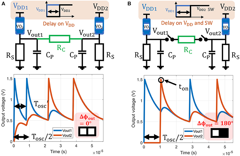
Figure 3. (A) Two oscillators are coupled by a resistance RC=10 kΩ without coupling switches in between. VDD2 is turned-on 0.5Tosc after VDD1 to set an initial phase of 180°. However, for t < 0.5Tosc the first oscillator period is decreased due to the shunt RC at its output node, and we cannot control the initial phase difference. The two oscillators are in-phase after convergence. (B) Two oscillators coupled with resistance RC=10 kΩ and coupling switches between isolate the oscillators during initialization. This time, the 0.5Tosc input delay sets desired 180° initial phase state. Here, the switches are closed at ton = 0.5Tosc + tc such that . The two oscillators converge to an 180° phase state relation.
We introduce switches between each oscillator and coupling elements as in Figure 3B to tackle this lack of control. We let each oscillator switch freely with a known oscillation period Tosc before coupling them at ton. Their dynamics can be expressed by Equation (4) and the initial conditions will be known at ton. ONN initialization is improved at the cost of one additional switch per oscillator, which can be achieved with a transfer gate.
2.1.5. Dynamics of Two Coupled Oscillators
To predict the output phases and demonstrate ONN ability to store information, we express the dynamics of the two coupled oscillators using Kirchhoff's laws:
Currents are Ic1 = −Ic2 representing the coupling element's current flow. As for the single oscillator case, we numerically solve (Equation 6) along with VO2 (Equations 1–3). Figure 4 shows a simulation where VDD2 is turned on 0.1Tosc after VDD1 which initializes a light-gray pixel for oscillator 2 input image. For a small coupling resistance, RC=10 kΩ, ONN converges to a stable state with both oscillators in-phase (0°,0°). Whereas, for RC=100 kΩ, ONN converges to out-of-phase (0°,180°). In the next subsection, we study the role of RC on ONN memory and investigate how to retrieve a stored pattern by applying an input delay Δtinit. This formulation is the core of our proposed mapping function to translate Hebbian coefficients to ONN coupling resistances.
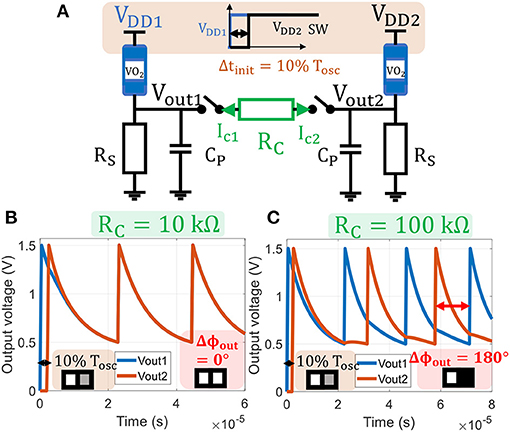
Figure 4. (A) Two identical VO2 oscillators are coupled with a resistance RC and switches. VDD2 starting time and coupling time ton are delayed by 0.1Tosc with respect to the first oscillator, representing a light-gray second pixel as ONN input. (B) Output voltages for RC = 10kΩ: the oscillators converge to an in phase state (0°, 0°) and the corresponding output pattern corresponds to two white pixels. (C) Output voltages for RC = 100kΩ: the oscillators are out-of-phase (0°, 180°) and the output pattern corresponds to a white and a black pixels.
2.1.6. Memory of Two Coupled Oscillators
We solve numerically (6) and extract the output phase relation between oscillators. Figure 5A shows the simulation results. As already observed by Corti et al. (2018), a large coupling resistance RC > 40 kΩ induces oscillators in out-of-phase relation (0°, 180°) for any input delay, whereas a small coupling resistance RC < 10kΩ aligns oscillators in-phase (0°, 0°) for any input delay.
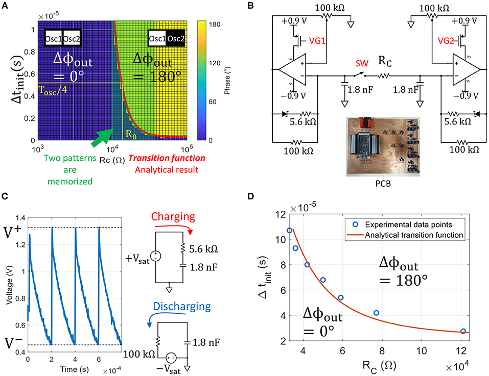
Figure 5. (A) Plot showing the phase relation between two oscillators for every set of parameters (RC, Δtinit). As expected, small coupling resistances tend to pull the oscillator phase together, whereas large coupling resistances push the phase away. The green region shows the coupling resistance range 10kΩ < RC < 40kΩ in which two patterns (0° and 0°) and (0° and 180°) are memorized and can be retrieved by adjusting the input delay. The red curve is our analytical model describing the transition between the two phase states in the plan (RC, Δtinit), and plays a major role in the ONN ability to memorize patterns. (B) Experimental set-up of two coupled relaxation oscillators based on MCP6001 OPAs. We delay VG2 with respect to VG1 by Δtinit to set the initial phase, and we close SW after initialization. (C) Experimental oscillating waveform and equivalent circuits during charge and discharge of the output capacitor. (D) Experimental phase transition curve and analytical model in plain line.
In contrast, we examine the region between these two ranges, highlighted in the center of Figure 5A. We observe that for 10kΩ ≤ RC ≤ 40kΩ both states co-exist and oscillators store two patterns (0°, 0°) and (0°, 180°) that can be retrieved by adjusting the input delay. The line transition function between in-phase and out-of-phase regions represents our analytical function for ONN memory with respect to coupling resistance and initialization. It is defined as:
With Δttransit the initial delay such that:
To confirm the existence of ζ(RC), we emulate VO2 oscillators with off-the-shelf components on a Printed Circuit Board (PCB) and we reproduce the experiment of two coupled oscillators. The relaxation oscillator circuit consists of an inverting Schmitt trigger (Schmitt, 1938) Operational Amplifier (OPA) that implements the VO2 hysteresis behavior (Figure 5B). The OPA saturates to +Vsat and −Vsat while the 1.8 nF output capacitor charges and discharges, respectively. Figure 5C shows the voltage across the output capacitor for a decoupled oscillator. Similarly to a VO2 oscillator, the OPA transitions to another state when the voltage across the output capacitor reaches V+ or V−. The 5.6 kΩ resistor implements the metallic VO2 resistance, whereas the 100 kΩ resistor corresponds to the load RS. For a fixed oscillating period of Tosc=200 μs, we vary RC and we measure Δttransit values that define the experimental transition function ζ(RC) (Figure 5D). There is a good match between experimental ζ(RC) data points and the analytical transition function derived in next subsection. Such formulation ζ(RC) is of interest as it represents a closed-form representation of ONN memory instead of repeating numerical simulations for different oscillator parameters.
2.1.7. Phase Transition Function for Two Coupled Oscillators
The phase transition function has already been observed (Nez et al., 2021) but to the best of our knowledge, no closed-form expression has ever been reported. To obtain the transition function, we solve node voltage equations analytically for two coupled oscillators during initialization (see Supplementary Material). We derive oscillator outputs as:
and are the initial voltages when oscillators are coupled and τ′ is defined in Supplementary Material Equation (S18). Equation (9) describes both oscillator output voltages attracted via the coupling resistance RC. If the coupling is strong enough (small RC), both oscillators are rapidly pulled together with a speed determined by τ′. If ΔV < ϵ (ϵ defined in Supplementary Material Equation S22) before reaching the VO2 threshold V−, then both oscillators will transition to low resistive states, and the exponential term in Equation (9) will keep the two voltages locked. This concept is illustrated in Figure 6A when both oscillators are in-phase. However, if Vout1 reaches V− before Vout2 such that ΔV > ϵ as in Figure 6B, the first oscillator transitions to a low resistance state (metallic state) while the other oscillator is still in high resistance state (insulating state). The two oscillators are then in opposite states, and this leads to out-of-phase relation.
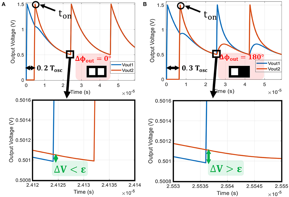
Figure 6. Two identical oscillators coupled by RC = 12kΩ. (A) The second oscillator is turned on at 0.2 Tosc after the first one. By zooming on the waveform when the first oscillator reaches V−, we observe a voltage difference ΔV < ϵ. Therefore, the oscillators converge to an in-phase state. (B) The second oscillator is turned-on 0.3 Tosc after the first one. In this case, we observe a voltage difference ΔV > ϵ and the oscillators converge to an out-of-phase state.
Thus, to obtain the transition function ζ (Equation 7), we study the case when both ΔV = ϵ and conditions are fulfilled (see Supplementary Material for details). By combining (Equations S17, S24, and S25 in Supplementary Material) we derive coupling resistance as:
where is defined in Supplementary Material Equation (S5). Finally, we introduce (Equation S9 in Supplementary Material) into Equation (10), and obtain a relation between RC and Δttransit. Note that ϵ is a function of RC, thus we cannot solve (10) analytically. Instead, we numerically solve (Equation 10) using Newton-Raphson's algorithm for Δttransit values. We finally obtain RC values that describe the inverse of the transition function as:
Transition function ζ is plotted as the curve line (red line) in Figure 5A, and there is an excellent fit between our analytical model, simulations (transition region between dark and light green in (RC, Δtinit) plan) and the transition curve obtained experimentally with off-the-shelf relaxation oscillators (Figure 5D). In addition, we can now extract the coupling resistor R0 that corresponds to a neutral synaptic connection W = 0. As by definition, both output phase states can equally occur for W = 0, we extract R0 as:
Finally, based on the transition function, we predict the final phase relation as:
Analogous to ANNs, Equation (13) can be thought of as oscillator's activation function. Because, it provides the oscillator's output phase based on its input phase (set by Δtinit; Equation 5) and the weight implemented by RC.
2.1.8. Impact of VO2 Parameters Variations on the Phase Transition Function
Fabricating reliable VO2 devices is challenging (Corti et al., 2019) and ONN experiments with VO2 are currently limited to few devices because of device variability (Shukla et al., 2016). Here, we study the impact of VO2 variability on the ability to phase-lock and on the synaptic range. The transition function ζ(RC) defines the boundary between two phase regions, and allows direct identification of the neutral coupling resistor R0 corresponding to the weight W = 0 (Equation 12). Thus, we use ζ and R0 as metrics to assess the impact of VO2 parameters' variations. We apply relative variations on VO2 parameters one at a time from –20% up to +20%, as shown in Figure 7A. Note that we vary VH from –4% up to +4% only, as for larger positive variations oscillations do not occur (load line crosses the insulating branch and forms a fixed point). For all cases, we discretize the whole input space (RC, Δtinit) and perform multiples transient simulations to extract the new phase regions. Then, we numerically solve (Equation 10) with the new sets of parameters and we verify that the transition function ζ matches the phases boundary obtained via transient simulations, as in Figure 5A.
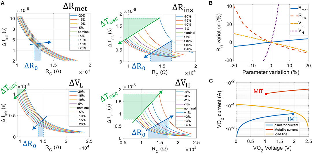
Figure 7. (A) Phase transition curves ζ(RC) when varying VO2 parameters Rmet, Rins, VL from –20 to +20%, and VH from –4 to +4% for circuit parameters listed in Table 1. Left hand side of the transition curve corresponds to inputs (Δtinit, RC) inducing whereas right hand side corresponds to phase region. VH and Rins variations correspond to IMT point variations and have the most detrimental impact on the transition function variations. The oscillating period almost doubles due to IMT variations. (B) Variations of the neutral synaptic resistance R0 with respect to VO2 parameters' variations. R0 is very sensitive to VH as –4 and +4% VH variations induce –20 and +40% R0 variations, respectively. (C) The ONN sensitivity to IMT point is mainly due to the load line IL = (VDD−V)/RS placed close to IMT point. Any IMT variation greatly impacts the oscillators' dynamics defined by CPdV/dt = IL−I.
Figure 7A shows the set of phase transition curves obtained when varying Rmet, Rins, VL and VH. Note that our current formalism assumes matched oscillators and hence, variations are applied to both coupled oscillators. For all curves, the maximum Δtinit value corresponds to an input delay of Tosc/2 and shows the oscillation period variation (highlighted in green in Figure 7A). Finally, we extract R0 for each configuration (Figure 7B). We observe that variations on the IMT point (defined by Rins and VH) induce the largest Tosc and R0 variations. With our biasing set by RS and VDD (Table 1), the most sensitive VO2 parameter is VH as +4 and –4% VH variations induces +40 and –20% R0 variations, respectively. As the dynamic of the voltage V across the VO2 device is given by CPdV/dt = IL−I, we believe this sensitivity is mainly due to the load line that passes very close to the IMT point on the VO2 IV characteristic (Figure 7C). In this case near IMT, IL(VH)−I(VH) is small and the voltage “slows down” and is very sensitive to any IMT variation. When applying –4% up to +4% VH variations, the oscillating period Tosc almost doubles (same remark with –20 and +20% Rins variations). Ideally, we would then place the load line at equal distances between MIT and IMT points (I(VL) − IL(VL) ≈ IL(VH) − I(VH)) to homogenize the impact of VO2 variations. However, we show in the next subsection that such biasing would prevent binary phase locking and that resistively coupled oscillators need a very asymmetric waveform to phase-lock to 180°.
2.1.9. Impact of Oscillators' Waveform Shape on ONN Phase-Locking
Oscillators' circuit parameters listed in Table 1 influence the oscillating frequency, amplitude and waveform shape. The oscillating waveform shape has a major influence on ONN phase-locking capability and has been studied for PLL-based ONNs by Hoppensteadt and Izhikevich (2000). Here, we study the impact of the oscillating waveform shape on the capability for pairs of oscillators to lock to the 180° phase state. We characterize the oscillating waveform shape with the ratio τd/τc, where τd and τc are the discharging and charging time constant, respectively (defined in Supplementary Material Equations S6, S7). Our transition function ζ links ONN phase-locking properties to the metric τd/τc, as ζ only depends on oscillators' internal parameters.
We reproduce the previous simulation with two coupled oscillators to extract the output phase regions for different load resistances RS that set τd/τc (Figure 8A). Note that we also could have varied VO2 parameters such as Rmet, but instead we consider the same device. For τd/τc = 3.7 (RS = 3 kΩ), we observe that the two oscillators cannot lock to for small Δtinit values. In other words, the phase state stored by a large RC cannot be fully recovered. This can be an issue for some pairs of oscillators that need an out-of-phase relationship for any input delay.
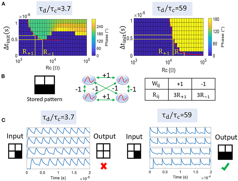
Figure 8. (A) Phase plots showing Δϕout with respect to Δtinit and coupling resistance RC between two oscillators. For τd/τc = 3.7, 180° phase state is not reachable for low Δtinit values. In contrast for τd/τc = 59, 180° phase-locking can occur for any Δtinit value for large RC. The red line is our analytical model ζ(RC) and captures well the boundary between phase regions. (B) Four coupled oscillators store a pattern composed of 2 white and 2 black pixels. Positive and negative weights are mapped to 3xR+1 and 3xR−1, respectively. (C) ONN inference for τd/τc = 3.7 and τd/τc = 59. The first configuration leads to a wrong in-phase relationship for all oscillators. In the latter case, ONN retrieves the correct stored pattern.
If τd/τc = 59 (RS = 20 kΩ), the charging time is much smaller than the discharging time and the oscillating waveform becomes very asymmetrical. Interestingly, this configuration enlarges the 180° phase region and is reachable for any Δtinit value for large RC. Our analytical model ζ(RC) predicts the correct boundary between the two phase regions (red plain lines in Figure 8A).
We study a simple case where 4 VO2-oscillators are coupled by resistances to store a single pattern (Figure 8B). Based on transition functions obtained for 2 coupled oscillators, we compute coupling resistances R+1 and R−1 that correspond to synaptic coefficients +1 and –1, respectively. We set R+1 and R−1 around R0 as and , respectively. Then, we scale coupling resistances as 3xR+1 and 3xR−1 as every oscillator is connected to 3 others (Figure 8B). We notice that ONN with τd/τc = 59 retrieves the correct stored pattern whereas ONN with τd/τc = 3.7 produces a wrong output (Figure 8C). In the latter case, we observe that all oscillators converge to an in-phase relationship. We believe this wrong behavior is mainly due to the small τd/τc value for which it is less likely ONN converges to , as described by the transition function ζ.
Figure 9 shows results of the same experiment for τd/τc varied from 1.8 up to 59 (obtained for 2 kΩ ≤ RS ≤ 20 kΩ). We observe that τd/τc > 20 is required to retrieve the correct pattern. Interestingly for τd/τc ≤ 20, there are cases where the fourth oscillator locks to a phase state around 270°. 270° phase value is also obtained in the phase plot between two coupled oscillators, such as on the left-hand side of Figure 8A. This phenomenon would allow more than two phase values but is not captured by our current formalism. In contrast, we set τd/τc to high values (59 in this work) to ensure binary 0° and 180° phase locking.
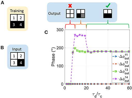
Figure 9. (A) Training pattern stored by the ONN. (B) ONN input pattern. (C) Output phase with respect to τd/τc. For τd/τc < 7, all oscillators converge to a wrong in-phase relationship. For 7 ≤ τd/τc < 20, the fourth oscillator locks to a 270° phase state. A very asymmetrical waveform such that τd/τc ≥ 20 leads to a correct binary phase-locking.
To implement a large-scale neural network such as HNN with an ONN, we need a systematic approach to map the weights to ONN coupling resistances. In the next section, we exploit some HNN features and our knowledge of two coupled oscillators to propose a mapping function.
2.2. ONN Weight Mapping
2.2.1. Applying HNN Formalism to ONN
We exploit HNN formalism to build an analogous representation in ONN. For equivalence, we treat HNN neurons similar to ONN oscillators. Such as, we consider a neuron i with two possible states Si that can be thought of as equivalent to ONN oscillators with 0° or 180° phase relations as:
In HNN, each neuron output state is dynamically determined by a sigmoid activation function g(x) = (tanh(βx) + 1)/2 (with β a positive parameter) (Gerstner et al., 2014) and shown in Figure 10. For a neuron i, g gives the probability to reach one of the two states at t + Δt for a given input weighted sum hi(t) as
with
In ONNs, Equation (15) would represent the probability of oscillator i to be in-phase with the reference at time-step Δt. For two oscillators case, the weighted input sum of the second oscillator is given by:
Then, the probability of the second oscillator to be in-phase with the reference can be derived by Equations (15) and (17), as:
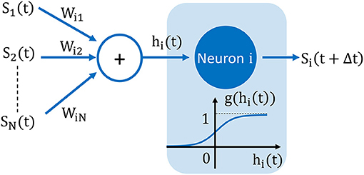
Figure 10. Model of artificial neuron used to construct our mapping function μN. The neuron's output state Si(t) is either +1 or –1 and is dynamically updated at each time-step Δt according to the sigmoid activation function g. Here, g gives the probability to have one of the two states at t + Δt for a given input weighted sum hi(t).
2.2.2. Mapping Function
Here, we apply the above definitions to derive a mapping function using the HNN formalism, as:
where, normalized weights are −1 ≤ Wij ≤ 1 and N is ONN size. Before scaling to N oscillators, we derive a mapping function μ2 for two coupled oscillators. The unifying step between HNN and ONN is the recasting of the phase transition curve, ζ as the probability Pinphase for a given coupling resistance RC. In ONNs, the input delay Δtinit can be considered as a uniform random variable taking values between 0 and Tosc/2 and the transition function ζ would give the probability Pinphase (for example for RC > 10kΩ):
and by Equations (18) and (20), we finally obtain
This mapping function is represented in Figure 11 for three different values of the sigmoid parameter, β. We see that this parameter sets the range of RC and could be adapted for different ONN sizes. Interestingly, we notice that |ΔW21/ΔRC| is quite large for a positive weight, whereas it is much smaller for a negative one. For example, we see in Figure 11B that the function ζ−1 is a logarithmic function; thus, any small variation in ΔRC around 10kΩ is likely to change the final phase state outcome. Whereas, for large RC, the two oscillators are almost always out-of-phase. This asymmetry in ζ−1 comes from the oscillator waveform type, as ζ−1 is derived from Equation (10), which is specific for relaxation oscillator waveform type. Hence, we expect some change for other types of waveforms, such as linear sawtooth, but the formulation of mapping (21) is general enough to be applied to any relaxation oscillators.
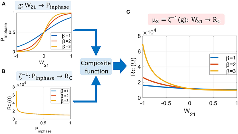
Figure 11. Mapping function for two coupled oscillators. (A) Sigmoid activation function presents the probability Pinphase for the two oscillators to be in phase. (B) Inverse of the transition function ζ−1 determines the coupling resistance RC for a given probability Pinphase. (C) The mapping function μ2 is obtained by the composite function ζ−1(g).
For large-scale ONN with N oscillators, we scale μ2 (21) by a factor N−1 to ensure the conservation of the current flow in coupling resistances. We finally obtain:
In next section, we demonstrate the effectiveness of the proposed mapping function (22) to design a 60-ONN architecture for pattern recognition as in HNN.
3. Results
3.1. ONN Design for Pattern Recognition
3.1.1. ONN Training and Mapping
In the previous section, we presented the memory capability of two coupled oscillators. Here, we apply the analytical formulas to a larger ONN size. We develop a design flow as shown in Figure 12A for pattern recognition with ONNs where we have implemented the proposed mapping function. We first compute the weights associated with the M stored patterns using the Hebbian Rule (Hoppensteadt and Izhikevich, 2000), as:
We store M = 6 images representing digits “0”, “1” to “5” as shown in Figure 12B. Next, we use our mapping function to compute the coupling resistances associated with the Hebbian coefficients. The mapping is represented in Figure 12C for different values of parameter β which sets the slope of μN(Wij). Increasing β induces a larger coupling resistance range. Because the Hebbian rule normalizes the weights by the network's size N (23), we scale β with N to keep a relative standard deviation of Rij approximately constant when increasing the ONN size. By simulations, we found that the best accuracy is obtained for β = N/32, and we report the results in subsection 3.1.3.
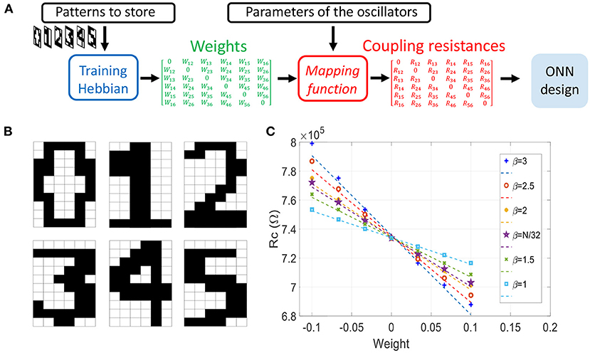
Figure 12. (A) Illustration of the ONN design flow for the associative memory application. Patterns to store can be represented as black and white images from which we compute weights with the Hebbian rule during the training process. Then, we use the mapping function μN to get the coupling resistances, allowing a systematic ONN design. (B) Stored patterns. (C) Coupling resistances as a function of Hebbian weights, computed with the mapping function μN for different values of parameter β.
3.1.2. ONN Inference
For every input, we set up the 60 ONN with black and white pixels encoded by –1 and +1, respectively. For pixels with black input, the corresponding oscillator is initialized with a delay Δtinit = Tosc/2 to set an initial out-of-phase relation (5) whereas, for a white pixel, no delay is introduced. A noisy gray pixel corresponds to an input delay between 0 and Tosc/2. After few oscillations, the ONN settles, retrieves the noiseless pattern and phase relations are measured. An example of ONN voltage dynamics is presented in Figure 13A, showing the initialization and the settling time before the ONN stabilizes. Figures 13B,C show two examples of input images where 15 pixels have been randomly altered by a uniform distribution taking values between –1 and +1. When the number of noisy input pixels is too large such as in Figure 13D (20 noisy pixels), ONN converges toward a wrong spurious state that is different from the stored patterns. The results are in accordance with original observations from Hopfield (1982), proving that our mapping can implement HNN with ONN.
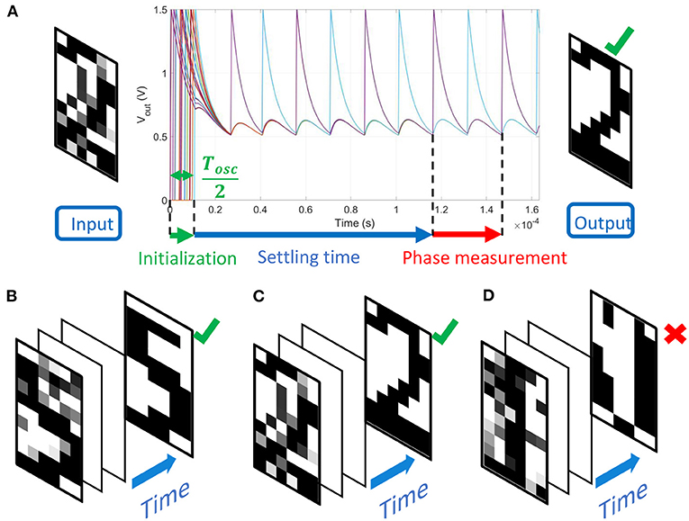
Figure 13. (A) Noisy input image “2” with 15 random altered pixels and voltage waveforms of 60 oscillators. ONN is initialized during Tosc/2 with the noisy input image. After few oscillation cycles, ONN settles, and phases are measured. ONN retrieves the correct output image that corresponds to the stored pattern “2.” (B) The input image “5” has been altered at 15 random pixel locations by a uniform distribution. ONN retrieves the corresponding stored pattern. (C) Similarly, 15 random pixels of the input image “2” are altered, and ONN retrieves the correct corresponding pattern. (D) In this example, 20 noisy input pixels are introduced to digit “1,” and ONN converges toward a spurious state.
3.1.3. ONN Recognition Accuracy
Here, we perform simulations to compute the pattern recognition accuracy of the 60-ONN. We randomly apply noise to training patterns to generate a test set. It consists of 20 different subsets Sk, kϵ{1, 2, .., 20} in which 60 different test patterns have k randomly located fuzzy input pixels. We vary the mapping function parameter β to assess its influence on ONN accuracy. We notice from Figure 14C that ONN achieves the best accuracy for an optimum value β = N/32 = 1.875. In this case, ONN recognizes more than 80% of test images with up to 20% of noise. As seen in Figure 12C, the slope parameter β sets the coupling resistance range, which in turn affects ONN accuracy. For instance, we observe that the set of coupling resistances obtained for β = 2 is similar to the case β = 2.5, but the accuracy is much lower in the latter case. In the next section, we quantify the coupling resistance accuracy that is required for synaptic design.
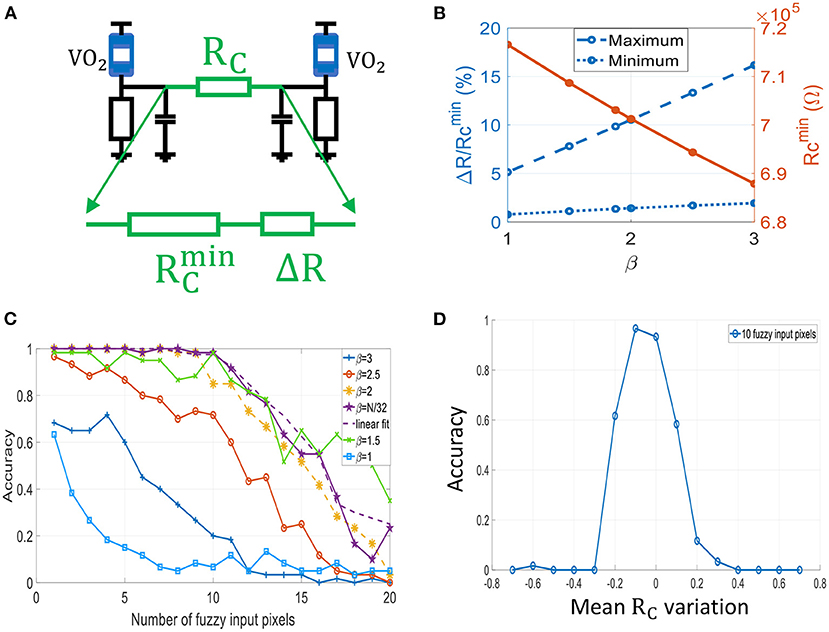
Figure 14. (A) Two oscillators coupled by RC, which can be decomposed in two series resistances: . (B) Evolution of ΔR, with respect to β. gives the best accuracy results. Note that . (C) ONN recognition accuracy for different values of β. The dashed line is obtained for a linear fit of the mapping μN, i.e., with coupling resistances that are linearly spaced. (D) Impact of RC's mean variation on recognition accuracy.
3.1.4. ONN Coupling Resistance Range
We study the impact of RC's relative variations and RC's mean value. is the minimum resistance common to all coupling resistances, and ΔR is the additional series resistance to distinguish between weights (Figure 14A). Using the Hebbian rule, weights are located near “0” coefficient as in Figure 12C and our mapping function can be fitted linearly (dashed lines). Therefore, every coupling resistances can be approximated by with nϵ{0, 1, 2, .., M}. Using this linear approximation, we can verify ONN accuracy is similar to the nominal case of mapping function with β = N/32, as shown in Figure 14C with the magenta dashed line.
As observed in previous sections, ONN accuracy is quite sensitive to the coupling resistances. We obtain for β = 3, and for β = 1 (Figure 14B). For these two cases as shown in Figure 14C, ONN shows poor accuracy. It is rather for β = N/32 = 1.875 with that ONN accuracy is above 90%.
To achieve the best ONN accuracy, a very good resistor matching is required, as we need a precision of between two consecutive weights. To study the influence of the RC's mean value only, we apply the same variation to all coupling resistances for β = N/32 and for 10 fuzzy input pixels (Figure 14D). We notice that the mean value of coupling resistances can vary from –10% up to +5% from its nominal value to achieve a similar accuracy.
4. Discussion
Oscillatory neural networks are triggering great interest for parallel processing applications, but a remaining challenge is how to compute with ONNs. To do so, we build analogies with ANN to determine the mapping between Hebbian learning coefficients (weights) to coupling resistors, knowing that they are essential elements for the network functionality. In this work, we proposed a mapping function that translates Hebbian signed weights to coupling resistances in a VO2-based ONN for systematic ONN analysis. Our simulations on 60-oscillators test case study highlighted a strong dependency between the ONN recognition accuracy and its coupling resistance range, set by mapping parameter β. Although we identified a suitable value β = N/32 to achieve good ONN accuracy, our mapping formulation provides coupling resistances that differ only with few percent. This would lead to significant hardware design constraints, as resistor mismatches smaller than 1.7% would be required to emulate two consecutive weights. In our mapping formalism, we used the phase transition function ζ, which provides the coupling resistance range holding the ONN memory. As we only derived ζ from oscillator dynamics, we believe the oscillator design could be optimized to expand the coupling resistance range and relax synaptic design constraints. For example, oscillator biasing current and supply voltage are the knobs that could be adjusted to maximize the synaptic range.
Here, we reported on a mapping function to compute coupling resistances from signed Hebbian coefficients in a VO2-based ONN. We first enhanced the ONN initialization control based on a simple architecture where every oscillator can be decoupled from the network via a switch. We were able to derive the phase transition function from the ONN dynamics, which is crucial for ONN memory. We then merged this analytical formulation with a sigmoid activation function from ANN formalism to build a mapping function. To demonstrate the ONN architecture's applicability with the proposed mapping function, we presented a test case of pattern recognition with 60 fully coupled oscillators. Finally, we showed that ONN recognition accuracy is very sensitive to relative variations between coupling resistances.
Data Availability Statement
The raw data supporting the conclusions of this article will be made available by the authors, without undue reservation.
Author Contributions
CD and AT-S developed the analytical formulation of ONN mapping and wrote the article. CD implemented the ONN circuit-solver framework on Matlab and performed simulations. Both authors contributed to the article and approved the submitted version.
Funding
This work is supported by the European Union's Horizon 2020 research and innovation program, EU H2020 NEURONN (www.neuronn.eu) project under Grant No. 871501.
Conflict of Interest
The authors declare that the research was conducted in the absence of any commercial or financial relationships that could be construed as a potential conflict of interest.
Publisher's Note
All claims expressed in this article are solely those of the authors and do not necessarily represent those of their affiliated organizations, or those of the publisher, the editors and the reviewers. Any product that may be evaluated in this article, or claim that may be made by its manufacturer, is not guaranteed or endorsed by the publisher.
Supplementary Material
The Supplementary Material for this article can be found online at: https://www.frontiersin.org/articles/10.3389/fnins.2021.694549/full#supplementary-material
References
Acebrón, J. A., Bonilla, L. L., Pérez Vicente, C. J., Ritort, F., and Spigler, R. (2005). The kuramoto model: a simple paradigm for synchronization phenomena. Rev. Mod. Phys. 77, 137–185. doi: 10.1103/RevModPhys.77.137
Corti, E., Cornejo Jimenez, J. A., Niang, K. M., Robertson, J., Moselund, K. E., Gotsmann, B., et al. (2021). Coupled vo2 oscillators circuit as analog first layer filter in convolutional neural networks. Front. Neurosci. 15:19. doi: 10.3389/fnins.2021.628254
Corti, E., Gotsmann, B., Moselund, K., Stolichnov, I., Ionescu, A., and Karg, S. (2018). “Resistive coupled vo2 oscillators for image recognition,” in 2018 IEEE International Conference on Rebooting Computing (ICRC) (McLean, VA: IEEE), 1–7.
Corti, E., Gotsmann, B., Moselund, K., Stolichnov, I., Ionescu, A., Zhong, G., et al. (2019). “Vo2 oscillators coupling for neuromorphic computation,” in 2019 Joint International EUROSOI Workshop and International Conference on Ultimate Integration on Silicon (EUROSOI-ULIS) (Grenoble: IEEE), 1–4.
Corti, E., Khanna, A., Niang, K., Robertson, J., Moselund, K. E., Gotsmann, B., et al. (2020). Time-delay encoded image recognition in a network of resistively coupled vo on si oscillators. IEEE Electron. Device Lett. 41, 629–632. doi: 10.1109/LED.2020.2972006
Endo, T., and Takeyama, K. (1992). Neural network using oscillators. Electron. Commun. Jpn. 75, 51–59. doi: 10.1002/ecjc.4430750505
Fell, J., and Axmacher, N. (2011). The role of phase synchronization in memory processes. Nat. Rev. Neurosci. 12, 105–118. doi: 10.1038/nrn2979
Gerstner, W., Kistler, W. M., Naud, R., and Paninski, L. (2014). Neuronal Dynamics: From Single Neurons to Networks and Models of Cognition, Chapter 17.2. New York, NY; Cambdrige University Press.
Hopfield, J. J. (1982). Neural networks and physical systems with emergent collective computational abilities. Proc. Natl. Acad. Sci. U.S.A. 79, 2554–2558. doi: 10.1073/pnas.79.8.2554
Hoppensteadt, F. C., and Izhikevich, E. M. (2000). Pattern recognition via synchronization in phase-locked loop neural networks. IEEE Trans. Neural Netw. 11, 734–738. doi: 10.1109/72.846744
Izhikevich, E., and Kuramoto, Y. (2006). Weakly coupled oscillators. Encyclopedia Math. Phys. 448–53. doi: 10.1016/B0-12-512666-2/00106-1
Jackson, T., Pagliarini, S., and Pileggi, L. (2018). “An oscillatory neural network with programmable resistive synapses in 28 nm CMOS,” in 2018 IEEE International Conference on Rebooting Computing (ICRC) (McLean, VA: IEEE), 1–7.
Maffezzoni, P., Bahr, B., Zhang, Z., and Daniel, L. (2015a). Oscillator array models for associative memory and pattern recognition. IEEE Trans. Circ. Syst. I Regul. Pap. 62, 1591–1598. doi: 10.1109/TCSI.2015.2418851
Maffezzoni, P., Bahr, B., Zhang, Z., and Daniel, L. (2016). Analysis and design of boolean associative memories made of resonant oscillator arrays. IEEE Trans. Circ. Syst. I Regul. Pap. 63, 1964–1973. doi: 10.1109/TCSI.2016.2596300
Maffezzoni, P., Daniel, L., Shukla, N., Datta, S., and Raychowdhury, A. (2015b). Modeling and simulation of vanadium dioxide relaxation oscillators. IEEE Trans. Circ. Syst. I Regul. Pap. 62, 2207–2215. doi: 10.1109/TCSI.2015.2452332
Nez, J., Avedillo, M. J., Jimnez, M., Quintana, J. M., Todri-Sanial, A., Corti, E., et al. (2021). Oscillatory neural networks using vo2 based phase encoded logic. Front. Neurosci. 15:442. doi: 10.3389/fnins.2021.655823
Parihar, A., Shukla, N., Datta, S., and Raychowdhury, A. (2015). Synchronization of pairwise-coupled, identical, relaxation oscillators based on metal-insulator phase transition devices: a model study. J. Appl. Phys. 117, 054902. doi: 10.1063/1.4906783
Parihar, A., Shukla, N., Jerry, M., Datta, S., and Raychowdhury, A. (2017). Vertex coloring of graphs via phase dynamics of coupled oscillatory networks. Sci. Rep. 7, 911. doi: 10.1038/s41598-017-00825-1
Raychowdhury, A., Parihar, A., Smith, G. H., Narayanan, V., Csaba, G., Jerry, M., et al. (2019). Computing with networks of oscillatory dynamical systems. Proc. IEEE 107, 73–89. doi: 10.1109/JPROC.2018.2878854
Schmitt, O. H. (1938). A thermionic trigger. J. Sci. Instrum. 15, 24–26. doi: 10.1088/0950-7671/15/1/305
Sharma, A. A., Bain, J. A., and Weldon, J. A. (2015). Phase coupling and control of oxide-based oscillators for neuromorphic computing. IEEE J. Exploratory Solid State Comput. Devices Circ. 1, 58–66. doi: 10.1109/JXCDC.2015.2448417
Shukla, N., Parihar, A., Cotter, M., Barth, M., Li, X., Chandramoorthy, N., et al. (2014). “Pairwise coupled hybrid vanadium dioxide-mosfet (hvfet) oscillators for non-boolean associative computing,” in 2014 IEEE International Electron Devices Meeting (San Francisco, CA: IEEE), 28.7.1–28.7.4.
Shukla, N., Tsai, W.-Y., Jerry, M., Barth, M., Narayanan, V., and Datta, S. (2016). “Ultra low power coupled oscillator arrays for computer vision applications,” in 2016 IEEE Symposium on VLSI Technology (Honolulu, HI: IEEE), 1–2.
Todri-Sanial, A., Carapezzi, S., Delacour, C., Abernot, M., Gil, T., Corti, E., et al (2021). How Frequency Injection Locking Can Train Oscillatory Neural Networks to Compute in Phase. Available online at: https://hal-lirmm.ccsd.cnrs.fr/lirmm-03164135 (accessed April 12, 2021).
Vassilieva, E., Pinto, G., de Barros, J., and Suppes, P. (2011). Learning pattern recognition through quasi-synchronization of phase oscillators. IEEE Trans. Neural Netw. 22, 84–95. doi: 10.1109/TNN.2010.2086476
Wang, H., Qi, M., and Wang, B. (2017). Ppv modeling of memristor-based oscillators and application to onn pattern recognition. IEEE Trans. Circ. Syst. II Express Briefs 64, 610–614. doi: 10.1109/TCSII.2016.2591961
Keywords: oscillatory neural network, VO2 device, coupled relaxation oscillators dynamics, Hopfield Neural Network, Hebbian learning rule, pattern recognition
Citation: Delacour C and Todri-Sanial A (2021) Mapping Hebbian Learning Rules to Coupling Resistances for Oscillatory Neural Networks. Front. Neurosci. 15:694549. doi: 10.3389/fnins.2021.694549
Received: 13 April 2021; Accepted: 14 October 2021;
Published: 08 November 2021.
Edited by:
Bipin Rajendran, King's College London, United KingdomReviewed by:
Zhijun Yang, Middlesex University, United KingdomNikhil Shukla, University of Virginia, United States
Copyright © 2021 Delacour and Todri-Sanial. This is an open-access article distributed under the terms of the Creative Commons Attribution License (CC BY). The use, distribution or reproduction in other forums is permitted, provided the original author(s) and the copyright owner(s) are credited and that the original publication in this journal is cited, in accordance with accepted academic practice. No use, distribution or reproduction is permitted which does not comply with these terms.
*Correspondence: Aida Todri-Sanial, YWlkYS50b2RyaUBsaXJtbS5mcg==