1 Introduction
Among the various platforms for quantum technologies, negatively charged nitrogen vacancy () centers in diamond are particularly attractive due to their operation at room temperature, solid-state integration, and compatibility with advanced nanofabrication techniques. These features make them uniquely suited for scalable quantum technologies, including quantum information processing, sensing, and nanoscale imaging. The center, a point defect consisting of a substitutional nitrogen atom adjacent to a vacant site in a diamond lattice, possesses electron spin states that can be optically initialized, manipulated and read out, even at room temperature (Jelezko et al., 2004). These characteristics enable a wide range of applications, including magnetometry (Balasubramanian et al., 2008; Katsumi et al., 2025), electrometry (Dolde et al., 2011), and thermometry (Neumann et al., 2013). They are also highly versatile, and schemes have been reported allowing for their use as sensitive magnetometers in zero bias field (Zheng et al., 2019) and without the use of microwave excitation (Wickenbrock et al., 2016; Bürgler et al., 2023). Recent demonstrations on the transfer of the spin polarization to proximal nuclear spins to create a spin register have also shown incredible promise for the future of these centers, with spin coherence times exceeding several seconds (Bradley et al., 2019; van de Stolpe et al., 2024). A key advantage of using centers lies in their nature as atomic-scale point defects in a solid-state host. Their minute size allows for nanometer scale precision in sensing, for example, allowing for the imaging of magnetic nanostructures and currents in microelectronic circuits.
Such applications, however, require deterministic placement of individual centers with minimal damage to the surrounding lattice. This has been accomplished using ultrafast laser writing, which allows centers to be fabricated with high spatial precision (Chen et al., 2017). The laser writing process consists of an initial seed pulse that produces vacancies in the lattice via multiphoton ionization, followed by a train of diffusion pulses, which cause vacancies to migrate until an center is formed. This method has been used to fabricate centers with an in-plane positioning accuracy of 33 nm and a depth distribution with a half-width-at-half-maximum (HWHM) of 197 nm (Chen et al., 2019).
However, laser writing results in centers oriented along any of the four possible axes, the [111], , , or axes. Random orientation is undesirable for many magnetometry applications, as each center is sensitive only to the component of the magnetic field parallel to its orientation axis. This results in an orientation-dependent Zeeman splitting such that only a single orientation can be resonantly addressed at once. Other orientations then contribute to the background, decreasing the contrast of measurements. Preferential orientation of centers along two axes has been demonstrated to increase the sensitivity of magnetometry with ensembles by a factor of 2 (Pham et al., 2012). CVD growth has been used to produce centers with preferential orientation along two axes in diamonds with (110)-(Edmonds et al., 2012) and (100)-oriented surfaces (Pham et al., 2012), and along a single axis for (111)-(Lesik et al., 2014; Michl et al., 2014; Fukui et al., 2014) and (113)-oriented surfaces (Lesik et al., 2015). To date, however, no method has been demonstrated for the production of well localized single centers with a specific orientation. The lack of post-fabrication orientation control has been an obstacle to scaling NV-based sensors, particularly in applications requiring uniform spin response such as vector magnetometry and high-contrast imaging of biological systems.
The center emits fluorescence (PL) via a linear combination of two orthogonal dipole moments in the plane normal to the center orientation axis. The dipoles are energetically degenerate, resulting in a nominally circular polarization pattern. However, they can contribute differently to the overall PL signal when analyzed through a polarizer in the laboratory reference frame due to their respective orientations relative to the diamond surface. Hence, polarization patterns can be used to characterize the orientation within the diamond lattice (Dolan et al., 2014). Due to the distinct dipole emission patterns in combination with diamond’s high refractive index, orientation also affects the luminescence intensity, and the orientation can also be determined by observing this change in intensity (Peng et al., 2024).
Here, we combine several of these ideas and introduce a femtosecond laser annealing technique that allows for reorientation of individual laser written centers. By selectively dissociating and reforming centers optically, all orientations are produced stochastically. By combining this with in situ orientation detection via fluorescence polarization analysis, this process then enables the selection of a desired crystallographic orientation, allowing for fully deterministic spatial and orientational control of single centers.
2 Methods
centers are fabricated using a home-built aberration-corrected ultrafast laser writing system with an in situ confocal microscope, as shown in Figure 1. The system uses 270 fs pulses at 515 nm generated by a Yb:KYW laser (Light Conversion Pharos PH2). Pulse energy is controlled using a waveplate (Thorlabs WPHSM05-514) and a Glan-laser polarizer (Thorlabs GL5). The beam is then expanded to fill a spatial light modulator (SLM) (dual-band Meadowlark HSP 1920-500-1200), which applies aberration corrections to compensate for the significant spherical aberration caused by diamond’s high refractive index (Simmonds et al., 2011). The corrected beam is then focused into the diamond using a 1.45 numerical aperture (NA) oil immersion objective lens (Olympus MPlanApo N 100x). The sample is mounted on high-precision translation stages (Zaber LDM060C for x-y, LDM040C for z; accuracy 1 μm, repeatability 80 nm) and widefield transmission imaging is performed using a CMOS camera (Thorlabs CS165MU/M).
The confocal fluorescence microscope shares the same objective lens as the laser writing system. Non-resonant excitation is provided by a 532 nm continuous-wave laser (Spectra Physics Millennia eV 15) which is scanned across the sample using galvanometric mirrors (Thorlabs QS7XY-AG) enabling spatially independent excitation relative to the fabrication focus. The emitted fluorescence is separated from both the excitation and fabrication wavelengths using a 550 nm longpass dichroic mirror (Thorlabs DMLP567), then coupled into an optical fiber for confocal optical sectioning. The collected fluorescence signal is directed either to a single-photon avalanche detector (SPAD) (Excelitas SPCM-AQRH-14), a spectrometer (Princeton Instruments SpectraPro HRS-750 with Blaze 400HR eXcelon camera), or a pair of SPADs arranged in a Hanbury Brown and Twiss (HBT) interferometer configuration for photon autocorrelation measurements. Both the laser writing system and confocal microscope are controlled via custom software written for a Field Programmable Gate Array (FPGA) (NI USB-7845R) with a user interface developed in LabVIEW and Python.
center fabrication was performed on diamond substrates from two sources: a crystal with a (111)-oriented surface purchased from Flawless Technical Diamonds (FTD), in which a array of centers was created, and a (100)-oriented diamond substrate provided by Great Lakes Crystal Technologies (GLCT), where a single reoriented center was produced. The (111)-oriented diamond was HPHT grown and contained 10 ppb substitutional nitrogen. The surface was polished to a surface roughness of 5 nm with a miscut angle of . The (100)-oriented diamond was CVD grown and contained 80 ppb substitutional nitrogen. The surface was polished to a surface roughness of 1 nm with a miscut angle of . The substitutional nitrogen grown into the substrates is the source of the nitrogen that was converted to centers during the laser writing process, and no additional nitrogen was implanted into the as-grown substrates. In both samples, centers were fabricated using an initial 270 fs seed pulse (1.47 nJ at 515 nm) to generate vacancies and interstitial carbon atoms via multiphoton ionization. This was followed by a 200 kHz train of 1.19 nJ diffusion pulses which mobilized vacancies until one combined with a substitutional nitrogen atom to form an center. Fluorescence intensity was monitored during this process, and the pulse train was terminated upon detection of an signal.
Polarization analysis of the fluorescence for orientation determination was achieved using a waveplate (Thorlabs WPHSM05-694) in front of a polarizing beam splitter (Thorlabs PBS252). By rotating the half-wave plate, the full polarization profile of the emitted light was measured. The different projections of the center’s emission dipoles onto the optical pupil enabled the identification of orientation based on the polarization pattern. All four orientations can be differentiated in this manner for diamond with a (111)-oriented surface, whereas only two sets of orientations are distinguishable for diamond with a (100)-oriented surface. If the measured orientation did not match the desired orientation, an additional annealing pulse train was applied, causing reorientation of the center. Polarization measurements were repeated to identify the new orientation. This process was repeated until the desired orientation was observed. The fabricated centers were then characterized using photoluminescence excitation spectroscopy and photon autocorrelation measurements. Occasionally, when reorientation did not readily occur after applying diffusion pulses for several minutes, a second seed pulse was applied to help the process.
3 Results and discussion
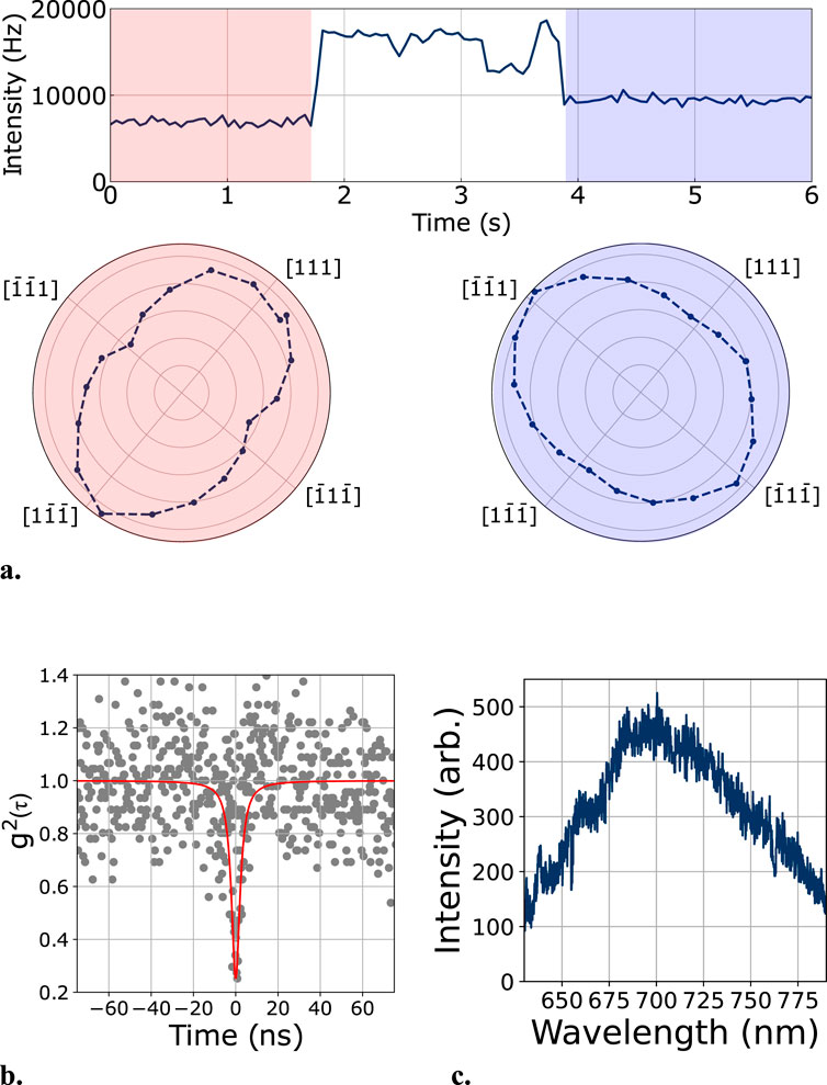
First, a single center was fabricated and reoriented in a (100)-oriented diamond substrate. The initial polarization signature of the center is shown in red in Figure 2a. Prior to reorientation, the half-waveplate in the fluorescence collection path was rotated to minimize the detected fluorescence signal. This provides polarization-dependent fluorescence contrast between the two distinguishable orientation classes observable in (100)-oriented diamond, allowing for quick reorientation detection. Figure 2a shows the time-resolved fluorescence signal during the reorientation process. The diffusion pulse train was activated at 1.8 s. A transient dip in fluorescence was observed just after the 3 s mark, followed by recovery to a higher fluorescence level. The diffusion pulse train was then terminated. The increased fluorescence observed after the reorientation process is consistent with the change in polarization and thus increased transmission through the polarization analyzer. The new orientation was confirmed by a full measurement of the polarization pattern as shown shaded in blue in Figure 2a. Single photon emission was verified by photon autocorrelation with an excitation laser power of 1.2 mW, yielding a background-corrected , as shown in Figure 2b. In (100)-oriented diamond, centers fall into two optically distinguishable orientation classes. This partial control over orientation enables the creation of arrays with only two orientations, potentially doubling the sensitivity in magnetometry applications (Pham et al., 2012). This degeneracy could be lifted by interrogation with radially polarized excitation (Dolan et al., 2014) or through optically detected magnetic resonance (ODMR).
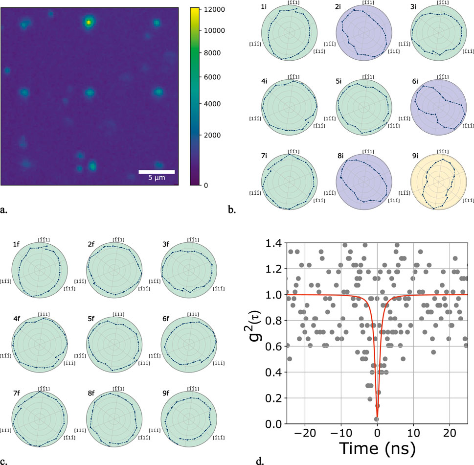
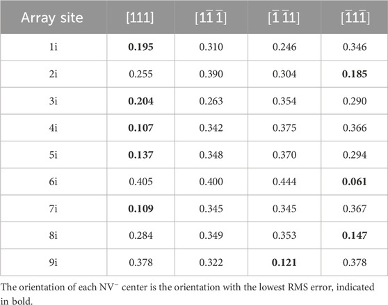
To fully exploit the ability to distinguish all four orientations, we extended our method to a (111)-oriented diamond substrate. Theoretical polarization patterns, shown in Figure 3, were calculated by rotating the center's two orthogonal emission dipoles from the coordinate system to the laboratory reference frame, projecting onto the [111] plane, then using the Jones calculus to simulate the fluorescence transmitted through the half-wave plate and polarizing beam splitter for each orientation, following the approach in (Hepp et al., 2014). Figure 3a illustrates idealized patterns with no background fluorescence, while Figure 3b shows patterns corresponding to a signal-to-noise ratio (SNR) of 3.5:1, matching the approximate average observed SNR to facilitate comparison with experimental results. An array of nine centers was fabricated with 10 µm pitch at a depth of 20 μm, as shown in Figure 4a. While shallow centers are typically optimal for sensing applications, the array was fabricated at 20 µm in order to minimize boiling and lensing effects in the immersion oil, which can disrupt fabrication. Potential methods to overcome this limitation include fabricating near the far surface of the diamond, writing using a solid-immersion lens (Yurgens et al., 2021), or polishing after fabrication to remove excess surface material. Qualitative polarization analysis (Figure 4b) revealed that five of the nine fabricated centers were initially oriented along the (111) crystallographic direction (i.e., parallel to the optical axis), while the remaining four centers were distributed among two of the three other possible orientations. The fourth orientation of the centers was absent, due to the limited number of centers in the fabricated array (but has been observed in other fabrication runs). Initial orientations were confirmed by demonstrating that the root mean square (RMS) error between the measured polarization patterns and the theoretical patterns for each orientation shown in Figure 3b is minimized for the identified orientation, as shown in Table 1.
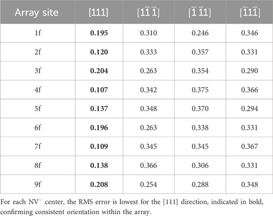
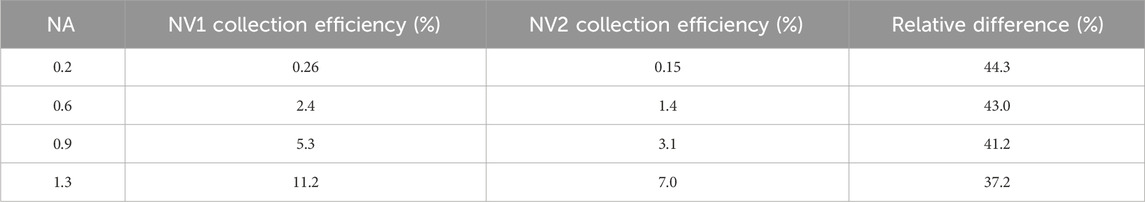
The reorientation process itself was identical to the (100) sample, with the exception that the polarization was not biased to minimize counts. Instead, a full polarization map was taken when fluctuations in the fluorescence level occurred. This was because the difference in fluorescence intensity using a single linear polarization analyzer between the four orientations does not provide a clear contrast in (111)-oriented diamond. Each center was reoriented to the (111) direction parallel to the optical axis (vertical), which was confirmed by polarization measurements shown in Figure 4c. Successful reorientation was further confirmed through RMS error calculations, shown in Table 2. Single photon emission from one of the sites (site 3f) was verified by photon autocorrelation with an excitation laser power of 0.45 mW, yielding a background-corrected as shown in Figure 4d. Note that the speed and simplicity of this process could in principle be improved further by splitting the fluorescence into multiple paths with separate polarization analyzers set to the individual orientation axes of (111)-oriented material. Comparison of the PL intensity in the individual arms could then provide quick feedback on the orientation without the need to measure a full polarization pattern.
Such an array aligned along the optical axis has two distinct advantages over an unaligned array. Firstly, it allows for each member of the array to be coherently addressed simultaneously under the same magnetic field. This would in principle lead to a factor of four increase in sensitivity when compared to a randomly oriented array. Secondly, centers aligned along the optical axis emit more light into a smaller NA of an objective lens and less light is lost during total internal reflection, ensuring both maximal light collection and reduction in non-symmetric aberrations accumulated at the diamond surface, improving sensitivity due to its enhanced photon collection. This improvement was estimated by calculating the light collection efficiencies from two centers into a fixed NA. NV1 has its high-symmetry axis (z-axis) aligned parallel to the optical axis (perpendicular to the sample surface). NV2 is rotated by 109. with respect to NV1. These two orientations reflect the two possible cases in a sample with (111) surface orientations. The main emission dipoles of the center are two orthogonal dipoles in the xy-plane, perpendicular to the high-symmetry axis. Assuming far-field emission , the emitted intensity was integrated over the solid angle for a given NA. Table 3 shows the collection efficiencies normalized by the total emitted power for NV1 and NV2 as well as their relative difference for a few common NAs. An array pitch of 10 µm was chosen due to evidence in the literature that the diffusion process can influence an area of diamond much larger than the focal spot (Cheng et al., 2024). Further investigations of the diffusion process are needed to minimize potential unwanted effects on neighboring centers, such as reorientation to an undesirable orientation, and reduce emitter spacing. Since the magnetic sensitivity of based devices scales with the number of centers as it is unlikely that an oriented array of laser written single centers written in this manner will a higher magnetic sensitivity than that of a densely grown ensemble of randomly oriented centers. However, the ability to reorient defects would prove useful in applications that employ photonic devices or that utilize single centers for high spatial resolution sensing (Balasubramanian et al., 2008; Maze et al., 2008; Casola et al., 2018).
Two potential, non-competing, mechanisms explain how reorientation occurs. Firstly, the initial center is dissociated during annealing, allowing a vacancy to migrate and reform an center in a new orientation (Pinto et al., 2012). This occurrence is proposed within the literature as the dominant mechanism by which NV centers migrate in diamond under thermal annealing, however it is yet to be determined if ultrafast laser diffusion is able to exceed the energy barrier required to dissociate an NV center in this process. Although this mechanism seems promising considering the reduction in fluorescence during diffusion demonstrated in Figure 2a, there may be other mechanisms that can cause an center to stop fluorescing without dissociation. Hybridization between the center’s e-manifold and the -bonds of a (100)-split carbon self-interstitial has been demonstrated and could reduce the fluorescence emission from the center (Kirkpatrick et al., 2024). Therefore, it is possible that the reorientation process is substantially different from the thermal mechanism, with the initial center continuing to exist initially but as a dark, modified defect-complex involving additional entities such as interstitials or vacancies, followed by a dissociation step of this intermediate defect, resulting in a reoriented center. Further evidence for such a process is the occasional need to reseed after prolonged, unsuccessful reorientation attempts. This is likely due to a lack of species in the vicinity of the NV center that catalyze the reorientation process, most likely additional vacancies. It is in principle possible to reorient any observed center. However, it is possible to inadvertently fabricate additional centers depending on the properties of the sample (e.g., substitutional nitrogen content) or to inadvertently produce graphite depending on the laser parameters used. These risks can be mitigated with careful sample selection and tuning of the laser parameters.
In conclusion, we have demonstrated a fully optical method for the deterministic orientation of single centers with high spatial resolution in diamond using femtosecond laser annealing. Using this method, we demonstrated the feasibility of fabricating oriented arrays of centers in diamonds in both (100)- and (111)-oriented diamond substrates. Being an all-optical process, ultrafast laser writing provides unique control of the defect formation process and defect properties. Such techniques provide invaluable flexibility in fabricating optimized spin-photonic systems. Future work in this field may extend these methods to other defects in diamond or other materials systems, potentially in combination with the preparation of suitable precursor materials. Moreover, further optimization is needed to make this process suitable for writing of shallow defects and direct writing into nanostructured diamond. Finally, a better understanding of the microscopic processes underpinning defect creation and dynamics in femtosecond laser fabrication via the development of theoretical models in combination with ultrafast spectroscopy is needed for further optimizations.
Data availability statement
The original contributions presented in the study are included in the article, further inquiries can be directed to the corresponding authors.
Author contributions
KK: Writing – original draft, Investigation, Visualization, Software. AK: Conceptualization, Writing – original draft, Investigation, Software, Visualization. YT: Resources, Project administration, Writing – review and editing, Conceptualization, Funding acquisition. JB: Resources, Conceptualization, Funding acquisition, Writing – review and editing, Supervision, Project administration. SN: Writing – review and editing, Project administration, Supervision, Funding acquisition, Resources, Conceptualization.
Funding
The author(s) declare that financial support was received for the research and/or publication of this article. This work was supported through a collaborative research agreement funded through Toyota Motor Engineering & Manufacturing, North America, Inc. JB was supported by the Cowen Family Endowment. KK acknowledges support from a Lawrence W. Hantel Endowed Fellowship at MSU.
Acknowledgments
We thank Great Lakes Crystal Technologies (GLCT) for providing a suitable diamond sample for this work and Paul Quayle for helpful comments.
Conflict of interest
Author YT was employed by Toyota Motor North America.
The remaining authors declare that the research was conducted in the absence of any commercial or financial relationships that could be construed as a potential conflict of interest.
Generative AI statement
The author(s) declare that no Generative AI was used in the creation of this manuscript.
Any alternative text (alt text) provided alongside figures in this article has been generated by Frontiers with the support of artificial intelligence and reasonable efforts have been made to ensure accuracy, including review by the authors wherever possible. If you identify any issues, please contact us.
Publisher’s note
All claims expressed in this article are solely those of the authors and do not necessarily represent those of their affiliated organizations, or those of the publisher, the editors and the reviewers. Any product that may be evaluated in this article, or claim that may be made by its manufacturer, is not guaranteed or endorsed by the publisher.
References
Balasubramanian, G., Chan, I. Y., Kolesov, R., Al-Hmoud, M., Tisler, J., Shin, C., et al. (2008). Nanoscale imaging magnetometry with diamond spins under ambient conditions. Nature 455, 648–651. doi:10.1038/nature07278
PubMed Abstract | CrossRef Full Text | Google Scholar
Bürgler, B., Sjolander, T. F., Brinza, O., Tallaire, A., Achard, J., and Maletinsky, P. (2023). All-optical nuclear quantum sensing using nitrogen-vacancy centers in diamond. npj Quantum Inf. 9, 56. doi:10.1038/s41534-023-00724-6
PubMed Abstract | CrossRef Full Text | Google Scholar
Bradley, C. E., Randall, J., Abobeih, M. H., Berrevoets, R. C., Degen, M. J., Bakker, M. A., et al. (2019). A ten-qubit solid-state spin register with quantum memory up to one minute. Phys. Rev. X 9, 031045. doi:10.1103/PhysRevX.9.031045
CrossRef Full Text | Google Scholar
Casola, F., van der Sar, T., and Yacoby, A. (2018). Probing condensed matter physics with magnetometry based on nitrogen-vacancy centres in diamond. Nat. Rev. Mater. 3, 17088. doi:10.1038/natrevmats.2017.88
CrossRef Full Text | Google Scholar
Chen, Y.-C., Salter, P. S., Knauer, S., Weng, L., Frangeskou, A. C., Stephen, C. J., et al. (2017). Laser writing of coherent colour centres in diamond. Nat. Photonics 11, 77–80. doi:10.1038/nphoton.2016.234
CrossRef Full Text | Google Scholar
Chen, Y.-C., Griffiths, B., Weng, L., Nicley, S. S., Ishmael, S. N., Lekhai, Y., et al. (2019). Laser writing of individual nitrogen-vacancy defects in diamond with near-unity yield. Optica 6, 662. doi:10.1364/OPTICA.6.000662
CrossRef Full Text | Google Scholar
Cheng, X., Thurn, A., Chen, G., Jones, G. S., Coke, M., Adshead, M., et al. (2024). Laser activation of single group-iv colour centres in diamond. Nat Commun. 16, 5124. doi:10.1038/s41467-025-60373-5
PubMed Abstract | CrossRef Full Text | Google Scholar
Dolan, P. R., Li, X., Storteboom, J., and Gu, M. (2014). Complete determination of the orientation of NV centers with radially polarized beams. Opt. Express 22, 4379–4387. doi:10.1364/OE.22.004379
PubMed Abstract | CrossRef Full Text | Google Scholar
Dolde, F., Fedder, H., Doherty, M. W., Nöbauer, T., Rempp, F., Balasubramanian, G., et al. (2011). Electric-field sensing using single diamond spins. Nat. Phys. 7, 459–463. doi:10.1038/nphys1969
CrossRef Full Text | Google Scholar
Edmonds, A. M., Dâhaenens-Johansson, U. F. S., Cruddace, R. J., Newton, M. E., Fu, K.-M. C., Santori, C., et al. (2012). Production of oriented nitrogen-vacancy color centers in synthetic diamond. Phys. Rev. B 86, 035201. doi:10.1103/PhysRevB.86.035201
CrossRef Full Text | Google Scholar
Fukui, T., Doi, Y., Miyazaki, T., Miyamoto, Y., Kato, H., Matsumoto, T., et al. (2014). Perfect selective alignment of nitrogen-vacancy centers in diamond. Appl. Phys. Express 7, 055201. doi:10.7567/APEX.7.055201
CrossRef Full Text | Google Scholar
Hepp, C., Müller, T., Waselowski, V., Becker, J. N., Pingault, B., Sternschulte, H., et al. (2014). Electronic structure of the silicon vacancy color center in diamond. Phys. Rev. Lett. 112, 036405. doi:10.1103/PhysRevLett.112.036405
PubMed Abstract | CrossRef Full Text | Google Scholar
Jelezko, F., Gaebel, T., Popa, I., Gruber, A., and Wrachtrup, J. (2004). Observation of coherent oscillations in a single electron spin. Phys. Rev. Lett. 92, 076401. doi:10.1103/PhysRevLett.92.076401
PubMed Abstract | CrossRef Full Text | Google Scholar
Katsumi, R., Takada, K., Kawai, K., Sato, D., and Yatsui, T. (2025). High-sensitivity nanoscale quantum sensors based on a diamond micro-resonator. Commun. Mater. 6, 49. doi:10.1038/s43246-025-00770-x
CrossRef Full Text | Google Scholar
Kirkpatrick, A. R., Chen, G., Witkowska, H., Brixey, J., Green, B. L., Booth, M. J., et al. (2024). Ab initio study of defect interactions between the negatively charged nitrogen vacancy centre and the carbon self-interstitial in diamond. Philosophical Trans. R. Soc. A Math. Phys. Eng. Sci. 382, 20230174. doi:10.1098/rsta.2023.0174
PubMed Abstract | CrossRef Full Text | Google Scholar
Lesik, M., Tetienne, J.-P., Tallaire, A., Achard, J., Mille, V., Gicquel, A., et al. (2014). Perfect preferential orientation of nitrogen-vacancy defects in a synthetic diamond sample. Appl. Phys. Lett. 104, 113107. doi:10.1063/1.4869103
CrossRef Full Text | Google Scholar
Lesik, M., Plays, T., Tallaire, A., Achard, J., Brinza, O., William, L., et al. (2015). Preferential orientation of NV defects in CVD diamond films grown on (113)-oriented substrates. Diam. Relat. Mater. 56, 47–53. doi:10.1016/j.diamond.2015.05.003
CrossRef Full Text | Google Scholar
Maze, J. R., Stanwix, P. L., Hodges, J. S., Hong, S., Taylor, J. M., Cappellaro, P., et al. (2008). Nanoscale magnetic sensing with an individual electronic spin in diamond. Nature 455, 644–647. doi:10.1038/nature07279
PubMed Abstract | CrossRef Full Text | Google Scholar
Michl, J., Teraji, T., Zaiser, S., Jakobi, I., Waldherr, G., Dolde, F., et al. (2014). Perfect alignment and preferential orientation of nitrogen-vacancy centers during chemical vapor deposition diamond growth on (111) surfaces. Appl. Phys. Lett. 104, 102407. doi:10.1063/1.4868128
CrossRef Full Text | Google Scholar
Neumann, P., Jakobi, I., Dolde, F., Burk, C., Reuter, R., Waldherr, G., et al. (2013). High-precision nanoscale temperature sensing using single defects in diamond. Nano Lett. 13, 2738–2742. doi:10.1021/nl401216y
PubMed Abstract | CrossRef Full Text | Google Scholar
Peng, D. Y. M., Worboys, J. G., Sun, Q., Li, S., Capelli, M., Onoda, S., et al. (2024). All-optical determination of one or two emitters using polarization-enhanced photon correlations of nitrogen-vacancy centers in diamond. Phys. Rev. A 109, 023723. doi:10.1103/PhysRevA.109.023723
CrossRef Full Text | Google Scholar
Pham, L. M., Bar-Gill, N., Le Sage, D., Belthangady, C., Stacey, A., Markham, M., et al. (2012). Enhanced metrology using preferential orientation of nitrogen-vacancy centers in diamond. Phys. Rev. B 86, 121202. doi:10.1103/PhysRevB.86.121202
CrossRef Full Text | Google Scholar
Pinto, H., Jones, R., Palmer, D. W., Goss, J. P., Briddon, P. R., and Öberg, S. (2012). On the diffusion of nv defects in diamond. Phys. status solidi (a) 209, 1765–1768. doi:10.1002/pssa.201200050
CrossRef Full Text | Google Scholar
Simmonds, R. D., Salter, P. S., Jesacher, A., and Booth, M. J. (2011). Three dimensional laser microfabrication in diamond using a dual adaptive optics system. Opt. Express 19, 24122–24128. doi:10.1364/OE.19.024122
PubMed Abstract | CrossRef Full Text | Google Scholar
van de Stolpe, G. L., Kwiatkowski, D. P., Bradley, C. E., Randall, J., Abobeih, M. H., Breitweiser, S. A., et al. (2024). Mapping a 50-spin-qubit network through correlated sensing. Nat. Commun. 15, 2006. doi:10.1038/s41467-024-46075-4
PubMed Abstract | CrossRef Full Text | Google Scholar
Wickenbrock, A., Zheng, H., Bougas, L., Leefer, N., Afach, S., Jarmola, A., et al. (2016). Microwave-free magnetometry with nitrogen-vacancy centers in diamond. Appl. Phys. Lett. 109, 053505. doi:10.1063/1.4960171
CrossRef Full Text | Google Scholar
Yurgens, V., Zuber, J. A., FlÃ¥gan, S., De LucaBrendan, M., Shields, B. J., Zardo, I., et al. (2021). Low-charge-noise nitrogen-vacancy centers in diamond created using laser writing with a solid-immersion lens. ACS Photonics 8, 1726–1734. doi:10.1021/acsphotonics.1c00274
CrossRef Full Text | Google Scholar
Zheng, H., Xu, J., Iwata, G. Z., Lenz, T., Michl, J., Yavkin, B., et al. (2019). Zero-field magnetometry based on nitrogen-vacancy ensembles in diamond. Phys. Rev. Appl. 11, 064068. doi:10.1103/PhysRevApplied.11.064068
CrossRef Full Text | Google Scholar
 Kai Klink1,2
 Andrew Raj Kirkpatrick1,2
 Yukihiro Tadokoro3
 Jonas Nils Becker1,4*†
 Shannon Singer Nicley2,4,5*†
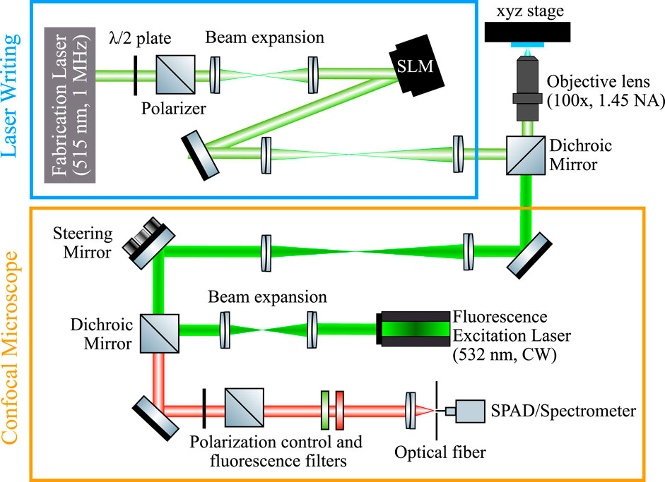
![Two sets of four polar plots, labeled (a) and (b). Each set shows circular graphs with varying blue line patterns, displaying different symmetrical shapes. The first shape in each set is circular, while the remaining shapes have two lobes. Both sets are marked with three different equivalent [111] crystallographic directions at three points around the circles, indicating the orientation of the graphs with the lobe maxima at these points. The lobes in (a) show greater contrast than those in (b).](https://www.frontiersin.org/files/Articles/1667545/frqst-04-1667545-HTML/image_m/frqst-04-1667545-g003.jpg)