 Xiyue Tian
 Zewei Luo
 Xing Wu
- Shanghai Key Laboratory of Multidimensional Information Processing, School of Communication and Electronic Engineering, East China Normal University, Shanghai, China
With the advent of smart flexible electronic devices, new research directions have emerged. Among them, the resistive switching (RS) sensor has attracted much attention. The RS sensor converts the change of voltage signals into the change of resistance values. In this work, a planar flexible RS structure based on one-step printable silver electrodes was designed and fabricated to simplify device fabrication. The study is a starting point that paves the way for the development of all-in-one printable and flexible sensors in the future.
Introduction
Recent years have seen the emergence of flexible electronic devices and applications such as the Internet of Things (Ko et al., 2008; Kim et al., 2018; Luo et al., 2019; Wu et al., 2019; Xu et al., 2019; Zhang et al., 2019). The flexible resistive switching (RS) device has a sandwich structure in which the top electrode, the active layer, and the bottom electrode are sequentially stacked. The fabrication process of the flexible RS device is usually bottom-up (Han and Lee, 2016). First, a bottom electrode is grown on a flexible substrate, after which a resistive layer material is deposited on the bottom electrode, and finally, a top electrode is deposited on the resistive layer. The electrodes of the RS device use metal materials such as copper (Zou et al., 2013), silver (Lee et al., 2019), and platinum (Tan et al., 2014), etc. and conductive oxide materials such as ITO (Midya et al., 2015) and FTO (Pham et al., 2018), etc. The fabrication processes of growing the electrode are usually performed by evaporation (Sun et al., 2016) or chemical vapor deposition (Giulia et al., 2019), which can be time-consuming, have a high thermal budget and consume a large amount of energy. The three-layer material of the sandwich structure is also prone to fracture during bending due to stress mismatch. Due to the fact that these sandwich-structure RS devices show high power consumption, complex fabrication processes, and limited applications, it is important to develop low-cost and simple-fabricated planar RS devices.
With the development of architecture, the planar RS devices with horizontal conductive paths have gradually exhibited advantages, such as the anti-crosstalk current between adjacent cells and the low-cost manufacturing process (Zhang et al., 2018). With horizontal grown conductive filament, a TiN/HfOx/Ti/HfOx/TiN-based RS device is fabricated by the nanodamascene process and shows the ability to avoid sneak current flow through neighboring cells (Labalette et al., 2017). For vertical devices, the leakage current path exists in an RS device with a low resistance state (LRS) (Linn et al., 2010). The series connection of two planar complementary-RS (CRS) devices A and B provide the solution. The CRS state shows “0” with a high resistance state (HRS)-A and LRS-B and the CRS state shows “1” with HRS-B and LRS-A. Regardless of the state, the total resistance of the planar CRS device is HRS, enabling it to avoid sneak current flowing. Flexible electronic printing technology is used to fabricate planar RS devices. Printable electronics are a promising manufacturing technology in the potential fabrication of flexible electronic devices such as flexible sensors (Lin et al., 2019), superconductors (Li et al., 2020), and thin-film transistors (Scholz et al., 2020), as result of the potential large-scale integration, low cost, and the fact that the technology is easy to operate (Li et al., 2019; Zhuldybina et al., 2020). An all-printed, flexible, and rewritable RS device was reported by Rehman et al. (2017). The silver electrodes were patterned by the reverse offset printing system and sprayed with graphene quantum dots (GQD) combined with white graphene (hBN). Fabricated by printed hBN flakes, embedded with GQD as the functional layer, the planar RS device shows stress match, large electrical endurance (1,000 cycles), and enhanced lifetime (105 s).
This study reports a printable and flexible silver-based planar RS sensory device array in which the metal electrodes are in firm contact with the substrate, without stress mismatch, and the process does not require high-temperature heating. Figure 1 is the schematic of the planar RS device in electrical performance, optical photograph, array integration, and outlook in artificial intelligence. This planar RS device demonstrates a more economical fabrication process and resistive switching performance.
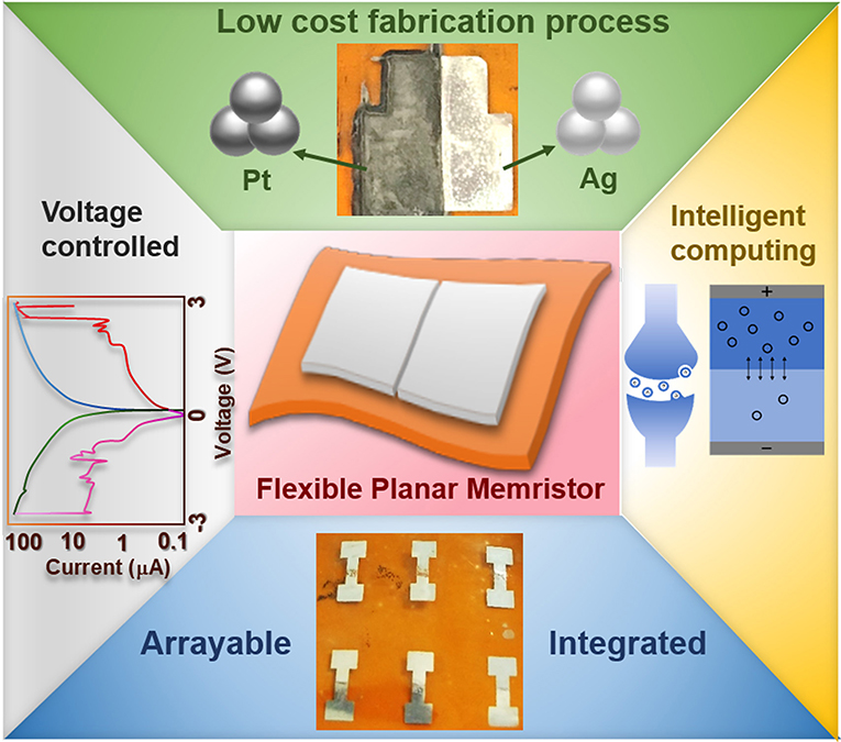
Figure 1. Schematic of the flexible planar RS device in electrical performance, optical photograph, array integration, and the outlook in artificial intelligence.
Materials and Methods
Materials
The materials used to fabricate the RS device include polyimide (PI) film (thickness: 100 μm), potassium hydroxide (AR, 85%), silver nitrate (AR, 98%), ammonia (AR, 25–28%), sodium borohydride (AR, 98%), hydrogen peroxide (AR, 30%), and chloroplatinic acid (AR, Pt > 37.5%). The etch tool and the mask are made of blade (width: 0.2 mm) and tape, respectively. The PI film was purchased from Qian Feng Insulating Material Company. Potassium hydroxide, silver nitrate, sodium borohydride, chloroplatinic acid, and hydrogen peroxide were purchased from the Aladdin Industrial Corporation. Ammonia was purchased from the Enox Company. The blade and the tape were obtained from the Flying Eagle Brand and Deli, respectively.
RS Device Fabrication
Figure 2 shows the schematic of the planar RS device fabrication procedure (Yu et al., 2015). First, the polyimide (PI) was successively immersed in 4 mol/L potassium hydroxide aqueous solution and 0.02 mol/L silver ammonia reagent. The surface of the PI film with dangling silver ions is shown in Figure 2A. Then, we used printed ink as a mask and dripped 0.02 mol/L hydrogen peroxide solution on the PI film to reduce the patterned silver as illustrated in Figure 2B. The low-hardness silver was easily removed by mechanical etching. As is shown in Figure 2C, the silver surface was etched with a sharp blade. The fine channels on the surface of the silver were obtained by mechanical etching, as shown in Figure 2D. As demonstrated in Figure 2E, we used the tape as the mask to protect a portion of the silver on the polyimide from reacting with the platinum ion. The chloroplatinic acid solution (mass fraction: 1%) was then dropped to the unprotected silver to complete the replacement reaction. The sample was next placed on a heating platform at 60°C for drying, as shown in Figure 2F. The platinum was reduced by soaking it in a 10 mmol/L sodium borohydride solution for 30 min. The bright part was silver, and the dark gray part was the reduced metal platinum. As demonstrated in Figure 2G, as in the mechanical etching of silver, the sharp blade was used for etching at the interface between the platinum and silver. The obtained fine channel is shown in Figure 2H. As shown in the enlarged section below, silver and platinum were on either side of the channel.
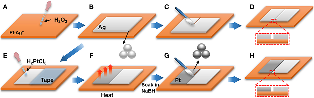
Figure 2. Schematic of the fabrication process of the planar RS device. (A) The fabrication process of growing silver by reducing the Ag+ in the modified polyimide with hydrogen peroxide. (B) Schematic of silver grown in PI substrate. (C) Channels made by mechanical blade-cutting. (D) Schematic of Ag-Ag planar RS device based on mechanical cutting manufacturing. (E,F) The fabrication process of growing platinum on silver. (G) Channels made by mechanical blade-cutting. (H) Schematic of Pt-Ag planar RS, based on mechanical cutting manufacturing.
Measurement Setup
The X-ray energy spectrum (EDS) and scanning electron microscope (SEM) were completed using the FEI XL30 FEG. Electrical experiments were completed by the electrochemical workstation (CHI660E). When testing the silver-silver (Ag-Ag) RS device, the two electrodes separated by the channel were connected to the working electrode and the reference electrode of the electrochemical workstation randomly. The Ag electrode was connected to the working electrode and the Pt electrode was connected to the reference electrode with silver-platinum (Ag-Pt) RS device measurement. The electrochemical workstation was used to apply voltage to the RS device and record the real-time current passing through the RS device.
Results
Characterization
The composition and microstructure of the silver surface after mechanical etching, the X-ray energy spectrum (EDS), and scanning electron microscope (SEM) images are shown in Figure 3. Figure 3A shows the microstructure of the channel in HRS at a 50 μm scale. The area with deep contrast shows high conductivity (Moncrieff et al., 1978; Wang et al., 2012), which is related to the conductivity of silver. At the mechanically etched channels, the distribution of silver was reduced. The blade removes part of the silver and exposes the PI substrate which contains carbon and oxygen. The areas with shallow contrast show poor conductivity, which is related to the exposed PI. Figure 3B shows the SEM image of the planar RS device in LRS at a 50 μm scale. The silver and polyimide were interlaced. The inset of Figure 3B shows the silver element distribution EDS image of the Ag-Ag planar RS device.
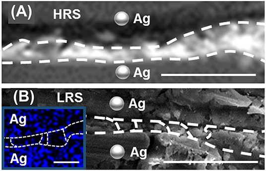
Figure 3. Characterization of planar silver electrodes-based RS device. (A) The SEM image of the high resistance state (HRS). (B) The SEM image of the low resistance state (LRS). The inset shows the EDS image of the LRS about Ag with a scale of 125 μm.
Performance
To test the set voltage, the reset voltage, the ON/OFF ratio, and the effect of bending of the Ag-Ag planar RS device, a series of electrical experiments were carried out. As illustrated in Figure 4A, a typical nonvolatile rewritable resistive switching behavior was found from the resistive switching performance plot of the planar RS device with the ON/OFF ratio of ~50. The applied voltage sweeps follow the arrows (0 V to +3 V to 0 V to −3 V to 0 V). The planar RS device is in the HRS from 0 V to the operating voltage of ~2.5 V and the conductivity decreases when the voltage increased to −2.9 V, which shows bipolar conversion characteristics. The low operating voltage shows low operating power consumption compared with the flexible RS devices (Kim et al., 2019). Figure 4B shows the resistive switching performance of another planar RS device with the same structure for four cycles with an applied voltage of −0.8–3 V. The planar RS device sets to the low resistance state between 0.75 and 1.75 V. At ~0 V, the planar RS device resets to a high resistance state, which shows unipolar conversion characteristics. Commonly, on-set potential is different in the different cycle tests of one RS device (He et al., 2009). There are two possible reasons for the different on-set potential of the silver electrodes-based RS device. First, the interface of the channel is irregular as demonstrated in Figure 3A, there may be multiple conduction paths, and the conductive paths in different cycles are not unique. After resetting it by applying voltage, the silver ions cannot completely return to the same position as no voltage is applied. For the conductive path, the initial position of the movable silver ion is different (Liu et al., 2012). Figures 4C,D show the results of one device placed flat and bent. The planar RS device has a flat placed state and the curved state shows similar switching performances.
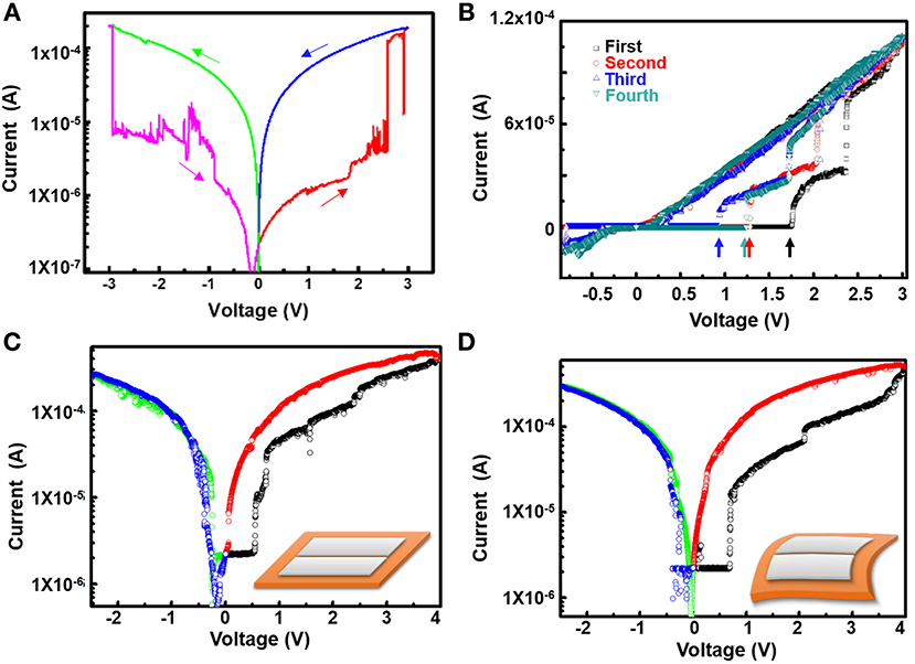
Figure 4. The electrical test of the Ag-Ag planar RS device. (A) Current-voltage characteristics of the planar RS device. (B) Repeatability and reset test of the planar RS device. (C) The current-voltage test of the explanted planar RS device. (D) The current-voltage test of the curving planar RS device.
Discussion
For RS devices, metal ion migration(Tian et al., 2014) and defect vacancy migration (Pham et al., 2018) are common reasons for resistance switching. With inactive electrodes, such as ITO and platinum, etc., the defect vacancies in the active RS layer trap carriers under the control of voltage, thereby forming conductive paths and reducing the resistance of the RS layer (Tan et al., 2014). With the active metal electrodes, such as silver, and copper, etc., the metal atoms are excited to ion state, and the ions migrate and connect, controlled by electric potential, thereby forming a conductive filament (Liu et al., 2012). To determine whether the conducting filaments are formed from the silver atoms or the defect vacancies, a series of comparative experiments and discussions are given in Figure 5. Platinum is commonly used as an inert electrode for RS devices. Figure 5A shows the resistive switching performance plot of the Pt-Ag planar RS device. The applied voltage sweeps, following as 0 V to +3 V to 0 V to −3 V to 0 V. The Pt-Ag planar has high resistance of ~1.18 × 10⁷ Ω, low resistance of ~9.5 × 10³ Ω, and the ON/OFF ratio of ~1.2 × 10³, which shows better performance compared to the flexible graphene-based RS device with an ON/OFF ratio of 3 (Midya et al., 2015). Figure 5B shows the resistive switching performance of the platinum-platinum (Pt-Pt) planar structure. The current show nanoamps order without hysteresis during the entire voltage switching test. Typical nonvolatile rewritable resistive switching behavior cannot perform in the Pt-Pt planar structure.
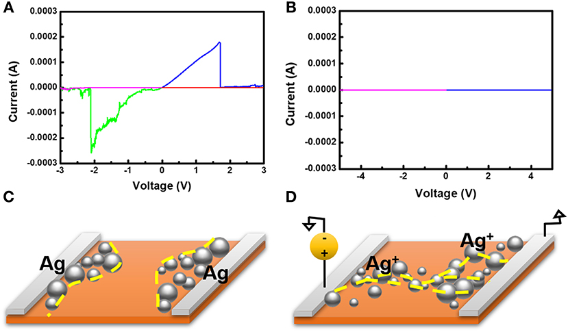
Figure 5. Mechanism analysis of the planar RS device. (A) The electrical reliability test of the Pt-Ag planar RS device. (B) The electrical reliability test of the Pt-Pt planar structure. (C) Schematic of Ag-Ag planar RS device without voltage. (D) The schematic of Ag+ in Ag-Ag planar RS device with voltage.
In an active electrode, silver metal ions can migrate in the resistive layer so that the resistance state of the RS device changes (Hirose and Hirose, 1976), and platinum is an inert electrode that only acts as an electrical conductor, which makes the Ag-Ag, Ag-Pt, and Pt-Pt planar RS device structures show different resistive switching performance. With the active electrode, the filament growth is completed by the migration of metal ions (Yang and Lu, 2016). With two inert electrodes, neither metal ion migration nor oxygen vacancy migration occurred, which can cause RS failure in Pt-Pt devices (Lanza et al., 2019). The schematic of the mechanism of resistance change in the Ag-Ag planar RS device is shown in Figures 5C,D (Peng et al., 2013; Fang et al., 2014). The insulating PI separates the conductive silver in the initial state with no voltage. The Ag-Ag planar RS device is in the high resistance state. As the voltage increases, silver ions migrate in the insulating polyimide and crosslink with the silver in other regions to form current paths. The Ag-Ag planar RS device is in the low resistance state.
Conclusion
Thus, study designed a planar silver-based RS device with an economical fabrication process and good performance, which provides a new perspective on the integration of smart printable flexible devices. The planar silver-based RS device shows a low operating voltage of 2.5 V and a high ON/OFF ratio of 1.2 × 10³. The RS performance is caused by the migration of silver ions. This study paves the way for future all-in-one flexible computing and memory integration systems.
Data Availability Statement
The original contributions presented in the study are included in the article/supplementary materials, further inquiries can be directed to the corresponding author/s.
Author Contributions
XW conceived and designed the review. XT, ZL, TF, JZ, and JC wrote the manuscript. All authors contributed to the article and approved the submitted version.
Funding
This work was supported by grants from the Projects of Science and Technology Commission of Shanghai Municipality (Nos. 19ZR1473800 and 14DZ2260800), the Young Elite Scientists Sponsorship Program of CAST (YESS), and Fundamental Research Funds for the Central Universities.
Conflict of Interest
The authors declare that the research was conducted in the absence of any commercial or financial relationships that could be construed as a potential conflict of interest.
References
Fang, Y., Zhigang, Z., Jer-Chyi, W., Liyang, P., Jun, X., and Chao-Sung, L. (2014). Total ionizing dose (TID) effects of γ ray radiation on switching behaviors of Ag/AlOx/Pt RRAM device. Nanoscale Res. Lett. 9:452. doi: 10.1186/1556-276X-9-452
Giulia, C., Busby, Y., Franquet, A., Spampinato, V., Houssiau, L., Bonfiglio, A., et al. (2019). A flexible organic memory device with a clearly disclosed resistive switching mechanism. Org. Electron. 64, 209–215. doi: 10.1016/j.orgel.2018.10.018
Han, U. B., and Lee, J. S. (2016). Integration scheme of nanoscale resistive switching memory using bottom-up processes at room temperature for high-density memory applications. Sci. Rep. 6:28966. doi: 10.1038/srep28966
He, C. L., Zhuge, F., Zhou, X. F., Li, M., Zhou, G. C., Liu, Y. W., et al. (2009). Nonvolatile resistive switching in graphene oxide thin films. Appl. Phys. Lett. 95:232101. doi: 10.1063/1.3271177
Hirose, Y., and Hirose, H. (1976). Polarity-dependent memory switching and behavior of Ag dendrite in Ag-photodoped amorphous As2S3films. J. Appl. Phys. 47, 2767–2772. doi: 10.1063/1.322942
Kim, T., Kim, D.-K., Kim, J., and Pak, J. J. (2019). Resistive switching behaviour of multi-stacked PVA/graphene oxide + PVA composite/PVA insulating layer-based RRAM devices. Semicond. Sci. Technol. 34:065006. doi: 10.1088/1361-6641/ab1403
Kim, Y., Chortos, A., Xu, W., Liu, Y., Oh, J. Y., Son, D., et al. (2018). A bioinspired flexible organic artificial afferent nerve. Science 360, 998–1003. doi: 10.1126/science.aao0098
Ko, H. C., Stoykovich, M. P., Song, J., Malyarchuk, V., Choi, W. M., Yu, C. J., et al. (2008). A hemispherical electronic eye camera based on compressible silicon optoelectronics. Nature 454, 748–753. doi: 10.1038/nature07113
Labalette, M., Jeannot, S., Blonkowski, S., Beilliard, Y., Ecoffey, S., Souifi, A., et al. (2017). Fabrication of planar back end of line compatible HfOx complementary resistive switches. IEEE Transact. Nanotechnol. 16, 745–751. doi: 10.1109/TNANO.2017.2698205
Lanza, M., Wong, H. S. P., Pop, E., Ielmini, D., Strukov, D., Regan, B. C., et al. (2019). Recommended methods to study resistive switching devices. Adv. Electron. Mater. 5:1800143. doi: 10.1002/aelm.201800143
Lee, B. R., Park, J. H., Lee, T. H., and Kim, T. G. (2019). Highly flexible and transparent memristive devices using cross-stacked oxide/metal/oxide electrode layers. ACS Appl. Mater Interfaces 11, 5215–5222. doi: 10.1021/acsami.8b17700
Li, J., Song, P., Zhao, J., Vaklinova, K., Zhao, X., Li, Z., et al. (2020). Printable two-dimensional superconducting monolayers. Nat. Mater. doi: 10.1038/s41563-020-00831-1. [Epub ahead of print].
Li, Q., Zhang, J., Li, Q., Li, G., Tian, X., Luo, Z., et al. (2019). Review of printed electrodes for flexible devices. Front. Mater. 5:77. doi: 10.3389/fmats.2018.00077
Lin, Y., Chen, J., Tavakoli, M. M., Gao, Y., Zhu, Y., Zhang, D., et al. (2019). Printable fabrication of a fully integrated and self-powered sensor system on plastic substrates. Adv. Mater. 31:e1804285. doi: 10.1002/adma.201804285
Linn, E., Rosezin, R., Kugeler, C., and Waser, R. (2010). Complementary resistive switches for passive nanocrossbar memories. Nat. Mater. 9, 403–406. doi: 10.1038/nmat2748
Liu, Q., Sun, J., Lv, H., Long, S., Yin, K., Wan, N., et al. (2012). Real-time observation on dynamic growth/dissolution of conductive filaments in oxide-electrolyte-based ReRAM. Adv. Mater. 24, 1844–1849. doi: 10.1002/adma.201104104
Luo, Z., Hu, X., Tian, X., Luo, C., Xu, H., Li, Q., et al. (2019). Structure-property relationships in graphene-based strain and pressure sensors for potential artificial intelligence applications. Sensors 19:1250. doi: 10.3390/s19051250
Midya, A., Gogurla, N., and Ray, S. K. (2015). Flexible and transparent resistive switching devices using Au nanoparticles decorated reduced graphene oxide in polyvinyl alcohol matrix. Curr. Appl. Phys. 15, 706–710. doi: 10.1016/j.cap.2015.03.008
Moncrieff, D. A., Robinson, V. N. E., and Harris, L. B. (1978). Charge neutralisation of insulating surfaces in the SEM by gas ionisation. J. Phys. D Appl. Phys. 11, 2315–2325. doi: 10.1088/0022-3727/11/17/002
Peng, H. Y., Pu, L., Wu, J. C., Cha, D., Hong, J. H., Lin, W. N., et al. (2013). Effects of electrode material and configuration on the characteristics of planar resistive switching devices. APL Mater. 1:052106. doi: 10.1063/1.4827597
Pham, N. K., Vu, N. H., Van Pham, V., Ta, H. K. T., Cao, T. M., Thoai, N., et al. (2018). Comprehensive resistive switching behavior of hybrid polyvinyl alcohol and TiO2 nanotube nanocomposites identified by combining experimental and density functional theory studies. J. Mater. Chem. C 6, 1971–1979. doi: 10.1039/C7TC05140A
Rehman, M. M., Siddiqui, G. U., Kim, S., and Choi, K. H. (2017). Resistive switching effect in the planar structure of all-printed, flexible and rewritable memory device based on advanced 2D nanocomposite of graphene quantum dots and white graphene flakes. J. Phys. D Appl. Phys. 50:335104. doi: 10.1088/1361-6463/aa798a
Scholz, A., Zimmermann, L., Gengenbach, U., Koker, L., Chen, Z., Hahn, H., et al. (2020). Hybrid low-voltage physical unclonable function based on inkjet-printed metal-oxide transistors. Nat. Commun. 11:5543. doi: 10.1038/s41467-020-19324-5
Sun, Y., Lu, J., Ai, C., and Wen, D. (2016). Nonvolatile memory devices based on poly(vinyl alcohol) + graphene oxide hybrid composites. Phys. Chem. Chem. Phys. 18, 11341–11347. doi: 10.1039/C6CP00007J
Tan, T., Guo, T., Chen, X., Li, X., and Liu, Z. (2014). Impacts of Au-doping on the performance of Cu/HfO2/Pt RRAM devices. Appl. Surf. Sci. 317, 982–985. doi: 10.1016/j.apsusc.2014.09.027
Tian, H., Chen, H. Y., Ren, T. L., Li, C., Xue, Q. T., Mohammad, M. A., et al. (2014). Cost-effective, transfer-free, flexible resistive random access memory using laser-scribed reduced graphene oxide patterning technology. Nano Lett. 14, 3214–3219. doi: 10.1021/nl5005916
Wang, L.-H., Yang, W., Sun, Q.-Q., Zhou, P., Lu, H.-L., Ding, S.-J., et al. (2012). The mechanism of the asymmetric SET and RESET speed of graphene oxide based flexible resistive switching memories. Appl. Phys. Lett. 100:063509. doi: 10.1063/1.3681366
Wu, F., Li, Q., Wang, P., Xia, H., Wang, Z., Wang, Y., et al. (2019). High efficiency and fast van der Waals hetero-photodiodes with a unilateral depletion region. Nat. Commun. 10:4663. doi: 10.1038/s41467-019-12707-3
Xu, S., Zou, X., Ma, B., Chen, J., Yu, L., and Zou, W. (2019). Deep-learning-powered photonic analog-to-digital conversion. Light Sci. Appl. 8:66. doi: 10.1038/s41377-019-0176-4
Yang, Y., and Lu, W. D. (2016). Progress in the characterizations and understanding of conducting filaments in resistive switching devices. IEEE Transact. Nanotechnol. 15, 465–472. doi: 10.1109/TNANO.2016.2544782
Yu, Y., Zhang, J., Wu, X., and Zhu, Z. (2015). Facile ion-exchange synthesis of silver films as flexible current collectors for micro-supercapacitors. J. Mater. Chem. A 3, 21009–21015. doi: 10.1039/C5TA04913J
Zhang, D., Li, T. R., Zhou, J. W., Jiang, Y. C., Ren, B., Huang, J., et al. (2018). Asymmetric resistive switching behaviour in a Au/a-C:Co/Au planar structure. Microelectron. Reliabil. 87, 52–56. doi: 10.1016/j.microrel.2018.05.021
Zhang, J., Yu, Y., Wang, P., Luo, C., Wu, X., Sun, Z., et al. (2019). Characterization of atomic defects on the photoluminescence in two-dimensional materials using transmission electron microscope. InfoMat 1, 85–97. doi: 10.1002/inf2.12002
Zhuldybina, M., Ropagnol, X., Bois, C., Zednik, R. J., and Blanchard, F. (2020). Printing accuracy tracking with 2D optical microscopy and super-resolution metamaterial-assisted 1D terahertz spectroscopy. npj Flex. Electron. 4:21. doi: 10.1038/s41528-020-00083-8
Keywords: computing and sensory integration systems, neural network, flexible devices, printable devices, resistive switching sensor array
Citation: Tian X, Luo Z, Fan T, Zhang J, Chu J and Wu X (2020) Printable and Flexible Planar Silver Electrodes-Based Resistive Switching Sensory Array. Front. Sens. 1:600185. doi: 10.3389/fsens.2020.600185
Received: 29 August 2020; Accepted: 30 November 2020;
Published: 18 December 2020.
Edited by:
Yuliya Semenova, Technological University Dublin, IrelandReviewed by:
Zegao Wang, Sichuan University, ChinaTessy Theres Baby, Karlsruhe Institute of Technology (KIT), Germany
Copyright © 2020 Tian, Luo, Fan, Zhang, Chu and Wu. This is an open-access article distributed under the terms of the Creative Commons Attribution License (CC BY). The use, distribution or reproduction in other forums is permitted, provided the original author(s) and the copyright owner(s) are credited and that the original publication in this journal is cited, in accordance with accepted academic practice. No use, distribution or reproduction is permitted which does not comply with these terms.
*Correspondence: Xing Wu, eHd1QGNlZS5lY251LmVkdS5jbg==