- 1Xinjiang Astronomical Observatory, Chinese Academy of Sciences, Urumqi, China
- 2University of Chinese Academy of Sciences, Beijing, China
- 3Xinjiang Key Laboratory of Microwave Technology Urumqi, Urumqi, China
This paper proposes a heterogeneous real-time baseband astronomical backend solution centered on RFSoC and combined GPU. The solution implemented the integration of the high-performance, completely configurable RF signal link to digitize, process, and transmit increasingly massive radio astronomy signals and provided a highly flexible and scalable scheme for the QTT backend. The RFSoC-based integration RF pre-processing front-end directly digitizes dual-polarization signals at the sampling rate of 2048 MHz and converts them to dual-16-channel data streams for parallel mixing and polyphase decimation filtering. The generated baseband data with 256 MHz center frequency and 100 MHz bandwidth is packaged and output to the GPU server through the 100GbE Interface. Complete processes of direct RF sampling, pre-processing, and high-speed transmission are implemented at the receiver. The GPU server executes real-time post-processing at the remote end. The dynamic configuration of two observation modes can be achieved with frequency resolutions of 3.051 and 0.763 kHz. The H2CO absorption line observations with the Nanshan 26-m radio telescope verified the system’s performance and the design’s rationality. This paper explores and confirms the RFSoC’s applicability on the backend. The flexible and efficient QTT backend scheme was planned based on the proposed real-time baseband pattern by expanding multi-RFSoC and GPU computing nodes.
1 Introduction
Construction of the Xinjiang 110-m Qitai radio telescope (QTT) began in September 2022 and will be completed within 6 years. QTT will equip ten ultra-wideband (UWB) receivers for 0.27GHz–115 GHz frequency coverage (MA et al., 2019) to observe and research various scientific targets such as spectral lines, pulsars, VLBI, astrometry and space positioning, galaxies and black holes, and dark matter (Wang et al., 2023). It poses higher requirements for developing the QTT backend for astronomical digital signal processing (DSP). It should not only address the challenges in digitizing, processing, and transmitting massive UWB signals but also have high flexibility and scalability to meet the observation needs of QTT for multi-science planning.
The traditional astronomical backend usually consists of data acquisition and processing devices integrating discrete components (Stanko, S. et al., 2005) such as ADC, FPGA, and high-speed Ethernet ports. The widely utilized mature commercial components offer high scalability. Many astronomical backend adopt this design, such as the Versatile GBT Astronomical Spectrometer (VEGAS) (Roshi et al., 2011), Digital Backend System (DIBAS) (Ford et al., 2014), and MkII (Brown et al., 2014). However, low-integration discrete devices have large volumes and high power consumption. They must be located away from the feed cabin and receive the intermediate frequency (IF) voltage signals via analog links to reduce electromagnetic interference at the analog front-end (Pei et al., 2023), as shown in Figure 1A. It makes the traditional backend no longer well-aligned with the requirements of the QTT. Over long-distance analog link transmission, the radio frequency (RF) ultra-wideband signals from the QTT UWB receivers are more likely to phase and gain fluctuations with changes in ambient temperature, and its high-frequency components will experience significant attenuation (Pei et al., 2023). Additionally, the QTT signal processing room is located several kilometers from the telescope. The attenuation over such a long-distance simulated coaxial cable transmission will submerge the weak radio astronomical signal in noise. While the DIBAS and MkII utilize analog fiber (Na-fei et al., 2010) and specialized RFoF modules (Beresford et al., 2017) for long-distance transmission, respectively, the inevitable noise accumulation in analog links significantly reduces signal fidelity. ASKAP planned to upgrade the MkII backend and replace analog fiber links with digital links (Hampson et al., 2015).
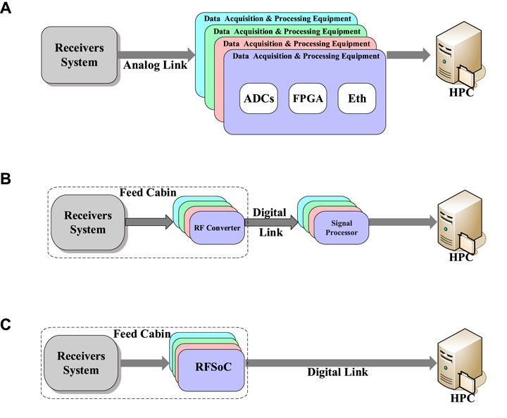
Figure 1. Astronomical backend system architecture. Earlier digitization and higher integration have been the main trends of telescope backend systems for digital signal processing in radio astronomy. (A) Implementation scheme of the traditional astronomical backend based on discrete data acquisition and processing equipment. (B) Implementation scheme of astronomical backend based on direct RF sampling. (C) Implementation scheme of astronomical backend based on RFSoC.
RF Direct sampling (RFDS) is the trend in backend design (Liu et al., 2021). It reduces the analog process by earlier digitizing RF signals while addressing the above issues. The RF converter at the receiver directly samples the RF signal and transmits it to the remote signal processor via the digital link, as shown in Figure 1B. This necessitates digital devices to feature smaller sizes, higher integration, and lower power consumption to accommodate narrow feed cabins and minimize electromagnetic interference to analog devices. As an early attempt to apply RFDS, MkI (Hotan et al., 2014) was equipped with 112 Xilinx Virtex-6 FPGAs and 192 ADCs. It operates exceeding 1 kW. The strong electromagnetic radiation and heat dissipation during high-power operations have always existed. Subsequently, NRAO has developed specialized miniaturized low-power analog-to-digital-to-optical modules to directly sample the receiver’s RF signals and transmit them via single-mode fiber links (Morgan et al., 2017). As a customized electronic system with no subsequent upgrades, its bandwidth is restricted to 311 MHz, and the data transfer rate caps at 2.5Gbps. Parks UWL (Hobbs et al., 2020) places RF-ADCs in the feed cabin and transmits the data to the FPGA via fiber optic based on the JESD204B interface protocol for massive data stream alignment and synchronization. Its data transmission rate is limited to 12.5 Gbps and must consider the additional power consumption, complex circuits, and driven clocks due to the protocol. These technologies, limited by the electronics industry development, restrict their application on the new generation backend represented by the QTT, which requires higher sampling bandwidth and data transfer rate while increasing the difficulty of updating iterations and general firmware development.
The advent of RFSoC realized the integration of high-performance, complete RF links. As the latest hardware platform of Xilinx ZYNQ series, RFSoC innovatively integrates high-performance RF data converter (RFDC) on the system-on-chip (SoC) (Xilinx, 2022). Highly integrated RFSoC will significantly reduce digital devices’ volume and power consumption to reduce electromagnetic interference to the analog front-end. It enables RFSoC to configure the complete RF link (Xilinx, 2019a) in the feed cabin, from RF digitization to processing, as shown in Figure 1C. Its on-chip data transmission rate is also up to 100Gbps. Moreover, as a commercial general-purpose chip, its rich and highly integrated development environment will significantly simplify firmware development and shorten the development cycle.
As the exploration of the QTT backend development, this paper builds a real-time baseband backend experimental system centered on RFSoC, combined GPU. The RFSoC-based RF pre-processing front-end is used to directly sample the RF signal, pre-process, package, and transmit by the on-chip 100GbE Interface. The raw baseband data packets, which are not integrated, can be utilized in research across various scientific domains, such as spectral line, pulsar, transient, VLBI, and Phased Array Feed (PAF). The GPU server receives packets via the digital optical fiber. It processes massive data in real-time, relying on powerful parallel computing capabilities and software-level flexibility. The radio spectral line observation has been conducted at the Nanshan 26-m radio telescope (NSRT) to verify its performance and our design concept. The RFSoC + GPU heterogeneous design provides a flexible, easy-to-cluster, and scalable solution for QTT backend implementation based on the full RF link. Moreover, this paper formulates the QTT backend scheme based on multiple RFSoC boards and computing nodes.
2 RFSoC review
RFSoC is currently the only adaptive RF platform in the industry. Based on the ZCU111’s ZXCU28DR RFSoC chip, this chapter overviews the function and advantages of such emerging hardware. The ZCU111, Xilinx’s evaluation board based on ZXCU28DR, is 30 cm high, 20 cm wide, and 0.2743 cm thick. The operating environment temperature ranges from 0°C to 45°C. The ZCU111 ensures RFSoC’s efficient heat dissipation based on the Infineon MAX6643 fan controller (Xilinx, 2018), improving the reliability of RFSoC operation under probable high resource utilization. It supports boot-up via SD card, QSPI, and JTAG interfaces. ZCU111 provides flexible data read-write and storage methods by featuring a 4 GB 64-bit SODIMM PS DDR4 memory and four 4 GB 64-bit PL DDR4 memory components and providing an M.2 SATA connector, an SD card slot, and two QSPI interfaces for high-speed access to external FLASH memory. The ZCU111 also features a USB 3.0 interface, an RJ45 interface, and four SFP+ interfaces to communicate and interact with the client-server. Additionally, it offers FMC-HPC, PMOD, and RFMC connectors for expanding peripheral circuits. Rich interfaces, peripherals, and Xilinx’s powerful testing environments make ZCU111 an ideal platform for validating concepts and developing and testing complex systems. The ZXCU28DR applied to the ZCU111 has a footprint identification of G1517, package dimensions of 20 mm
2.1 Review and evaluation of RFDC
RFDC is the core component of RFSoC. It includes eight high-performance RF-ADCs and RF-DACs. In radio astronomy, RF-DAC can provide test signals for receiver calibration (Liu et al., 2021), while RF-ADC will digitize RF signals in the backend design. Its sampling rate is up to 4.096 GHz, and the resolution is 12-bit. The integrated RFDC eliminates the need for external I/O in traditional discrete devices, which reduces the complexity of routing clocks and synchronizing all links in RFSoC-based PCB board design and avoids the large number of clocks required for driver interfaces in JESD204B protocol transmission. It will simplify system design, improve generality, and give RFSoC significant advantages over discrete devices in miniaturized low-power astronomical backend design. The Origin Space Telescope (OST) has verified the feasibility of replacing four dual-AD-DA-channel PCB boards operating at 30W with one RFSoC(Bradley et al., 2021). Compared to discrete devices, the operation power of dual 8-channel entire bandwidth will be reduced from 36W to 9W (Xilinx, 2019a). It will better limit electronic interference during the operation of the RFSoC digital devices (Pei et al., 2022).
Digitization is essential for backend devices, and this paper evaluates the innovative RFDC’s digital performance. Its sampling rate is set to 4096 MHz. The SMA110B-101624 signal generator will provide the test signal. The sampled data will be stored in the BRAM-based 16384-point snapshot block.
Firstly, we evaluated the spurious-free dynamic range (SFDR) of the RFDC. As the critical specification in data acquisition, SFDR measures the ADC’s available dynamic range when the fundamental signal is not disturbed or distorted by spurious components. The 5dBm test signals range from 100 MHz to 1900 MHz with intervals of 200 MHz. Figure 2A shows the SFDR and the fundamental signal power after digitization of Tile0’s two RF-ADC channels in different frequencies. After digitization, since each RF-ADC has its dedicated high-performance input buffer (Xilinx, 2019b), it experiences some attenuation that increases with frequency. The two channels’ SFDR is from 74dBFs to 83dBFs. It is sufficient to meet the digitization needs of most astronomical backend systems.
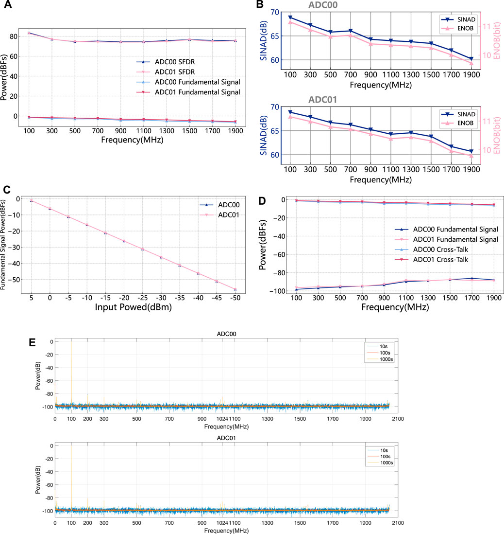
Figure 2. RFDC digitization performance evaluation. (A) The fundamental signal power and SFDR of Tile0’s two RF-ADCs in different frequencies of 5dBm. (B) The SINAD and ENOB of Tile0’s two RF-ADCs in different frequencies of 5 dBm. (C) Fundamental signal power under linear attenuation of test signal strength. (D) Cross-talk between two RF-ADCs of Tile0 at different frequencies of 5 dBm. (E) Stability testing of RFDC over time.
Then, this paper evaluated the signal-to-noise and distortion (SINAD) and effective number-of-bits (ENOB) of RFDC based on the sampling points for calculating SFDR. SINAD is the critical parameter for measuring the ADC’s overall dynamic performance. It reflects the noise and spuriousness within the Nyquist bandwidth. The higher SINAD indicates the lower the proportion of noise and spuriousness in the input power. ENOB, in bits, is used to assess the ADC’s conversion quality over the Nyquist bandwidth relative to the actual input signal. It has a linear relationship with SINAD. Figure 2B shows the two channels’ SINAD and ENOB at different frequencies. SINAD decreases with frequency, corresponding to the influence of the fundamental signal power with frequency in Figure 2A. For the ENOB across the entire bandwidth, ADC00 decreased from 11.1509 bits to 9.7169 bits, and ADC01 decreased from 11.151 bits to 9.7942 bits, each reducing less than 1.4 bits. Compared to most 8-bit ADCs in the current astronomical backend, RFDC will provide a sufficient dynamic range.
Due to the RFDC’s insertion and transmission track loss (Xilinx, 2019b; Liu et al., 2021), it is crucial in practical observations whether the power after digitization remains linear with the input signal strength. To this end, the signal generator provides a 100 MHz test signal and attenuates from +5dBm to −50dBm with intervals of 5dBm. As shown in Figure 2C, for Tile0’s two channels, the power of the digitized fundamental signal maintains a good linearity with the attenuation of the test signal.
One of the advantages of RFSoC is that RFDC’s multiple RF-ADCs can work simultaneously. Therefore, inter-channel crosstalk must be considered, especially for two RF-ADCs of the same tile. For this reason, we tested the crosstalk based on Tile0. The approach involves the signal generator delivering the 5dBm test signals range from 100 MHz to 1900 MHz with intervals of 200 MHz to ADC00 and measuring the power of this frequency coupled into ADC01 and vice versa. The test results are shown in Figure 2D. The power coupled to ADC01 shows an increasing overall trend with frequency, with all coupled powers below −80 dBFs. The crosstalk generated by ADC01 towards ADC00 also has the same trend.
Astronomy backend systems typically improve the SNR by integrating the observed weak signals, which necessitates the ADC to remain stable over time. The signal generator provides the 5dBm test signal with 100 MHz for RFDC and randomly selects 100 16384-point blocks each second to perform spectral accumulations of 10s, 100s, and 1000s for testing the RFDC’s stability. Figure 2E shows the amplitude response of two channels in Tile0. As the integration time increases, the background noise gradually smooths, its amplitude tends to be around −98.5 dB and the SNR increases. The weak 100 MHz signal’s harmonic interference and 512 MHz interleaving spurs, which gradually appear with increasing integration time but are consistently below −80dB, confirm the excellent performance and stability of RFDC under long-term operation.
2.2 Programmable logic and processing system
The programmable logic (PL) submodule is mainly used to implement the DSP and firmware logic. It inherits the Xilinx-7 series FPGA architecture, integrates rich LUT, and registers resources. Table 1 shows the key hardware parameters of monolithic RFSoC, SKAARB, and ROACH2. The latter two separate digital devices are widely used in astronomical digital backends. Table 1 shows that the on-chip feature-rich RFSoC has FPGA resources comparable to mainstream discrete digital devices. It offers the RFSoC the DSP capabilities required by the astronomical backend. In addition, it will reduce power consumption further and increase DSP capabilities by avoiding the resource consumption of interface protocols between different types of chips.
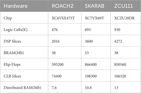
Table 1. FPGA resources for RFSoC, SKARAB, and ROACH2. ROACH2 is the FPGA-based reconfigurable open architecture computing hardware board developed by CASPER. It is the core of the FAST backend and DIBAS. The SKARAB, an upgrade to the ROACH2, is the latest discrete digital equipment launched by CASPER.
For processing system (PS), it comprehensively integrates processors, memory controllers, and common peripherals. It is interconnected with PL through the Advanced eXtensible Interface (AXI) bus. Its processor consists of an Application Processing Unit (APU) with a quad-core Artex Cortex-A53 and a Real-Time Processing Unit (RPU) with a dual-core Arm Cortex-R5F. Compared to the off-chip PowerPC for ROACH2, on-chip PS has the absolute size and power consumption advantages. Compared to the embedded IP softcore MicroBlaze for SKARAB, PS configuration is more straightforward and far superior in functionality, performance, stability, and development ecology. In this paper’s real-time baseband processing backend design, the PS will execute user applications on Linux systems running on APU. It will load and initialize PL firmware programs through the gigabit interface and interact with the client.
3 Materials and methods
In this paper, the real-time baseband processing backend consists of an RF pre-processing front-end and a data processing backend, and Figure 3 shows its system architecture. The ZCU111-based RFSoC RF signal pre-processing front-end achieves the complete RF signal link, including RF signal digitization and parallelization, pre-processing, data packing, and transmission based on the fixed-point operation. The firmware programs for these functions will be developed and compiled based on CASPER tool flow software (Hickish et al., 2016). The data processing backend is based on the server cored on the RTX3090 GPU to receive and process baseband packets in real-time. It reduces the coupling of two core components and provides exceptionally high flexibility. In this paper, the GPU server will post-process baseband data based on spectral observation requirements. The firmware parameters of the RF pre-processing front-end and the GPU program parameters can be adjusted according to different receiver types and observation needs in the future, so this will be a flexible and general backend design mode.
3.1 Parallel data generation subsystem
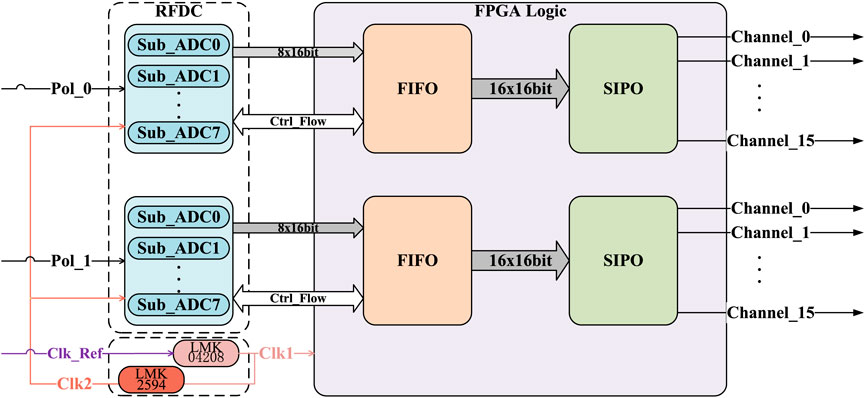
The parallel data generation subsystem is used for RF sampling and channelization output and provides clock support for the RFSoC. It consists of a time-interleaving sampling submodule, FPGA-based serial-in-parallel-out (SIPO) logic, and a clock submodule, as shown in Figure 4.
First, the RFDC-based time-interleaving sampling submodule digitizes RF signals directly. The RFDC’s ADC part contains four available independent tiles. In this paper, we select Tile0 and calibrate the sampling offset through the calibration mode provided by the RFDC to form two time-interleaving sampling submodules composed of eight sub-ADCs. They will digitize two polarized signals. Set the sampling rate to 2048 MHz, generate a serial data flow of eight 16-bit samples per clock cycle, and input the data into subsequent FPGA logic.
Next, FPGA logic receives the serial data flow using a first input first output (FIFO) with an output data width of 256-bit to reduce the difficulty of processing high-speed data of each parallel channel. The FIFO’s writing clock keeps synchronizing with the RFDC’s sampling clock, and the FIFO’s write enabling is controlled through the control signal flow to prevent the FIFO from being full or empty. The FIFO’s reading data keeps synchronizing with the FPGA logic, and the reset and read enabling can be set by the client-server. The FIFO’s output is a serial data flow composed of 16 16-bit data, and each channel’s data bandwidth processed by FPGA is reduced to 128 MHz. It improves the redundancy of FPGA in subsequent pre-processing. The 256-bit serial data flow will enter the 16-channel SIPO logic based on FPGA, which separates each sub-data in the way by slicing and outputs it from the corresponding channel according to the strict sequential relationship. Thus, it realizes the output of the dual 16-channel parallel data flow. The data rate of each channel is 1/16 of the input side of the FIFO.
Last, the clock module comprises LMX04208 and LMX2594 clock chips on the ZCU111 (Xilinx, 2020). It is configured by the clock file containing the register parameters generated by the Texas Instruments Clocks and Synthesizers (TICS) pro software. The external 10 MHz reference signal is first input into the LMK04208 clock chip and outputs the 256 MHz clock. It will drive the FPGA part and be fed into the LMK2594 clock chip, which will double to 2048 MHz as the sampling clock of the RFDC.
3.2 Data pre-processing subsystem
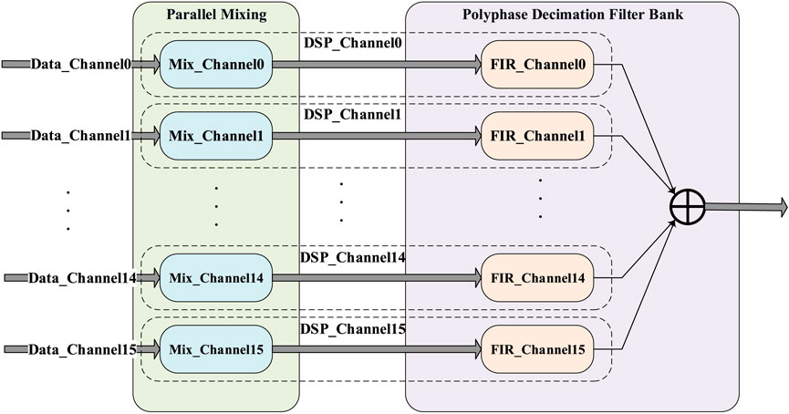
Baseband data is difficult to transmit directly and post-process in real-time because of its massive amount and very high data rate. Therefore, in the data pre-processing subsystem, we combine the parallel mixing and polyphase decimation filter bank (PDFB). It includes two of the same pre-processing modules, as shown in Figure 5, for simultaneous pre-processing of two polarization signals. The dual-16-channel parallel data stream generated by the parallel data generation subsystem is received and processed by the corresponding DSP sub-channels in each pre-processing module and converted into baseband data with a center frequency of 256 MHz and a bandwidth of 100 MHz.
The data pre-processing subsystem, especially the PDFB, will consume the most FPGA resources. Therefore, this paper reduces the order of each channel by half through the linear phase characteristic of the finite impulse response (FIR) filter to reduce the excessive consumption of FPGA resources. For an N-order even-symmetric linear phase FIR filter commonly used in low-pass and bandpass designs, its frequency response is shown in Eq. 1,
which requires its unit impulse response coefficient h(n) to meet the characteristics shown in Eq. 2.
After converting into the D-channel polyphase structure, each channel corresponds to a Q-order impulse response, and the product of Q and D equals N. According to Eq. 2,
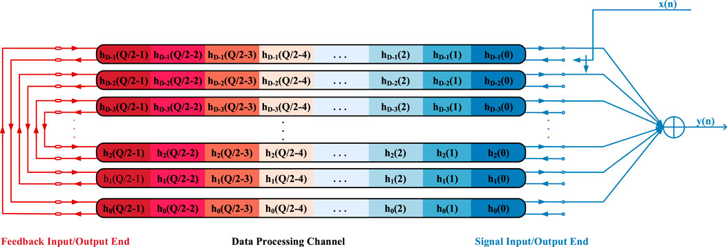
Since half of the coefficients and logical resources in the i-th and D-1-i-th channels can be reused, based on the reusable structure shown in Figure 6, each sub-channel is halved in length by receiving half-processed feedback data and outputting processed data.
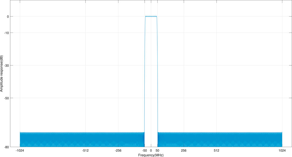
In this system, we provide a data bandwidth of 100 MHz based on the 672-order equiripple low-pass filter. Its coefficients are symmetric, and its amplitude response is shown in Figure 7. We combined reusable and non-reusable structures PDFB with parallel mixing to build a pre-processing module. Then, we compared the hardware resource consumption and proportion under two modes, as shown in Table 2. Among them, synthesis and implementation correspond to converting the design into a gate-level netlist, and placement and routing the gate-level netlist, respectively. In the pre-processing module based on reusable structure, the occupancy rate of hardware resources such as LUT, FF, and DSP, which participate in operations, significantly decreases. Less resource consumption reduces power consumption during operation. Compared to non-reusable structures, the single reusable structure reduced its on-chip power from 9.205W to 8.264W. Among them, dynamic power was reduced from 7.949W to 7.02W, and static power was reduced from 1.255W to 1.244W.
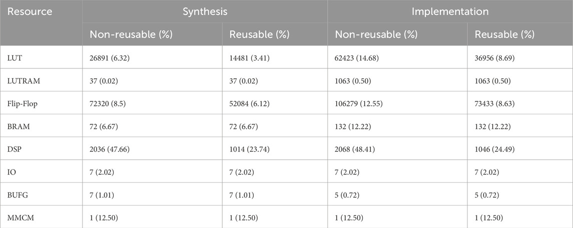
Table 2. Resource utilization of reusable and non-reusable structures single polarization pre-processing.
3.3 High-speed ethernet transmission subsystem
First, the FPGA-based packet data generation module will combine two pre-processed polarized signals to synthesize a 256-bit serial data flow, as shown in Figure 8A. Next, it is divided into four 64-bit data through the slicing logic and transmitted successively by the multiplexer to the data packaging module. Each 64-bit data contains two dual-polarization complex data of consecutive moments, and their real and imaginary parts are divided, as shown in Figure 8B.
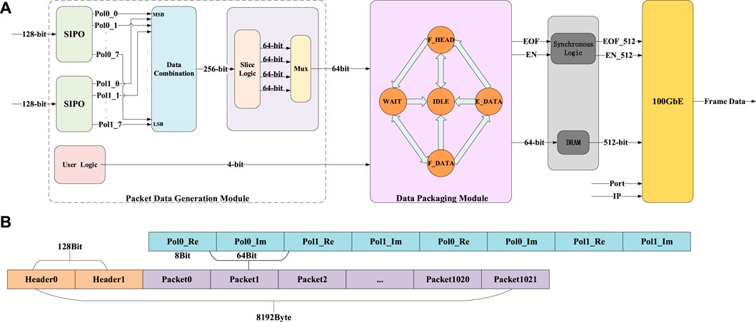
Figure 8. The processing and packaging process, signal flow of the high-speed Ethernet transmission subsystem. (A) Block diagram of high-speed Ethernet transmission subsystem firmware. (B) Single frame data structure.
Secondly, the data packaging module centers on the finite-state automaton (FSM) based on FPGA logic. The FSM defines five states: IDLE, F_HEAD, F_DATA, E_DATA, and WAIT. According to the different FSM control flags, transitions between states are implemented to perform corresponding firmware logic functions, as shown in Figure 8A. The FSM outputs the packets and the 100GbE Interface control signal stream containing EN and EOF. For the 100GbE Interface, the EN is the data received enable flag, and the EOF is the frame end data flag for determining the frame length. Initially, FSM jumps from the initial IDLE to the F_HEAD. It receives the 4-bit user-defined data flow that can be empty and combines it with the counter only running in this state to form two 64-bit frame header packets and outputs it. Then, FSM cycles repeatedly in the WAIT and F_DATA to wait for data and output packets. Eventually, after outputting 1022 packets, the FSM jumps to the E_DATA, outputs the EOF-enable signal to form a frame of 1024 packets, and re-enters F_HEAD. All states can be transmitted to the initial IDLE state through the reset signal. Another control signal flow, EN, remains enabled in the F_HEAD and F_DATA.
Finally, to match the 512-bit input port of the 100GbE Interface, the 64-bit packets output by FSM first pass through the random access memory (RAM). The RAM is composed of block RAM(BRAM) resources to achieve simultaneous transmission of eight packets. The control flow signals EN and EOF output by FSM also need to input FPGA-based synchronization logic to reach clock synchronization with 512-bit data. The client-server provides the IP address and port number to the Ethernet ports through software registers for sending data to the specified GPU server.
3.4 Data processing backend
GPU and Compute Unified Device Architecture (CUDA) technologies have been well applied in radio astronomical signal processing. With the powerful computing resources of high-performance GPUs, real-time post-processing of massive data generated by the RF pre-processing front-end has become possible.
In the real-time baseband post-processing backend, the main hardware of the GPU server includes an Intel Xeon E5-2603 CPU, 64 GB of memory, and 8 TB of SSD storage. In the experiment, we selected NVIDIA GeForce RTX 3090. This powerful GPU supports the second-generation RTX architecture and has 10496 NVIDIA CUDA cores, 24 GB global memory, high clock speed, and faster running speed.
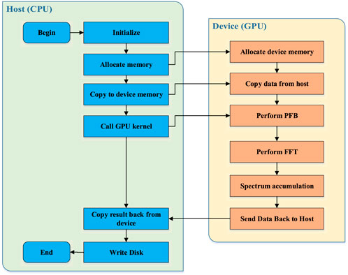
The GPU server receives baseband packets through the Network Interface Card (NIC) and processes them in real-time. Due to the massive amount of data and high data rate, it cannot be directly sent to the GPU device for processing. To improve packet capture efficiency and read-write rate, we built a flexible and manageable temporary ring buffer based on CPU memory to cache and distribute the received UDP frame data for GPU processing in real-time. We developed GPU programs based on the CUDA programming model on the GPU server. It is divided into the GPU’s parallel device program and the CPU’s serial host program to realize data-intensive tasks and logic control, respectively. Its design flow is shown in Figure 9. First, the host program initializes the variables, selects the CUDA device, allocates memory space for filter coefficient and data array on the CPU and GPU, and copies to the GPU global memory. Next, the GPU kernel function runs the device program based on floating-point operations. The parallel 8-tap Polyphase Filter Bank (PFB) algorithm is first performed. It converts the serial channelization process into multi-channel parallel processing, efficiently achieving sub-band division of baseband data. The 32768-channel and 131072-channel modes correspond to channel spacing of 3.051 kHz and 0.763kHz, respectively, with equivalent noise bandwidth (ENBW) of 2.497kHz and 0.599 kHz. The parallel FFT algorithm and subsequent spectrum accumulation operation are performed according to the processing results. Finally, the CPU copies the GPU kernel’s processing results into the CPU memory and writes it to the local disk.
4 Result
4.1 Experimental environment test result
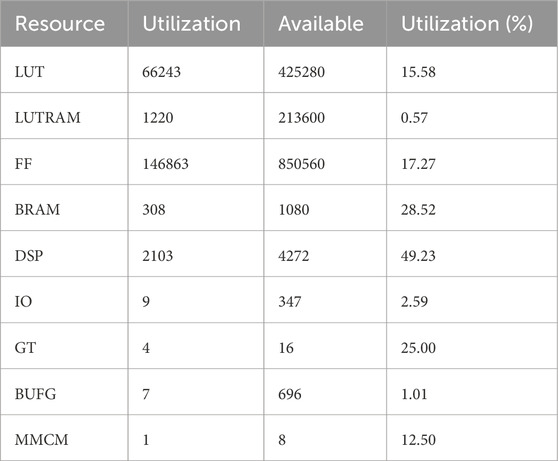
Before testing the system performance, we checked the hardware resource usage of the RF pre-processing front-end after implementation, as shown in Table 3. Comparing the single pre-processing module’s usage after implementation in Table 2, the subsystem for pre-processing the two polarization signals consumes the most hardware resources.
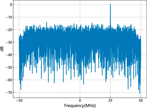
Firstly, one frame of data that the GPU server has not processed is analyzed in its spectrum to verify the correctness of the RF pre-processing front-end design. SMA110B-101624 signal generator, as the RF signal source, is required to provide a high-power signal, and we set it up at −40 dB. The GPU server will capture the only pre-processed 8192-byte data frame of the RFSoC front-end and perform offline operations involving removing the frame header’s two 8-byte packets to extract the 8176-byte data part, followed by executing a 32768-point FFT and FFTSHIFT to analyze its amplitude response. After RFSoC front-end mixing and filtering, the spectrum of the RF test signal from 306 to 206 MHz will be shifted from −50 to 50 MHz. The center frequency of 256 MHz will be shifted to 0 MHz, the 306 to 256 MHz will be shifted to −50 to 0 MHz, and the 256 to 206 MHz will be moved to 0–50 MHz. Out-of-band signals below 206 MHz and above 306 MHz will be filtered out. Figure 10 shows the amplitude responses of 231 MHz RF test signals after pre-processing, and the frequency point corresponds to the positions of 25 MHz in the passband. It is in line with the design logic of the RF single acquisition front-end.
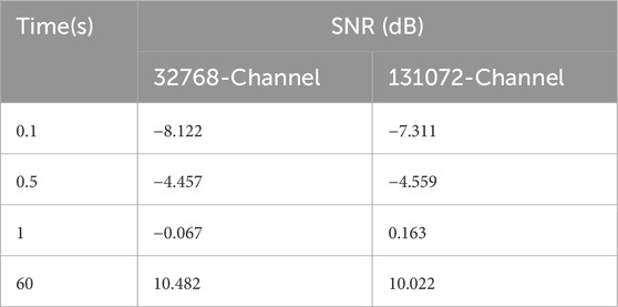
Then, the signal generator provides the −90 dB low-power test signal, and we analyze its amplitude response after the GPU server completes the real-time post-processing for the specified duration to ensure the system’s overall performance. First, the packet was captured and post-processed in real-time for 0.1s, 0.5s, and 1s in two modes with 32768 and 131072 channels. Their amplitude response corresponded to the first three subgraphs of Figures 11A, B, respectively, and the frequency resolution corresponds to 3.051kHz and 0.763 kHz. With the increased processing time, the low-power RF signal can be recovered. Among them, the 231 MHz signals’ amplitude responses under different processing durations are accurately located at 25 MHz within the bandpass, respectively. With the increase in processing time, the background noise amplitude tends to converge to the middle and decreases. The signal-to-noise ratio (SNR) also improves, as shown in Table 4. The DC signal can also be shown with the rise in the processing time. Next, we conducted a 1-min real-time data processing on the two modes, respectively, and no data was lost by analyzing each data’s frame header. The amplitude responses are shown in the fourth subgraph of Figures 11A, B, respectively. With increasing processing time, the passband’s amplitude response more closely resembles the contour of the equiripple low-pass filter shown in Figure 7. It proves the realization and design correctness of the system’s overall function.
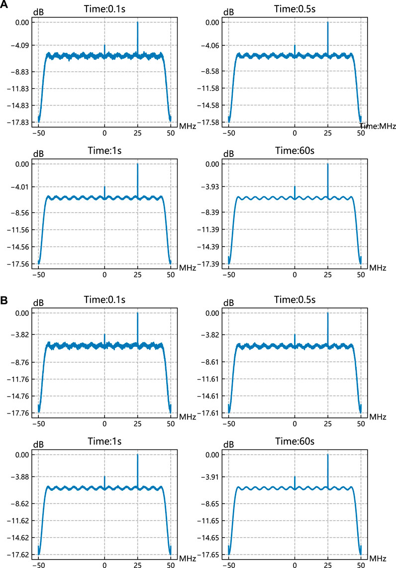
Figure 11. System overall testing based on low-power test signals. (A) The amplitude response of the 231 MHz RF input signal processing at 32678-channel mode for different times. (B) The amplitude response of the 231 MHz RF input signal processing at 131072-channel mode for different times.
4.2 Observation experiment result
The real-time baseband backend has carried out observation tests with the NSRT and demonstrated its performance by successfully observing the absorption lines of H2CO molecules from the massive star-forming region in the C-band. The ZCU111 is installed in the radio telescope system and observed by the C-band dual-polarization receiver in the 4–8 GHz by adjusting the local oscillator (LO). The dual polarization signals from the telescope’s cryogenic receiver are fed to Tile0’s ADC0 and ADC1, with 2048 MHz sampling and a 12-bit resolution.
First, the LO frequency of the receiver is set to 4550 MHz. The observation coordinates (J2000) are set to 02:25:29.24, 62:05:55.60. The observation mode adopts position switching mode, and the time of ON SOURCE and OFF SOURCE take 3 min to obtain real-time processed observation data and record it in Fits file format. Next, flow and frequency calibration are performed on the observed data, combined with the information on antenna position, antenna efficiency, and atmospheric opacity, and are analyzed by GILDAS software. Figures 12A, B show the processing results of the 32768-channel and 131072-channel observation modes, respectively. The Y-axis represents the noise temperature, the unit is K, and there are two horizontal axes: speed and frequency. It can be seen that compared to Figures 12A, B has a significant improvement in frequency resolution, and their design index corresponds to 3.051kHz and 0.763 kHz. Both the speed of peak flow is −40 km
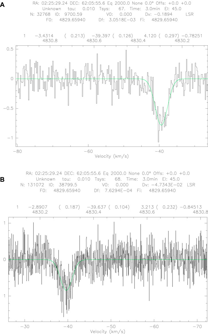
Figure 12. System observation test based on the NSRT. (A) H2CO absorption line at 3.051 kHz frequency resolution under 3-minute observation. (B) H2CO absorption line at 0.763 kHz frequency resolution under 3-minute observation.
5 QTT baseband backend system construction planning
The RFSoC RF pre-processing front-end combined with GPU real-time computing nodes provides a flexible and scalable software-hardware solution for future QTT general backend design. Based on the abovementioned solutions, we develop the backend system design scheme for the first phase project of the QTT receiver system, currently under construction.
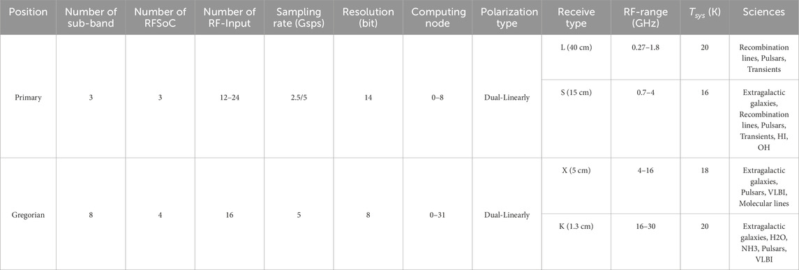
Firstly, the first phase will design and install four different receivers. The L-band and S-band receivers will be installed at the main focus, and the X-band and K-band receivers will be installed at the Gregorian focus for 0.27GHz–30 GHz observation frequency coverage. As shown in Table 5, they will satisfy the observation requirements of multiple scientific fields, such as pulsars, transients, extragalactic galaxies, and spectral lines. Since the two focuses’ physical locations are far apart, the main and the Gregorian focus will each install a set of RFSoC RF pre-processing front-end systems. Two receivers share a set of systems through the multiplexer.
Next, telescope receivers with extremely high sensitivity are more susceptible to RF interference when detecting weak radio astronomical signals, particularly for UWB receivers, where passband interference inevitably increases with bandwidth. To avoid the saturation effect of interference on the receiver’s RF signal acquisition link, the main focal point’s low-band receivers and the Gregorian focal point’s high-band receivers will divide the RF signal into three and eight analog subbands, respectively. In addition, the QTT backend will feature RFI reference channels for future 13-m reference antennas (Wang et al., 2023) to be established near the QTT for mitigating RFI. For the receivers based on dual-linear polarization, it will generate 12 and 32 analog subband signals, respectively, at the main and Gregorian focus points. Considering the cost, equipment size requirements, and RFSoC data transmission capability, the main and Gregorian focus points’ RFSoC pre-processing front-end will comprise three and four RFSoC boards, respectively. Through the multiplexer, they will select six and eight analog sub-bands for digitization, processing, packaging, and transferring to the 100G switch network. Based on the FMC+ interface, each board will expand to two 100GbE Interfaces. As shown in Table 5, based on observation tasks and analog sub-band bandwidth, the main focus’s RF pre-processing front-end will directly digitize with three modes: 2.048Gsps, 2.56Gsps, and 4.096Gsps. The resolution is 12-bit, and the data rate for the RFSoC board with dual 100GbE Interface is 65.536Gbps, 81.92Gbps, and 131.072Gbps, respectively. The Gregorian focus’s RF pre-processing front-end will digitize wider subbands with 4.096Gsps and reduce the data rate and volume with 8-bit resolution. The data rate for each RFSoC board is 131.072Gbps.
Finally, based on the real-time post-processing mode proposed in this paper, we plan to set up 32 GPU computing nodes in the signal processing room at the far end of the feed cabin. As shown in Table 5, nine computing nodes will participate in real-time data post-processing of the main focus. They will also combine with another 23 computing nodes for real-time data post-processing of the Gregorian focus. Based on the IP and port number set by the client-server, the 100GbE Interface’s baseband packets will be routed to the designated computing node and processed according to the specified observation requirements. For example, in the pulsar observation, GPU servers will run corresponding programs in real-time for the baseband data, which has been pre-processed, coarse channelized, and packaged by RFSoC, such as PFB, dispersion removal, folding, integration, and the pulsar search algorithm. Transient observation focuses on detecting fast radio burst (FRB) signals, which have extremely short duration, high flux, and similar spatial dispersion phenomena to pulsars. Therefore, for the new FRB detection, GPU computing nodes with a large computation will try dispersion removal based on a wide range of dispersion measures (DM). The design offers flexibility and convenience for backend expansion and upgrading, allowing it to adapt to unknown scientific exploration and future receiver design planning for the QTT.
6 Conclusion
Giving attention to both the system’s generality and flexible and efficient digitization, processing, and transmission of increasingly massive ultra-wideband observation signals are the development trends of the new generation’s astronomical backend, including QTT. Based on the abovementioned requirements, this paper attempts to apply RFSoC-based configurable full RF links to backend design. Many experimental tests have been carried out in the laboratory, and the system’s performance was proved by radio spectral line observation on the NSRT. It can be applied to different radio telescope platforms independently and also integrated into QTT’s backend system in the future, with good generality.
The RFSoC-based QTT backend offers a completely configurable RF link solution with a compact size, low device count, and low power consumption. By eliminating the need for external high-power, large-volume ADC and processor modules, two RFSoC boards can be easily placed in one 1U standard chassis, which usually only accommodates one mainstream data collection and processing equipment such as ROACH2. In addition, RFSoC, which simultaneously supports up to eight-channel RF digitization with 4.096Gsps, will reduce the number of devices and significantly improve work efficiency compared to mainstream equipment. For example, to digitize and process subbands, the DIBAS, VEGAS, and FAST backends require three, eight, and twelve data acquisition and processing equipment that only support dual-channel maximum sampling. Additionally, RFSoC’s 100GbE Interface is more suitable for the high data transmission needs of future UWB receivers compared to the 10GbE and 40GbE Interfaces widely used in astronomical backends.
The proposed real-time baseband data processing mode of RFSoC + GPU provides fresh ideas for developing the new generation’s backend system in this paper. The RFSoC RF pre-processing front-end at the receiver and the remote end’s GPU server will load and run the corresponding RFSoC firmware and GPU programs according to different observation targets. It has high flexibility and is easy to extend and upgrade. We can conveniently add new firmware designs and enrich work modes according to the demand for QTT receiver subband planning and observation in the future. We will continue to design and develop multi-subband multipath transmission and multi-scientific object processing based on multi-GPU computing nodes. In addition, this paper explores the application of RFDC and 100GbE Interface on astronomical digital backends. The firmware design based on them for parallel data generation and 100GbE Ethernet transmission can be considered a standard general design. The corresponding data pre-processing logic can be constructed according to actual observation needs.
In future work, we will combine the ZCU111’s usage experience in this paper with the QTT’s requirements to design radio astronomy-dedicated RFSoC RF pre-processing front-end boards. We will continue exploring synchronization design between multiple RFSoC boards, RFSoC shielding, and heat dissipation design.
Data availability statement
The raw data supporting the conclusions of this article will be made available by the authors, without undue reservation.
Author contributions
Q-SZ: Data curation, Methodology, Software, Writing–original draft, Writing–review and editing, Conceptualization, Formal Analysis. M-ZC: Conceptualization, Data curation, Formal Analysis, Funding acquisition, Supervision, Writing–review and editing. JL: Conceptualization, Data curation, Formal Analysis, Funding acquisition, Supervision, Writing–review and editing.
Funding
The author(s) declare that financial support was received for the research, authorship, and/or publication of this article. This work was supported by the Light in China’s Western Region program (2022-XBQNXZ-012) and the National Natural Science Foundation of China (Grant No. 12073067).
Acknowledgments
We thank the CASPER community for developing the ZCU111 libraries, Dalei Li for his help with data processing, and Jianping Yuan for their help in the NSRT 26 m observation. Finally, we thank the referees for taking valuable time and providing valuable feedback on the paper.
Conflict of interest
The authors declare that the research was conducted in the absence of any commercial or financial relationships that could be construed as a potential conflict of interest.
Publisher’s note
All claims expressed in this article are solely those of the authors and do not necessarily represent those of their affiliated organizations, or those of the publisher, the editors and the reviewers. Any product that may be evaluated in this article, or claim that may be made by its manufacturer, is not guaranteed or endorsed by the publisher.
References
Beresford, R., Cheng, W., Hampson, G., Bunton, J., Brown, A., Leach, M., et al. (2017). “Radio astronomy l-band phased array feed rfof implementation overview,” in 2017 XXXIInd General Assembly and Scientific Symposium of the International Union of Radio Science (URSI GASS), 1–4. doi:10.23919/URSIGASS.2017.8105423
Brown, A. J., Hampson, G. A., Roberts, P., Beresford, R., Bunton, J. D., Cheng, W., et al. (2014). Design and implementation of the 2nd Generation ASKAP Digital Receiver System, 2014 International Conference on Electromagnetics in Advanced Applications (ICEAA), 268–271.
Ford, J. M., Prestage, R. M., and Bloss, M. (2014). Experiences with the design and construction of wideband spectral line and pulsar instrumentation with CASPER hardware and software: the digital backend system 9152. 915218. doi:10.1117/12.2056883
Hampson, G., Roberts, P., Leach, M., Brown, A., Bateman, T., Neuhold, S., et al. (2015). “Microwave phased array digital beamforming system design challenges for ska,” in 2015 European Microwave Conference (EuMC), 710–713. doi:10.1109/EuMC.2015.7345862
Hickish, J., Abdurashidova, Z., Ali, Z., Buch, K. D., Chaudhari, S. C., Chen, H., et al. (2016). A Decade of Developing Radio-Astronomy Instrumentation using CASPER Open-Source Technology. Journal of Astronomical Instrumentation 5, 1641001–12. doi:10.1142/S2251171716410014
Hobbs, G., Manchester, R. N., Dunning, A., Jameson, A., Roberts, P., George, D., et al. (2020). An ultra-wide bandwidth (704 to 4 032 mhz) receiver for the parkes radio telescope. Publications of the Astronomical Society of Australia 37, e012. doi:10.1017/pasa.2020.2
Hotan, A. W., Bunton, J. D., Harvey-Smith, L., Humphreys, B., Jeffs, B. D., Shimwell, T., et al. (2014). The australian square kilometre array pathfinder: System architecture and specifications of the boolardy engineering test array. Publications of the Astronomical Society of Australia 31, e041. doi:10.1017/pasa.2014.36
Liu, C., Jones, M. E., and Taylor, A. C. (2021). Characterizing the performance of high-speed data converters for RFSoC-based radio astronomy receivers. mnras 501, 5096–5104. doi:10.1093/mnras/staa3895
MA, J., PEI, X., WANG, N., LI, J., WANG, K., and LIU, Y. (2019). Ultra wideband and multi-beam signal receiving and processing system of qtt. SCIENTIA SINICA Physica, Mechanica and Astronomica 49, 099502. doi:10.1360/SSPMA-2019-0014
Morgan, M. A., Wunduke, S. D., Castro, J. J., Boyd, T. A., and Groves, W. (2017). “Compact cm-wave and mm-wave integrated receivers,” in 2017 XXXIInd General Assembly and Scientific Symposium of the International Union of Radio Science (URSI GASS), 1–4. doi:10.23919/URSIGASS.2017.8104501
Na-fei, W., Bin, L., and Qing-yuan, F. (2010). Design of fiber-optic link for broadband microwave signal transmission. Annals of Shanghai Astronomical Observatory Chinese Academy of Sciences, 54–61.
Pei, X., Li, J., Duan, X., and Zhang, H. (2023). Qtt ultra-wideband signal acquisition and baseband data recording system design based on the rfsoc platform. Publications of the Astronomical Society of the Pacific 135, 075003. doi:10.1088/1538-3873/ace12d
Pei, X., Wang, N., Werthimer, D., Duan, X.-F., Li, J., Ergesh, T., et al. (2022). Design of rfsoc-based digital phased array feed (paf) and hybrid architecture beamforming system. Research in Astronomy and Astrophysics 22, 045016. doi:10.1088/1674-4527/ac56cb
Stanko, S., Klein, B., and Kerp, J. (2005). A field programmable gate array spectrometer for radio astronomy - first light at the effelsberg 100-m telescope. A&A 436, 391–395. doi:10.1051/0004-6361:20042227
Roshi, D. A., Bloss, M., Brandt, P., Bussa, S., Chen, H., Demorest, P., et al. (2011). “Advanced multi-beam spectrometer for the green bank telescope,” in 2011 XXXth URSI General Assembly and Scientific Symposium, 1–4. doi:10.1109/URSIGASS.2011.6051280
Wang, N., Xu, Q., Ma, J., Liu, Z., Liu, Q., Zhang, H., et al. (2023). The Qitai radio telescope. Science China Physics, Mechanics, and Astronomy 66, 289512. doi:10.1007/s11433-023-2131-1
Keywords: astronomical backend, QTT, RFSoC, RF signal link, heterogeneous
Citation: Zhang Q-S, Chen M-Z and Li J (2024) General heterogeneous real-time baseband backend system scheme applied to QTT based on RFSoC+GPU. Front. Astron. Space Sci. 11:1420066. doi: 10.3389/fspas.2024.1420066
Received: 19 April 2024; Accepted: 27 June 2024;
Published: 20 August 2024.
Edited by:
Christophe Risacher, International Research Institute for Radio Astronomy, FranceReviewed by:
Carlos Frajuca, Federal University of Rio Grande, BrazilBernd Klein, Max Planck Institute for Radio Astronomy, Germany
Benjamin Quertier, UMR5804 Laboratoire d’astrophysique de Bordeaux (LAB), France
Copyright © 2024 Zhang, Chen and Li. This is an open-access article distributed under the terms of the Creative Commons Attribution License (CC BY). The use, distribution or reproduction in other forums is permitted, provided the original author(s) and the copyright owner(s) are credited and that the original publication in this journal is cited, in accordance with accepted academic practice. No use, distribution or reproduction is permitted which does not comply with these terms.
*Correspondence: Mao-Zheng Chen, Y2hlbkB4YW8uYWMuY24=
 Qing-Song Zhang
 Mao-Zheng Chen1,2,3*
