 Erik M. Tejero
 George Gatling
 Matthew C. Paliwoda
- Plasma Physics Division, US Naval Research Laboratory, Washington, DC, United States
Introduction: This work describes the calibration of a laboratory plasma impedance probe, a diagnostic to accurately measure the plasma density using resonances in the self-impedance spectrum that are introduced when the probe is immersed in a plasma. This paper focuses on calibration techniques that are essential for typical laboratory plasmas with resonant frequencies above 100 MHz, which corresponds to plasma densities above 108 cm-3 and have been used for plasma densities from 105 to 1010 cm-3 that are found in typical laboratory plasmas.
Methods: The approach uses a calibration circuit included in the measurement circuitry, along with careful characterization of the RF paths after the calibration plane to account for the parasitic impedances. The calibration algorithm is derived and an example step-by-step calibration is presented. Calibration procedures are validated with test loads, numerical simulations, and theoretical models.
Results: The calibration procedure successfully recovered the impedance of a test load with an average error of 1%. Using a full three-port balun model, the vacuum impedance of the dipole was accurately recovered. Plasma density measurements derived from the calibrated impedance spectrum agreed well with Langmuir probe measurements, while uncalibrated spectra resulted in significant overestimation of plasma density. Monte Carlo simulations demonstrated that using six calibration standards in the SOL calibration significantly improved the accuracy of the calibration coefficients and reduced error in the recovered test load impedance.
Discussion: The calibration procedure described in this manuscript provides accurate impedance measurements in laboratory plasmas, enabling reliable extraction of plasma parameters. The importance of accurate calibration is highlighted with high-frequency measurements using balanced dipole antennas as an example. The use of multiple calibration standards and the full three-port balun model significantly improves measurement accuracy.
1 Introduction
A plasma impedance probe uses measurements of the impedance spectrum for an antenna immersed in a plasma to infer plasma parameters. The presence of the plasma introduces resonances into the impedance spectrum that are not present when the antenna is in vacuum. The frequencies at which these resonances occur allow us to determine the plasma density (Balmain, 1964), plasma potential (Walker et al., 2010), and electron temperature (Bishop and Baker, 1972; Walker et al., 2008). The impedance spectrum can be calculated from measurements of the reflection coefficient,
The typical impedance probe analysis is valid for the antenna and plasma system, but does not account for the measurement circuitry, cabling, or parasitic impedances present in the system. The cumulative effect of these can result in shifting the frequencies of the resonances of interest or in the introduction of new resonances. For impedance probes used to measure space plasmas, the frequencies of interest are relatively low (less than 15 MHz) and calibration is typically performed by measuring a set of calibration standards across the antenna feed prior to final integration of the antenna (Young, 2020; Swenson et al., 2003). However, for laboratory plasmas instruments where we are required to measure in the GHz range, even an adapter or a length of transmission line on the order of 1 cm can cause errors of 60% or more (Brooks et al., 2023). For accurate plasma parameter measurements, it is essential that we develop techniques to mitigate these effects using modeling, calibration, and network de-embedding. Although it is clear that calibration is necessary for accurate plasma impedance probe measurements, it must also be approached with great care due to the ability to drastically change the impedance spectrum. A poorly calibrated probe can lead to errors of the same size or greater than an uncalibrated probe. For example, a simple circuit of a resistor to ground can have parasitic impedances yielding a resonant frequency. Proper calibration can eliminate the resonance and recover the largely ideal resistor impedance.
Similar techniques to those used to calibrate impedance probes measuring space plasmas have been used for laboratory plasma impedance probes (Blackwell et al., 2005; Bilén et al., 1999; Hopkins and King, 2014). These probes have typically used monopole antennas built using a short coaxial transmission line as the feed. These techniques work well as they provide a repeatable, well-defined connection for attaching calibration standards. However, the reference electrode for a monopole antenna is not well defined and can change due to interactions with the plasma. For this reason, we prefer to use dipole antennas for our impedance probes. The requirement of a balanced dipole antenna does not allow us to employ the simpler calibration techniques used previously.
The general approach that we take to calibration of a laboratory plasma impedance probe is based on the short-open-load (SOL) calibration (Kruppa and Sodomsky, 1971) and fixture de-embedding techniques making use of the transmission matrix (T-matrix) (Bauer and Penfield, 1974). However, the use of a balun to make a balanced dipole antenna in our impedance probe design requires us to de-embed a three-port network. The presence of the unbalanced port breaks the two-port symmetry on which the T-matrix de-embedding is based.
2 Materials and equipment
Our laboratory measurement electronics consists of an RF I-V measurement circuit and an on-board calibration circuit. Each of which will be described in detail below. The plasma impedance probe can be operated in two distinct modes. The first uses a VNA to provide the RF signal to the probe and measures the reflection coefficient for the network. In practice this provides excellent dynamic range for the measurement but acquisition times are limited by the Intermediate Frequency (IF) bandwidth setting of the instrument. The second uses a function generator to provide the stimulus and an oscilloscope to measure the current and voltage outputs from the RF I-V measurement circuit. The calibration procedures will be described using the RF I-V measurement method in the main text, and a description using a VNA will be described in the Supplementary Appendix.
The RF I-V method typically is used to measure impedances in frequency ranges from 1 MHz to 3 GHz. It provides better accuracy and a wider impedance range than the reflection coefficient method used by VNAs, (Keysight Technologies) when measuring impedances far from the characteristic impedance of the system
As the impedance gets large or very small, the reflection coefficient asymptotically approaches ±1 respectively, and exhibits the largest sensitivity at
The RF I-V measurement circuit consists of two RF transformers: one in series whose voltage on the secondary is proportional to the current and one in parallel to measure the voltage. Placing the voltage measurement in parallel with the series combination the current measurement and the dipole will reduce the accuracy of the voltage measurement. Conversely, placing the current measurement in series with the parallel combination of the voltage measurement and the antenna will reduce the accuracy of the current measurement. Since, the currents are expected to be small at the plasma frequency, we used the former arrangement with the current measurement directly in series with the antenna, as shown in Figure 1.
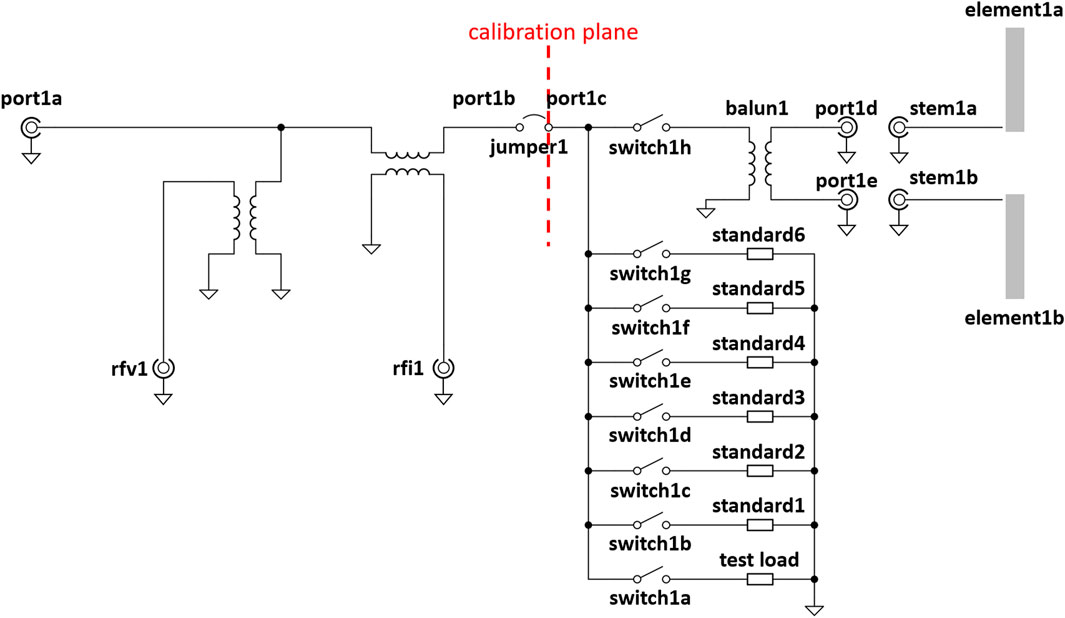
Figure 1. The RF I-V and on-board calibration circuit. A network of eight RF switches allows us to make measurements of a test load that is used to verify calibration, six calibration standards, and the dipole antenna. Red dashed line indicates the location of the calibration plane, which occurs at port1c. The remainder of the circuit is modeled using a combination of network characterization and idealized models.
The on-board calibration circuit was designed to allow for calibration of the impedance probe up to port1c, as indicated in Figure 1. It consists of an 8-channel RF switch that allows us to connect the RF I-V circuit to one of eight loads: a tank circuit test load that simulates the resonant behavior of typical laboratory plasmas, one of six calibration standards, and the dipole antenna. The test load is used to verify that an accurate calibration was made to port1c. When the impedance probe is installed in the SPSC, there is a significant length of cable between the RF source for the probe and the antenna. In addition, the main plasma source is a bank of hot tungsten filaments, where the infrared radiation can lead to substantial heating of the cables and other equipment. Calibrations conducted at room temperature at atmospheric pressure were observed to no longer be valid when the plasma source was in operation. This was the main motivation for the inclusion of the on-board calibration circuit.
Switch1h of the 8-channel RF switch is connected to the unbalanced side of a balun. The balanced ports are connected to two SMA bulkhead connectors labeled as port1d and port1e in Figure 1, which allow for accurate characterization of the 3-port network between port1c, port1d, and port1e. Then, two semi-rigid coaxial transmission lines, labeled stem1a and stem1b, form the feed of the dipole antenna, drawn in Figure 2. The shield and dielectric of the semi-rigid coaxial lines are cut back approximately 1.9 cm and 1.3 cm respectively. The 1.3-cm exposed center conductor is inserted into 1.3-cm diameter and 5-cm long aluminum rod, which serves as a dipole element.
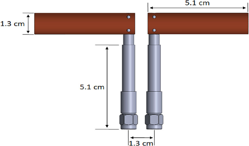
Figure 2. Drawing of the dipole antenna used for the plasma impedance probe. The dipole elements are hollowed out aluminum rods that are attached to the center conductors of the semi-rigid coax stems via set screws.
The probe was tested in the NRL Space Physics Simulation Chamber (SPSC), a large volume vacuum chamber used to replicate ionospheric and magnetospheric plasmas in the laboratory. It consists of two parts: a 0.55-m diameter, 2-m long source chamber section and a 2-m diameter, 5-m long main chamber section. The two sections are separated by a large gate valve that allows them to be operated independently or as a whole. The chamber is surrounded by 12 individually controlled, water-cooled electromagnets that can be used to generate arbitrary axial field shapes (Tejero and Gatling, 2009). Typical vacuum base pressure is 10–6 Torr. When in operation, the chamber is back-filled with Argon gas at operating pressures around 10–4 Torr. The hot filament plasma source in the main chamber can create plasmas with densities from 105 to 1010 particles per cm3. Uniform magnetic fields up to 200 G can be created in main chamber to confine the plasma, but it is typically operated with magnetic field values from 20 to 80 G. Under these conditions, a laboratory plasma impedance probe will need to sweep the drive frequency from approximately 1 MHz to 1 GHz.
3 Methods
Our approach to calibration is to first use measurements of the on-board calibration standards to conduct a 1-Port SOL calibration, which establishes our calibration plane at port1c shown in Figure 1. Then, we develop a general model for the network from port1c to the antenna as a function of the dipole impedance. The model incorporates measured characterization of the balun and ideal models of the stems. Then, we use a nonlinear fit of the dipole measurement to the general model to extract the impedance of the antenna.
The dipole impedance is measured in vacuum, where we have very good estimates of the expected impedance, due to previously conducted finite element simulations of both a monopole (Brooks et al., 2023) and dipole (Gatling et al., 2024) antenna in vacuum that yielded very good agreement with measured values. We can repeat the process in a plasma environment, and use the resulting impedance spectrum to extract the plasma parameters. Here is the algorithm for measuring plasma density with a calibrated impedance probe:
1. Conduct a 2-port calibration on the VNA using a VNA calibration kit
2. Remove the jumper between port1b and port1c
3. Connect the VNA port1 to port1c
4. Use the switch to sequentially measure the reflection coefficient of the test load
5. Use Equation 14 to convert to impedance
6. Remove the stems from port1d and port1e
7. Connect the VNA port2 to port1d and terminate port1e with 50 Ω
8. Measure the full 2-port S-parameters of balun1
9. Move VNA port2 to port1e and terminate port1d with 50 Ω
10. Measure the full 2-port S-parameters of balun1
11. Move VNA port 1 to port1d and terminate port1c with 50 Ω
12. Measure the full 2-port S-parameters of balun1
13. Disconnect VNA cables, 50 Ω termination
14. Reconnect jumper between port1b and port1c, and reconnect stems to port1d and port1e
15. For each frequency of interest
a. Use the function generated to apply a signal to port1a
b. For each of the eight switch positions, measure rfv1 and rfi1 with a scope
c. Multiply both rfv1 and rfi1 by
d. Take the ratio of rfv1 to rfi1 to calculate impedance
16. Label these spectra
17. Use
18. Use Equation 4 to recover the calibrated impedance at port1c for the test load
19. Using
20. Find the frequency where the impedance magnitude is near a maximum and the phase is zero, this is the upper hybrid frequency
21. Use Equation 15 to extract the plasma density from the upper hybrid frequency
For completeness, we will present a review of the 1-Port SOL calibration technique. We start by collapsing all the effects from the connection to the RF source through port1a to port1c into a single two-port network that can be described by four parameters (Keysight Technologies) as shown in Equation 2. This can be expressed by the following matrix equation.
By taking the ratio of the two equations, we can write an expression for the measured impedance
We can solve for the calibration coefficients
Measuring three standards is sufficient for solving the three unknown calibration coefficients, however, by making measurements of more standards, it is possible to improve the accuracy of the resulting calibration (Agilent Technologies, 2006). Our system uses six calibration standards that can be used to terminate port1c. We measure the impedance of each standard
This overdetermined problem can be solved by using least squares. This yields the calibration coefficients that best fits the data provided. The calibration standards were chosen to maximize the spread in the complex impedances for every frequency. Further optimization is possible, but as will be shown in the next section the calibration is effective.
After applying the 1-port SOL calibration, we have established a calibration plane at port1c. Next, we must treat the 3-port network from port1c to port1d and port1e. We characterize this 3-port network using a 2-port VNA by terminating a port with the characteristic system impedance, connecting the VNA to the other two ports, and measuring the full 2-port S-parameter matrix. We repeat this process, terminating each of the other two ports successively. We collect the three 2-port S-parameters, discarding redundant measurements to arrive at the 3-port S-parameter matrix shown in Equation 6.
In order to proceed, we will determine an expression for the total impedance of the system from port1c to the antenna elements. We treat the dipole antenna, element1a and element1b, as an unknown impedance
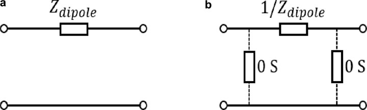
Figure 3. (a) 2-port network model for the antenna with impedance
The final result of the calibration procedure is to determine the unknown impedance of the antenna
We also write the 3-port S-parameter matrix for the balun1 network in terms of its admittance parameters as given in Equation 9a. Equations for converting S-parameters of a 3-port network to Y-parameters is given in the Supplementary Appendix. Figure 4 shows a network schematic combining the four networks, balun1, stem1a and stem1b, and the antenna. This leads to the following system of equations and constraints.
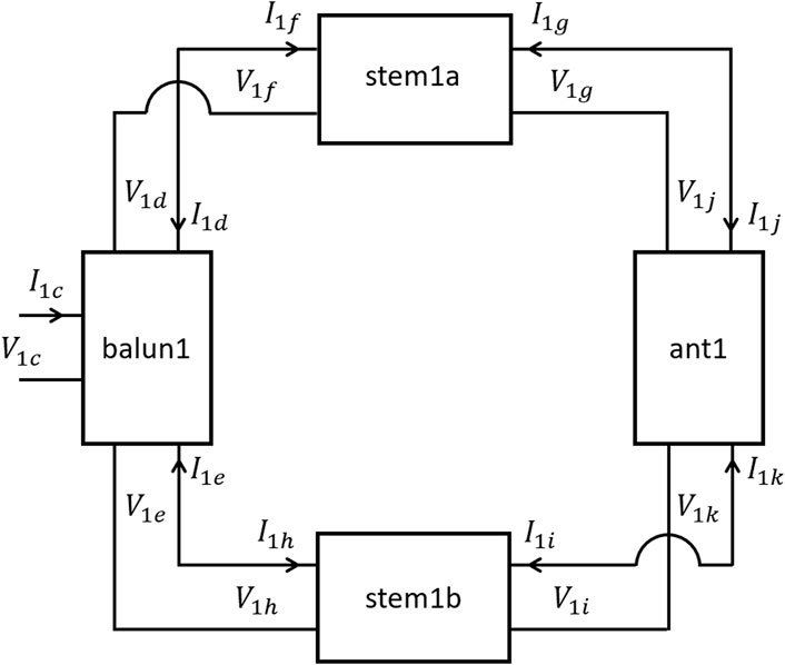
Figure 4. Network diagram model of the antenna, coaxial stems, and balun portion of the switch matrix of the on-board calibration circuit, indicating the voltage and current at each port. We use the convention of positive current flows in to each port.
We simplify the expressions, given in Equations 9a–e, by equating potentials and currents that merge to arrive at an effective 1-port network for the system. The resulting expression simplifies Equation 9a to Equation 10 given Equations 11, 12.
The left-hand-side of Equation 11 is equal to
The nonlinear expression in Equation 13 has only one unknown
4 Results
4.1 Step 4: characterize the standards
In order to characterize the on-board calibration standards and the balun1 network, we remove the SMA jumper between port1b and port1c. We attach a calibrated vector network analyzer to port1c and make
A summary of the characterization of the standards is presented in Figure 5, where the real part of the impedance is plotted on the x-axis and the imaginary part of the impedance is plotted on the y-axis for each standard parameterized by the frequency. The large symbol denotes the value of the impedance at the start frequency. This plot illustrates the range of complex impedances covered by the standards. Avoiding bunching of the standards for any given frequency will result in more accurate calibrations (Agilent Technologies, 2006). These measurements also provide reference impedances for the antenna and the test load to use for comparisons to calibrated measurements of the same. However, it is important to recognize that over this frequency range, the antenna measurement will incorporate effects from the ambient environment. Consequently, a calibrated antenna measurement might deviate from the reference if the conditions were not the same.
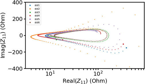
Figure 5. Plot of real and imaginary parts of the impedance for the six on-board calibration standards at each frequency. The large symbol for each set is the impedance of each standard at the start frequency. More effective calibrations are achieved by separating the standard impedances on this plane at each frequency.
4.2 Steps 8–12: characterize the balun1 network
With Port 1 of the VNA connected to port1c, the stems and antenna elements are removed at port1d and port1e. A 50 Ω terminator is connected to port1e and Port 2 of the VNA is connected to port1d. We measure the full 2-port S-parameters with the switch1h closed. This process is repeated measuring the S-parameters with the VNA connected to port1c and port1e and again with it connected to port1d and port1e, moving the 50 Ω terminator to the unused port each time. At the end of this process, we arrive at the 3-port S-parameters for the network balun1. Figure 6 shows the real and imaginary parts of the first row from the 3 × 3 S-parameter matrix, including the redundant measurement of
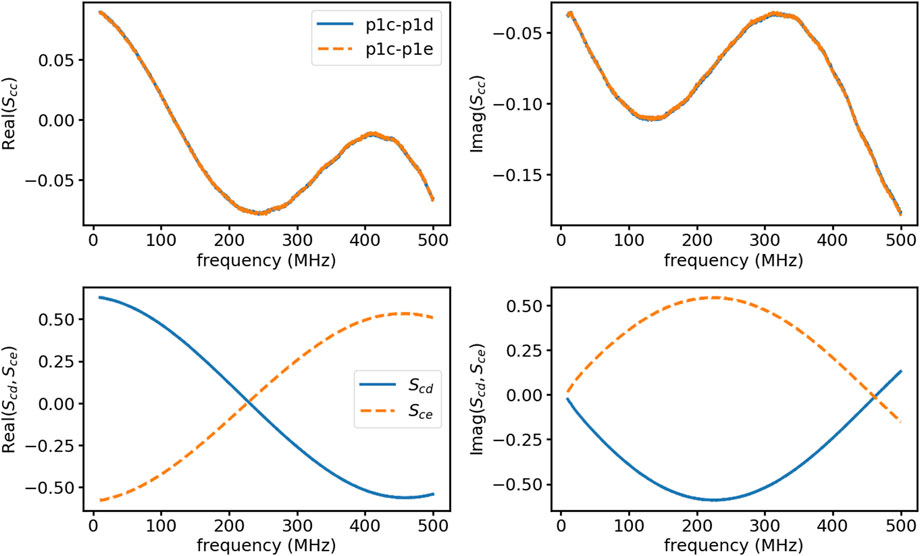
Figure 6. The first row of the network balun1 3 × 3 S-parameter matrix, including the redundant measurement of
4.3 Steps 15–18: measure standards with system and calibrate to port1c
We replace the SMA jumper between port1b and port1c and reattach the antenna and stems to port1d and port1e. We connect a function generator to port1a and rfv1 and rfi1 to an oscilloscope. We step through frequency from 10 MHz to 500 MHz and simultaneously record rfv1 and rfi1 with the RF switch in each of its eight positions. We extract the real and imaginary components of rfv1 and rfi1 by multiplying each with
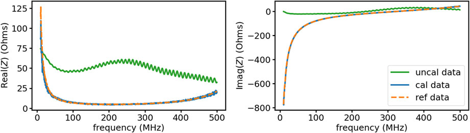
Figure 7. The real and imaginary parts of the calibrated impedance of the test load (solid blue) compared to the reference impedance (orange dashed) and uncalibrated impedance (solid green). The calibration procedure accurately recovers the test load impedance.
4.4 Step 19: iteratively solve for
Figure 8 shows a comparison of the real and imaginary parts of the impedance of the dipole antenna in vacuum determined by using the full 3-port balun and nonlinear fit to Equation 11 (solid blue). We have developed a finite element framework called the plasma complete electrode model (PCEM) (Gatling et al., 2024) for modeling our impedance probes and report the PCEM simulated dipole impedance (dashed orange). The full 3-port balun model does an excellent job of recovering the predicted free space capacitance of the dipole, which deviates from the model at high frequency, where the quasi-static approximation used in the PCEM is violated. The nonlinear fit yields a large unexpected real impedance for low frequencies; however, if we use the best fit
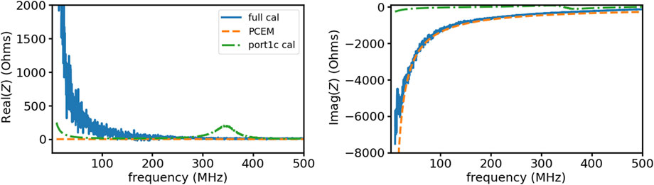
Figure 8. Real and imaginary impedance of the dipole antenna comparison using the 3-port balun model (solid blue) and the PCEM dipole model (dashed orange). Data only calibrated to port1c (red dots) has a resonance near 350 MHz and parasitic capacitance that is dominating the dipole. The calibration using the full balun model accurately recovers the expected dipole vacuum impedance calculated using our PCEM finite element simulation for a short dipole, until around 300 MHz where the curves start to deviate due to violation of the quasi-static approximation used in the PCEM.
4.5 Steps 20–21: extract plasma parameters
We generate an Argon plasma in the SPSC and make measurements of the dipole. Figure 9 shows the magnitude and phase of the fully calibrated antenna impedance in plasma (solid orange) and the same measurement only calibrated to port1c (dashed blue). The second zero crossing in the phase, indicated by the dashed gray line, where the phase transitions from inductive (
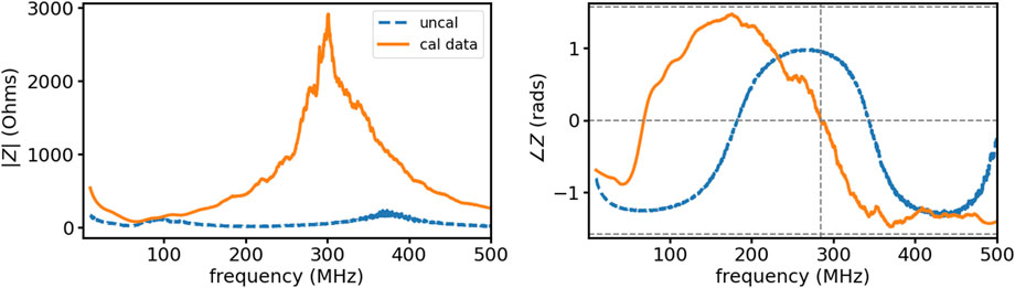
Figure 9. The magnitude and phase of the calibrated dipole impedance in a plasma. The dashed vertical gray line denotes the second zero crossing in the phase, which corresponds to the upper hybrid frequency and is used to extract the plasma density from the impedance spectrum.
For this dataset, the background magnetic field was 20 G, which yields a density
4.6 Error analysis
When initially evaluating the on-board calibration circuit, we took 100 measurements of each standard that allowed us to conduct an error analysis of the SOL calibration and to compare the effectiveness of using all six calibration standards. We use this dataset to estimate the mean and standard deviation of the underlying noise distribution. Quantile-quantile plots of our dataset are consistent with the noise being described by a bivariate normal distribution. We conduct a Monte Carlo simulation to simulate the process of calculating the calibration coefficients using the estimated noise distributions for the characterization of each standard and the measurement of each standard.
We took 100,000 samples of the noise distribution at each frequency for each measurement and constructed an ensemble of calibrations. Figure 10 shows the resulting real and imaginary parts of the standard deviation from this ensemble of the three calibration coefficients using three standards (blue) and all six standards (orange). There is a clear benefit to using all six standards to determine the calibration coefficients with the most benefit occurring for high frequencies. Figure 11 illustrates the improvement in the calibration of the test load due to using all six standards. The percent error in the calibrated test load compared to the reference as a function of frequency is plotted for the case using three standards (blue) and using all six (orange). The maximum error is reduced by 500% and the average error is reduced by 50% by using all six standards to determine the calibration coefficients.
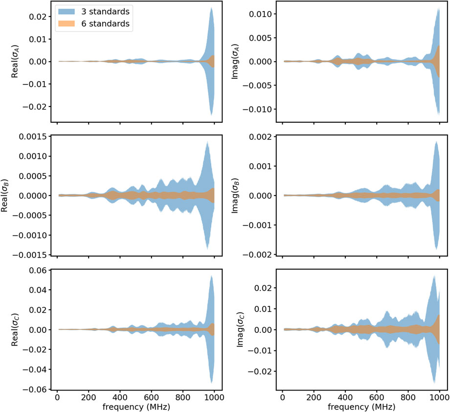
Figure 10. Comparison of the standard deviation of the three calibration coefficients from the Monte Carlo simulation using three standards (blue) and all six standards (orange). The use of all six standards reduces the variability in the determination of the calibration coefficients by over a factor of two.
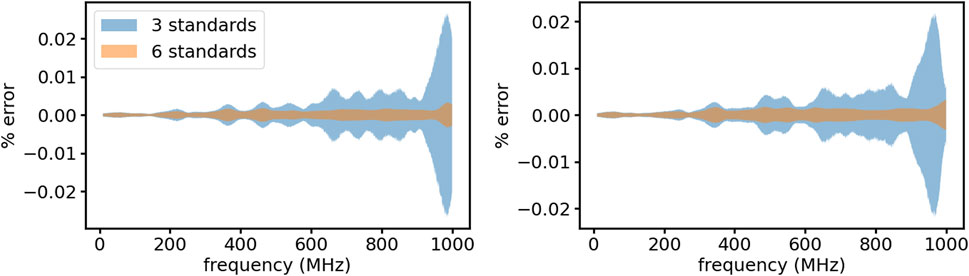
Figure 11. Percent error for the calibrated test load compared to the reference measurement as a function of frequency using the calibration coefficients derived from using three standards (blue) and all six standards (orange). The overall error in calibration of the test load is reduced using all six standards.
5 Discussion
We have presented a design for a laboratory plasma impedance probe that consists of an impedance measurement circuit, an on-board calibration circuit, and a dipole antenna. The design is suitable for measuring plasma densities up to
Data availability statement
The raw data supporting the conclusions of this article will be made available by the authors, without undue reservation.
Author contributions
ET: Conceptualization, Formal Analysis, Writing – original draft, Writing – review and editing. GG: Conceptualization, Methodology, Writing – review and editing. MP: Conceptualization, Methodology, Writing – review and editing.
Funding
The author(s) declare that financial support was received for the research and/or publication of this article. This work is supported by the US Naval Research Laboratory base program.
Conflict of interest
The authors declare that the research was conducted in the absence of any commercial or financial relationships that could be construed as a potential conflict of interest.
Generative AI statement
The author(s) declare that no Generative AI was used in the creation of this manuscript.
Publisher’s note
All claims expressed in this article are solely those of the authors and do not necessarily represent those of their affiliated organizations, or those of the publisher, the editors and the reviewers. Any product that may be evaluated in this article, or claim that may be made by its manufacturer, is not guaranteed or endorsed by the publisher.
Supplementary material
The Supplementary Material for this article can be found online at: https://www.frontiersin.org/articles/10.3389/fspas.2025.1541986/full#supplementary-material
References
Agilent Technologies (2006). “Advanced calibration techniques for vector network analyzers,” in Modern measurement techniques for testing advanced military communications and radars. 2nd Edition.
Arsenovic, A., Hillairet, J., Anderson, J., Forsten, H., Ries, V., Eller, M., et al. (2022). Scikit-rf: an open source Python package for Microwave network creation, analysis, and calibration speaker’s corner. IEEE Microw. Mag. 23, 98–105. doi:10.1109/MMM.2021.3117139
Balmain, K. (1964). The impedance of a short dipole antenna in a magnetoplasma. IEEE Trans. Antennas Propag. 12, 605–617. doi:10.1109/TAP.1964.1138278
Bauer, R. F., and Penfield, P. (1974). De-embedding and unterminating. IEEE Trans. Microw. Theory Techn 22, 282–288. doi:10.1109/TMTT.1974.1128212
Bilén, S. G., Hass, J. M., Gulczinski, F. S., Gallimore, A. D., and Letoutchaia, J. (1999). “Resonance-probe measurements of plasma densities in electric-propulsion plumes,” in AIAA 35th joint propulsion Conference and exhibit, 1999–2714. doi:10.2514/6.1999-2714
Bishop, R. H., and Baker, K. D. (1972). Electron temperature and density determination from RF impedance probe measurements in the lower ionosphere. Planet. Space Sci. 20, 997–1013. doi:10.1016/0032-0633(72)90211-5
Blackwell, D. D., Walker, D. N., and Amatucci, W. E. (2005). Measurement of absolute electron density with a plasma impedance probe. Rev. Sci. Instrum. 76, 023503. doi:10.1063/1.1847608
Bockelman, D. E., and Eisenstadt, W. R. (1995). Combined differential and common-mode scattering parameters: theory and simulation. IEEE Trans. Microw. Theory Techn. 43, 1530–1539. doi:10.1109/22.392911
Brooks, J. W., Tejero, E. M., Paliwoda, M. C., and McDonald, M. S. (2023). High-speed plasma measurements with a plasma impedance probe. Rev. Sci. Instrum. 94, 083506. doi:10.1063/5.0157625
Gatling, G., Tejero, E. M., and Wage, K. E. (2024). A complete electrode model for plasma impedance probes. Phys. Plasmas 31, 073902. doi:10.1063/5.0199553
Hopkins, M. A., and King, L. B. (2014). Assessment of plasma impedance probe for measuring electron density and collision frequency in a plasma with spatial and temporal gradients. Phys. Plasmas 21, 053501. doi:10.1063/1.4874321
Keysight Technologies Impedance measurement handbook: a guide to measurement Technology and techniques. Available online at: https://www.keysight.com/zz/en/assets/7018-06840/application-notes/5950-3000.pdf.
Kruppa, W., and Sodomsky, K. F. (1971). An explicit solution for the scattering parameters of a linear two-port measured with an imperfect test set (correspondence). IEEE Trans. Microw. Theory Techn 19, 122–123. doi:10.1109/TMTT.1971.1127466
Kurokawa, K. (1965). Power waves and the scattering matrix. IEEE Trans. Microw. Theory Techn 13, 194–202. doi:10.1109/tmtt.1965.1125964
Swenson, C. M., Fish, C., and Thompson, D. (2003). “Calibrating the floating potential measurement unit,” in Proceedings of the 8th spacecraft charging technology conference, AL. Huntsville.
Tejero, E. M., and Gatling, G. (2009). Linear decomposition method for approximating arbitrary magnetic field profiles by optimization of discrete electromagnet currents. Rev. Sci. Instrum. 80, 035104. doi:10.1063/1.3093799
Walker, D. N., Fernsler, R. F., Blackwell, D. D., and Amatucci, W. E. (2008). Determining electron temperature for small spherical probes from network analyzer measurements of complex impedance. Phys. Plasmas 15, 123506. doi:10.1063/1.3033755
Walker, D. N., Fernsler, R. F., Blackwell, D. D., and Amatucci, W. E. (2010). Using rf impedance probe measurements to determine plasma potential and the electron energy distribution. Phys. Plasmas 17, 113503. doi:10.1063/1.3501308
Keywords: plasma impedance probe, plasma diagnostic, calibration, RF impedance measurement, self impedance
Citation: Tejero EM, Gatling G and Paliwoda MC (2025) Calibration of a laboratory plasma impedance probe. Front. Astron. Space Sci. 12:1541986. doi: 10.3389/fspas.2025.1541986
Received: 09 December 2024; Accepted: 24 June 2025;
Published: 08 July 2025.
Edited by:
Julio Urbina, The Pennsylvania State University (PSU), United StatesReviewed by:
Enrique Rojas Villalba, Massachusetts Institute of Technology, United StatesSven Bilen, The Pennsylvania State University (PSU), United States
Copyright © 2025 Tejero, Gatling and Paliwoda. This is an open-access article distributed under the terms of the Creative Commons Attribution License (CC BY). The use, distribution or reproduction in other forums is permitted, provided the original author(s) and the copyright owner(s) are credited and that the original publication in this journal is cited, in accordance with accepted academic practice. No use, distribution or reproduction is permitted which does not comply with these terms.
*Correspondence: Erik M. Tejero, ZXJpay5tLnRlamVyby5jaXZAdXMubmF2eS5taWw=