 Wenjie Zhao1,2
 Jianing Rao1,2*Cheng Hao1Wenyuan Jia1Zhenxing Dong1,2Xiaoyong Ma1Miao Ma1Wenhui Yang1,2Yan Zhu1,2Junshe An1,2
- 1National Space Science Center, The Chinese Academy of Sciences, Beijing, China
- 2University of Chinese Academy of Sciences, Beijing, China
This paper focuses on the strategic importance of China’s Chang’e series of deep-space exploration missions and the urgent challenges faced in equipment development, and proposes a highly integrated and universal ground testing platform design. As the core component of China’s lunar exploration program, the successful implementation of the Chang’e series marks China’s technological breakthroughs and strategic layout in the field of deep-space exploration. With the completion of the world’s first lunar far-side sample return mission by Chang’e-6, subsequent missions have placed higher demands on equipment development. Traditional customized ground testing systems for single missions suffer from long development cycles and low rates of technology reuse. To address these issues, this paper proposes a universal ground testing device that integrates remote control and telemetry communication, scientific data transmission, as well as AD (Analog-to-Digital) and OC (Open Collector) signal detection, and DA (Digital-to-Analog) and Open Collector signal output functions through a modular architecture. This enables multi-mission compatibility and rapid deployment. The proposed ground testing device effectively shortens the development cycle of onboard equipment, achieves a high rate of technology reuse, and reduces costs, providing technical support for the efficient advancement of China’s deep-space exploration program.
1 Introduction
With the continuous advancement of China’s ambitious space program, the significance and proportion of deep space exploration, especially lunar exploration predominantly carried out through the highly successful Chang’e series of missions, have been on a consistent upward trajectory. The scientific objectives associated with these exploratory missions are in a state of perpetual evolution, growing in complexity and sophistication (Zhao et al., 2020; Xue et al., 2024). This evolution encompasses not only an expansion in the scope of exploration but also an increase in the precision and depth of scientific investigations. For instance, earlier Chang’e missions were primarily focused on basic lunar topography mapping, while more recent and upcoming missions aim to delve deeper into aspects such as lunar regolith composition analysis, in-situ resource utilization experimentation, and high-resolution remote sensing of the lunar polar regions. As a result, the requirements for scientific exploration have become increasingly diverse, demanding real-time data acquisition and transmission capabilities, as well as extremely high levels of accuracy in measurements and observations. Such enhanced requirements have substantially augmented the intricacy and difficulty involved in the development of deep space exploration equipment (IEEE/ANSI, 2014).
Ground testing equipment for space devices has emerged as a linchpin in the success of these missions. This type of equipment plays a crucial role as it is used to simulate the harsh and unforgiving space environments on Earth prior to the actual launch of satellites. The testing equipment for satellite payload electronics, in particular, is integral to the assessment and validation of the performance and functionality of various payload components that are part of the satellite. It encompasses all stages of device testing, including but not limited to component-level verification, subsystem integration testing, and system-level simulation (Wolf and Daout, 2020).This comprehensive testing framework is essential to ensure that the payload electronics can withstand the rigors of spaceflight, accurately perform their intended scientific functions, and communicate effectively with ground stations.
However, one of the major challenges in the development of such ground testing equipment lies in the inherent diversity of payload electronic devices. Due to the independent development nature of these devices, each device typically comes with its own unique electronic and hardware interfaces. This diversity means that the testing requirements for individual devices can vary significantly from one another. For example, a high-resolution imaging spectrometer may require precise wavelength calibration and high-speed data acquisition capabilities, while a lunar seismometer may need to be tested for sensitivity, noise levels, and long-term stability in extreme temperature conditions. As a result, traditional approaches to designing ground testing equipment often face limitations (ECSS, 2008).
In conventional designs, various board modules are integrated into a host computer chassis to perform the testing tasks, as typically represented in Figure 1. While this approach has its merits in terms of modularity and ease of maintenance, it also has certain drawbacks. Firstly, the capacity and capabilities of the chassis motherboard impose significant constraints on the number and types of interfaces that can be provided. This limitation makes it difficult to accommodate the diverse and complex interface requirements of multiple payload devices simultaneously. As a result, designers often find themselves having to make compromises in terms of the number of interfaces available or the flexibility of the system, which can significantly impact the overall effectiveness and usability of the ground testing equipment. Secondly, the relatively independent nature of each module in the system means that they typically require separate development efforts. This leads to increased software development costs, longer development cycles, and a lower level of design integration. Each module needs to be developed, tested, and integrated individually, which not only consumes significant resources but also makes it challenging to achieve seamless communication and coordination between different modules.
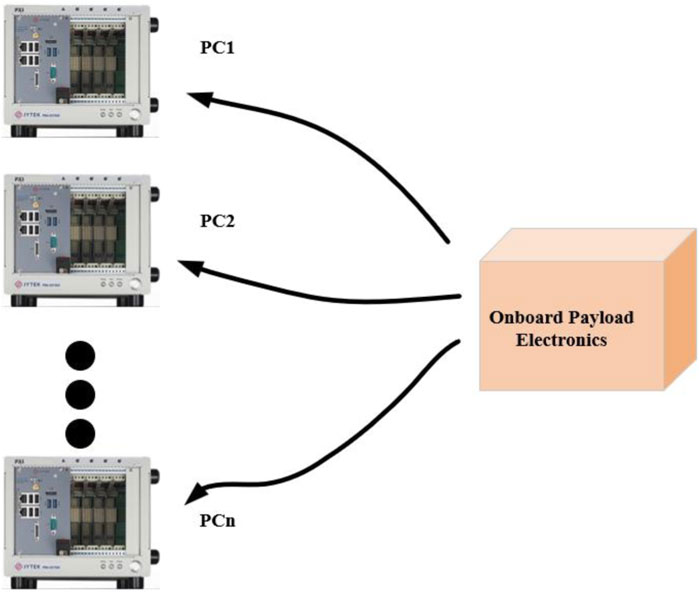
Figure 1. Traditional ground test equipment system.
In response to these challenges, this paper presents an optimized design approach that addresses the shortcomings inherent in traditional methods. Based on a thorough analysis of the existing limitations, we propose a highly integrated electronic ground testing equipment, as detailed in Figure 2. This new design offers a comprehensive and robust solution that overcomes the limitations of traditional approaches and provides enhanced capabilities for testing a wide range of payload electronics.
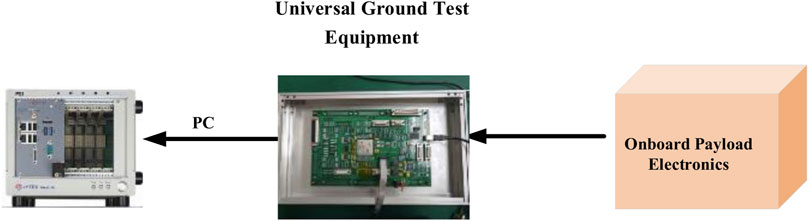
Figure 2. Universal ground test equipment system.
The designed ground testing hardware includes RS422 data interfaces, LVDS data interfaces, AD data acquisition interfaces, OC data acquisition interfaces, DA output data interfaces, OC output data interfaces, debugging interfaces, USB host communication interfaces, serial port host communication interfaces, and program data storage interfaces. These interfaces can connect with actual payload electronics and the host computer, providing sufficient data processing capabilities and a sufficient number of data interfaces, making it practically applicable to various payload electronics through different configurations.
In essence, this highly integrated electronic ground testing equipment represents a significant leap forward in testing capabilities for deep space exploration missions. By addressing the limitations of traditional designs through innovative hardware and software solutions, this new approach not only enhances the efficiency and effectiveness of testing but also paves the way for future advancements in space exploration technologies.
2 Hardware design of universal ground test equipment
2.1 Overall hardware design
The designed ground testing hardware includes RS422 data interfaces, LVDS data interfaces, 2,711 high speed data interfaces, AD data acquisition interfaces, OC data acquisition interfaces, DA output data interfaces, OC output data interfaces, debugging interfaces, USB host communication interfaces, serial port host communication interfaces, and program data storage interfaces. These interfaces can connect with actual payload electronics and the host computer, providing sufficient data processing capabilities and a sufficient number of data interfaces, making it practically applicable to various payload electronics through different configurations. The hardware design block diagram is shown in the Figure 3. The electronic design of the universal ground test equipment utilizes an SRAM-based FPGA as the main control chip to drive different interface chips for various interface data communications, and configures corresponding memory chips to store the relevant programs or data.
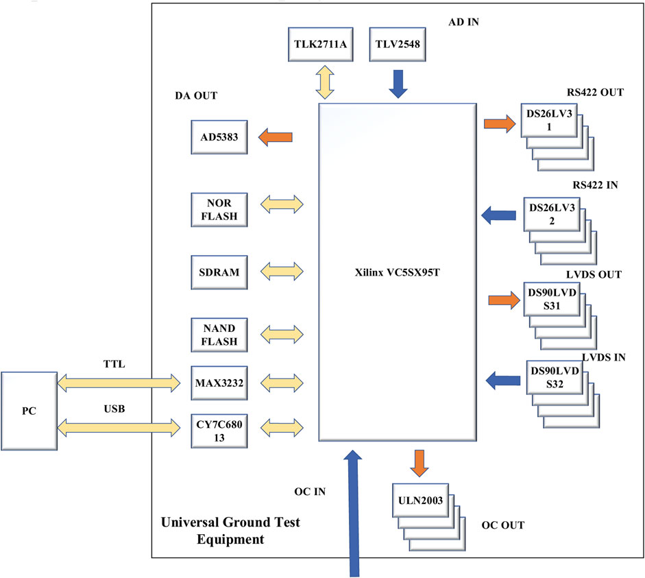
Figure 3. The hardware design block diagram.
2.2 RS422 and LVDS hardware design
RS422 and LVDS are both signal transmission technologies widely used in industrial, communication, and embedded systems, characterized by their high efficiency, stability, and strong anti-interference capabilities.
The differential voltage formula for RS422 and LVDS is:
Although the simple design knowledge we utilize in industrial applications is often sufficient, the use of RS422 and LVDS in aerospace projects demands a more rigorous analysis of their performance. Based on this analysis, a more comprehensive hardware design is required.
RS422 requires a parallel termination resistor at the receiver to suppress signal reflections:
Cable length is limited by signal attenuation and delay. Empirical formula:
Where
Common-mode rejection ratio of the differential receiver directly impacts noise immunity:
Where
So we should ensure signal bandwidth meets the rise time requirement:
As to LVDS, it requires strict differential impedance matching (typically 100Ω), determined by PCB trace parameters:
Relationship between LVDS constant-current drive (typically 3.5 mA) and power consumption:
We should ensure signal jitter does not exceed 10%–15% of the unit interval (UI):
For high-frequency designs, consider PCB propagation delay:
Radiated emissions correlate with signal slew rate. LVDS inherently suppresses EMI due to low voltage swing (350 mV):
Reduce
Therefore, we implemented a universal stability design, beginning with the establishment of a signal attenuation model. High-frequency signal attenuation in cables (unit: dB/m):
R: Resistance per unit length.
G: Conductance per unit length.
ω: Signal angular frequency.
Relationship between eye diagram opening and noise margin:
Impact of power supply noise on common-mode voltage:
PSRR: Power Supply Rejection Ratio (typically > 40 dB for LVDS).
The hardware design of RS422 and LVDS in general ground testing equipment is not entirely similar to the communication bus design in the industrial sector, primarily requiring attention to various construction standards and wide-ranging adaptability. Due to the differing hardware designs and communication protocols of various payloads, the design in this paper needs to accommodate a variety of aerospace construction standards and different protocols, which is also the main challenge of this section’s design. We achieve compatibility with various construction standards through the design of different matching resistors, confirming the construction standards before assembly and proceeding with electrical debugging, enabling the ground testing equipment to better simulate the most authentic working state of each payload’s electronics.
Figures 4, 5 illustrate the complex construction standards for RS422 and LVDS, respectively. However, not all payloads adhere to the same construction standards. Therefore, when designing this universal ground testing equipment, it is crucial to ensure compatibility with various construction standards. These standards are primarily categorized into one-to-one transmission mode, one-to-many transmission mode, and many-to-many corresponding transmission mode.
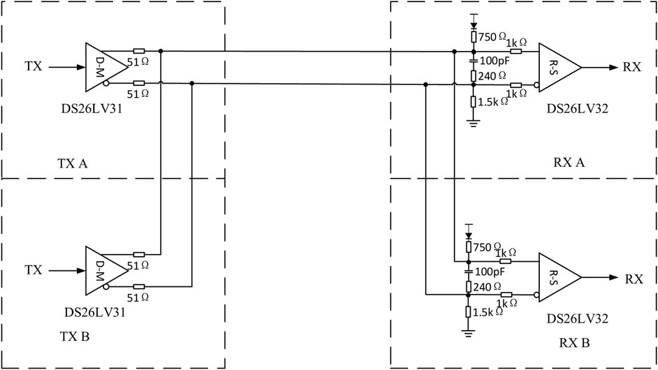
Figure 4. The complex RS422 construction standards.
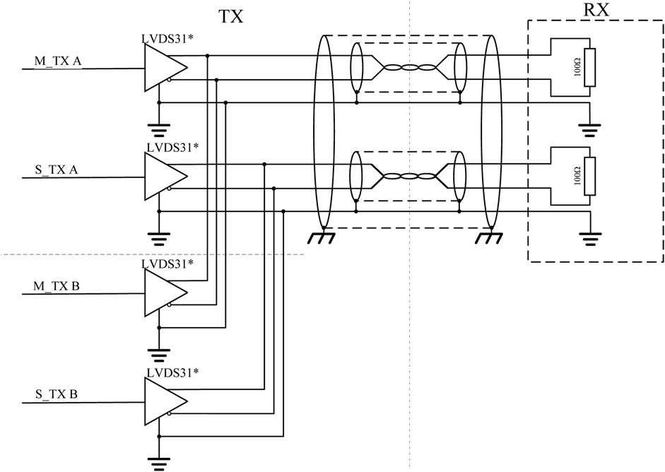
Figure 5. The complex LVDS construction standards.
2.3 2,711 hardware design
The TLK2711-SP performs parallel-to-serial and serial-to-parallel data conversion. The clock extraction functions as a physical layer (PHY) interface device. The serial transceiver interface operates at a maximum speed of 2.4 Gbps. The transmitter latches 16-bit parallel data at a rate based on the supplied reference clock (TXCLK). The 16-bit parallel data is internally encoded into 20 bits using an 8-bit/10-bit (8b/10b) encoding format. The resulting 20-bit word is then transmitted differentially at 20× the reference clock (TXCLK) rate. The receiver section performs the serial-to-parallel conversion on the input data, synchronizing the resulting 20-bit wide parallel data to the recovered clock (RXCLK). It then decodes the 20-bit wide data using the 8-bit/10-bit decoding format resulting in 16 bits of parallel data at the receive data pins (RXD0–RXD15). The outcome is an effective data payload of 1.28–2 Gbps (16 bits data × the frequency) (Zhao et al., 2022).
To evaluate the stability of the hardware design when using the 2,711 for high-speed communication, several aspects must be considered, such as signal integrity, power integrity, and electromagnetic compatibility.
In practical hardware design, it is essential to ensure that the bandwidth of components such as transmission lines, drivers, and receivers can meet the rise time requirements, typically ranging from a few picoseconds to several tens of picoseconds. Failure to do so may result in signal distortion, intersymbol interference, and other issues that could compromise the stability of communication. Eye diagrams can intuitively reflect the integrity of a signal. Subsequently, we will conduct practical verification through the use of eye diagrams.
Regarding the power integrity of the 2,711, power supply ripple can affect the operational stability of the chip. The ripple voltage
In communications above 2.0 Gbps, the chip’s switching frequency is high, necessitating sufficient decoupling capacitance to reduce power supply ripple.
In the design of aerospace hardware products, electromagnetic compatibility is a critical concern that requires significant attention. The near-field radiation intensity S of a universal ground testing equipment can be estimated using the Poynting vector. For a simple current loop, the radiation intensity is related to the loop’s area A, the current I, and the frequency f. In the far-field region, the radiated electric field strength E can be approximately expressed as:
Where k is a constant (approximately 1.38 × 10⁻²³ J/K), and r is the distance from the observation point to the loop.
To meet electromagnetic compatibility requirements, the radiated electric field strength needs to be below the relevant standard limits. In practical design, it is necessary to arrange the wiring reasonably and reduce the area of the current loop to minimize radiation intensity.
2,711 can work in full duplex mode or receive or transmit separately. In the hardware design, we need to pay more attention to its working mode and output level type.
Block of hardware circuit design in full duplex mode is shown in Figure 6.
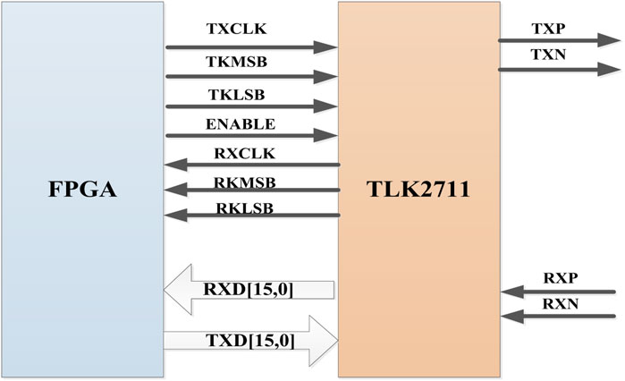
Figure 6. Block of full duplex mode.
In full duplex mode, all control bus and data bus should be connected to FPGA and the differential input and output lines should be connected to the connectors.
In this part, the most important point to note is its signal transmission mode, this is also the key to achieve the predetermined data rate in circuit design. High-speed I/O mode is shown in Figure 7.
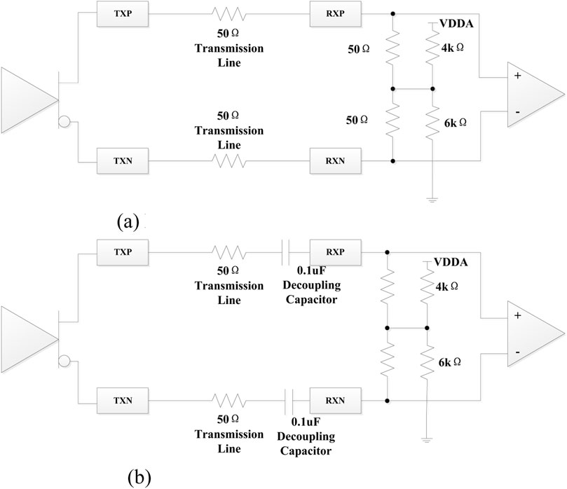
Figure 7. High-speed I/O mode. (a) High-speed I/O direct-coupled mode. (b) High-speed I/O AC-Coupled mode.
Figure 7a is high-speed I/O Direct-Coupled mode, and Figure 7b is high-speed I/O AC-Coupled mode. We usually use the high-speed I/O AC-Coupled mode. In this mode, it is important that the transmission impedance should be set to 50Ω, and the decoupling capacitors are set to 0.1uF. The decoupling capacitors can be placed at the transmitting end at the same time to avoid forgetting to place the decoupling capacitors at other receiving ends. How to control the impedance of the differential transmission line will be described in detail in the next section.
It should also be noted that the differential voltage level of TLK2711 is VML type, and the matched transceiver chip needs to be VML type to ensure normal data rate and data accuracy. Various commonly used differential level types are shown in Figure 8.
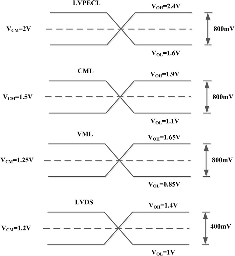
Figure 8. Graphic voltage swings by logic level.
2.4 Functional description of universal ground test equipment
The designed ground testing hardware includes RS422 data interfaces, LVDS data interfaces, AD data acquisition interfaces, OC data acquisition interfaces, DA output data interfaces, OC output data interfaces, debugging interfaces, USB host communication interfaces, serial port host communication interfaces, and program data storage interfaces. These interfaces can connect with actual payload electronics and the host computer, providing sufficient data processing capabilities and a sufficient number of data interfaces, making it practically applicable to various payload electronics through different configurations.
First, as a universal ground testing system, it must be capable of simulating various space payloads to transmit scientific data and analog telemetry. Space payloads typically send scientific data through different interfaces, including: low-speed data: RS422 bus and high-speed data: LVDS bus and 2,711 bus. Given the variations in communication bus speeds (ranging from kbps to Gbps) and differences in hardware implementation (e.g., RS422 uses differential signaling, while LVDS requires impedance matching), and considering that different space payloads have varying interface configurations (e.g., optical payloads often use LVDS, while detection payloads commonly employ 2,711), this system is equipped with multiple RS422/LVDS/2,711 bus interfaces.
This design can simultaneously emulate up to more than five (specific quantity based on configuration) space payloads, fully supporting core functionalities such as: scientific data downlink, analog telemetry acquisition, remote command interaction.
For instance, in a previous standalone unit project, our designed Payload Management Unit (PMU) required the ground test system to simulate space payloads with the functions of RS422 bidirectional telemetry/command communication, LVDS and 2,711 scientific data transmission, AD telemetry acquisition, OC command control. In this project, the universal ground test equipment successfully emulated five different payloads simultaneously with the following interface configurations (Figure 9).
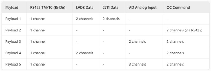
Figure 9. Payload configuration simulated by UGT
The test setup between the universal ground test equipment and the PMU is shown in Figure 10.
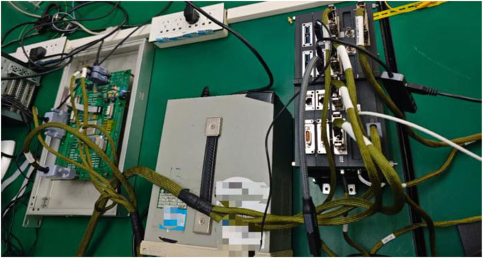
Figure 10. The UGT with payload management unit (PMU).
Due to the development of different aerospace equipment by different units, it is often difficult to have a common time for synchronous debugging during debugging. Therefore, universal ground test equipment is extremely important in debugging by simulating data interaction between different loads. By using universal ground inspection equipment, each single machine can be independently debugged for its functions. According to the interface protocol between different load devices, different modules of the UGT can be configured to simulate the receiving and transmitting functions of the load according to the protocol, greatly reducing the development time of the equipment, reducing the possibility of problems occurring during the docking between devices, and improving the reliability of equipment development.
3 Software design of universal ground test equipment
In the previous section, We have proposed a universal ground test equipment hardware design for the payload electronics of the Chang’e series spacecraft. This design is compatible with most general interfaces, different construction standards, and communication protocols, and it provides an ample number of interfaces. Theoretical calculations have shown that its reliability is sufficiently guaranteed. This section primarily focuses on the software design of the universal ground test equipment (ISO, 2002; Nguyen and Miller, 2012; Bitman, 2011).
3.1 Overall software design
The main idea is to implement a configurable modular software design, which can significantly reduce the workload of software designers and enhance the broad applicability of the universal ground test equipment, even when applied to different projects. The architecture of the overall software is illustrated in the Figure 11.
Figure 11. The architecture of the overall software.
3.2 Modular software design
As shown in Figure 11, We have categorized the primary functions of the ground test equipment into 11 functional modules: RS422 transmission, RS422 reception, LVDS transmission, LVDS reception, DA output, AD acquisition, 2,711 transceiver, OC output, OC input, TTL debugging, and USB debugging. Depending on the practical application scenarios of each module, various protocols can be configured within the modules through software, offering strong adaptability in the number of interfaces and simplifying the debugging process (He et al., 2020).
By connecting to the upper computer through the FPGA serial port, UGT module configuration parameters can be controlled through both FPGA software and upper computer software, such as RS422 transmission code rate and frame format, LVDS transmission rate and frame format, 2,711 transmission rate and frame format, DA output analog quantity size and OC control time, etc.
3.3 Host computer software design
We connect the universal ground test equipment to the host computer via USB, with the host computer primarily handling data interaction, recording, and control of the universal ground test equipment. By designing the host computer’s universal ground test control software using QT, we can control the transmission of various types of data from the universal ground test equipment, collect the valid data received by the equipment, and save, analyze, and process the data. This control software also allows for adjustable DA output to verify the AD acquisition capabilities of the actual equipment. This setup realizes a complete spacecraft equipment debugging and testing system as illustrated in Figure 2. Such a comprehensive testing system has been applied in the development of multiple aerospace products, demonstrating high reliability and ease of development.
4 Experiment of universal ground test equipment
The universal ground testing equipment we have designed has been in operation for over 5 years and has been utilized in the testing of electronics for more than 20 Chang’e series and other series of aerospace equipment, with the longest single test duration exceeding 500 h. Due to the meticulousness of our software and hardware design, our universal ground testing equipment has never encountered any issues during the testing process. It has excellently completed various testing tasks simulating the space environment, thereby saving a significant amount of precious time for aerospace missions.
The actual test output waveform of RS422 is shown in Figure 12a. The actual test output waveform of LVDS is shown in Figure 12b. The actual test output waveform of OC is shown in Figure 12c. Test equipment is Tektronix MSO 4104B.
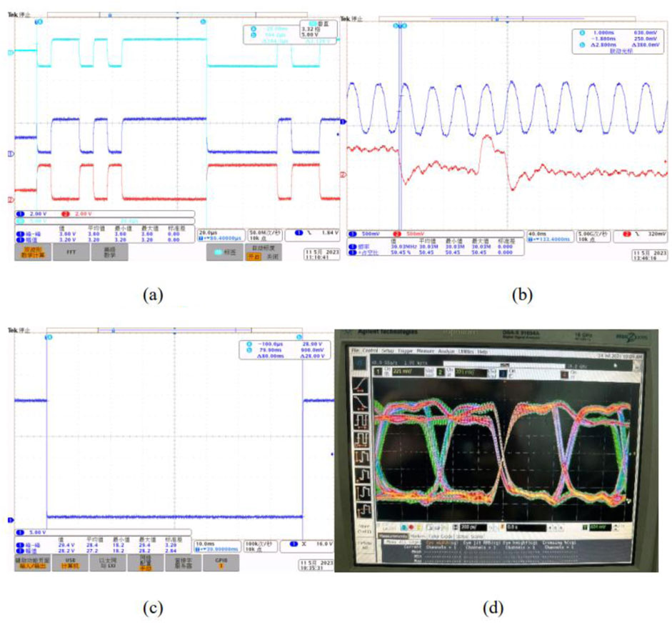
Figure 12. Actual test output waveform of (a) RS422 (b) LVDS (c) OC and (d) 2,711.
The actual test output eye diagram of 2,711 is shown in Figure 12d. Test equipment is Agilent Technologies DSA-X 91604A.
The waveform analysis demonstrates that: the RS422 interface’s baud rate is adjustable up to 115.2 kbps through UGT configuration; LVDS three-wire waveforms show excellent signal correspondence and synchronization; OC output maintains highly stable pulse width timing (measured variation <0.5%); the 2,711 eye diagram generated by UGT exhibits: Horizontal opening >85% of unit interval, Vertical margin exceeding 70% of amplitude range, Jitter <5% UI p-p.
Which RS422 timing complies with ANSI/TIA/EIA-422-B, LVDS characteristics meet IEEE 1596.3 Class II, OC timing satisfies ECSS-E-ST-50-12C, 2,711 performance exceeds CCSDS 131.0-B-3 requirements.
UGT has accompanied formal aerospace equipment in temperature cycling tests, thermal vacuum tests, mechanical tests, EMC tests, aging tests, etc. It has maintained a stable working state and completed each test with zero errors after multiple long-term power on tests. The test specifications are carried out according to the requirements of the satellite test outline, and the test environment is relatively harsh. Many of the official space equipment that UGT has tested are currently operating in orbit and in good working condition. Figure 13 is the picture of thermal vacuum test of UGT and formal aerospace equipment. The test conditions are shown in Table 1.
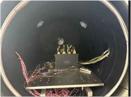
Figure 13. Thermal vacuum test of UGT and formal aerospace equipment.
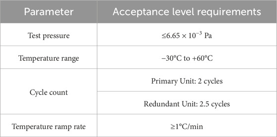
Table 1. Conditions of thermal vacuum test.
5 Conclusion
The UGT equipment we have designed has been in operation for over 5 years and has been utilized in the testing of electronics for more than 20 Chang’e series and other series of aerospace equipment, with the longest single test duration exceeding 500 h. Due to the meticulousness of our software and hardware design, our universal ground testing equipment has never encountered any issues during the testing process.
Having undergone multiple rounds of various aerospace-grade tests, this universal ground test design has demonstrated high reliability, ease of development, broad versatility, and strong applicability. It has provided robust testing technical support for the Chang’e series spacecraft and other critical aerospace products, significantly shortening the development cycle of aerospace products and reducing development costs.
Internationally, UGT is usually configured using NI chassis, but NI chassis has limited capacity and cannot simulate multiple loads working simultaneously. Unless a large number of NI chassis are configured and developed separately, it not only increases equipment costs but also software development costs, which is actually not friendly to aerospace equipment development. The UGT we designed has effectively solved this problem, reducing the development costs of software and hardware while improving efficiency.
At the same time, our UGT also has some issues, such as in the near future, aerospace equipment will have communication buses with higher speed processes, such as fiber optic communication, laser communication, etc. Our UGT does not yet have the ability to simulate these interfaces. In the future use and improvement, we will gradually add and strictly test these functions, and seriously solve these unresolved problems.
In essence, this highly integrated electronicUHTequipment represents a significant leap forward in testing capabilities for deep space exploration missions. By addressing the limitations of traditional designs through innovative hardware and software solutions, this new approach not only enhances the efficiency and effectiveness of testing but also paves the way for future advancements in space exploration technologies.
Data availability statement
The original contributions presented in the study are included in the article/supplementary material, further inquiries can be directed to the corresponding author.
Author contributions
WZ: Writing – original draft, Conceptualization, Writing – review and editing. JR: Data curation, Software, Writing – original draft. CH: Writing – review and editing, Conceptualization. WJ: Writing – review and editing, Resources, Project administration. ZD: Writing – review and editing, Validation. XM: Writing – review and editing, Investigation. MM: Writing – review and editing. WY: Writing – review and editing, Validation. YZ: Writing – review and editing, Project administration. JA: Methodology, Writing – review and editing, Validation, Resources, Visualization, Project administration.
Funding
The author(s) declare that no financial support was received for the research and/or publication of this article.
Conflict of interest
The authors declare that the research was conducted in the absence of any commercial or financial relationships that could be construed as a potential conflict of interest.
Generative AI statement
The author(s) declare that no Generative AI was used in the creation of this manuscript.
Publisher’s note
All claims expressed in this article are solely those of the authors and do not necessarily represent those of their affiliated organizations, or those of the publisher, the editors and the reviewers. Any product that may be evaluated in this article, or claim that may be made by its manufacturer, is not guaranteed or endorsed by the publisher.
References
Bitman, J. (2011). “An in-depth look at the radio frequency ground support equipment for the radiation belt storm probes mission,” in 2011 IEEE AUTOTESTCON. Baltimore, MD, 182–188. doi:10.1109/AUTEST.2011.6058725
ECSS (2008). Space Engineering - electromagnetic compatibility. European Corporation for Space Standardization.
He, Z., Wang, D., Wei, J., Zhu, H., and Wang, J. (2020). “Fast intermittent fault detection algorithms in static test of multiple ground stations,” in 2020 Chinese automation congress (CAC). Shanghai, China, 4468–4473. doi:10.1109/CAC51589.2020.9327271
IEEE/ANSI(2014). “American national standard for methods of measurement of radio - noise emissions from low-voltage electrical and electronic equipment in the range of 9 kHz to 40 GHz,” in ANSI PC63.4, May 2014 (Revision of ANSI C63.4-2009), 1–152.
Nguyen, H. D., and Miller, I. A. (2012). Cost impact of automated acceptance testing of electrical ground support equipment for spacecraft testing. IEEE Instrum. and Meas. Mag. 15 (4), 28–33. doi:10.1109/MIM.2012.6263981
Wolf, K. F. J., and Daout, B. (2020). Alternative test set-up for testing the immunity of spacecraft equipment against discharge of electrostatic energy (ESD). IEEE Electromagn. Compat. Mag. 9 (1), 69–76. doi:10.1109/MEMC.2020.9075039
Xue, X., Zhang, Y., and Zheng, W. (2024). “Design of satellite-ground integrated universal test scheme for spacecraft navigation receivers,” in 2024 3rd international symposium on sensor technology and control (ISSTC) (China: Zhuhai), 160–166. doi:10.1109/ISSTC63573.2024.10824060
Zhao, W., et al. (2022). “A novel space high speed data transmission system of 2.4Gbps,” in 2022 IEEE 5th International Conference on Electronics Technology (ICET). Chengdu, China, 1055–1059. doi:10.1109/ICET55676.2022.9824727
Zhao, Y., Zhang, T., Wu, X., and Zhang, H. (2020). “Control strategy of lunar lander-relay satellite antenna acquisition and tracking for Chang’e-4 lunar exploration mission,” in 2020 15th IEEE Conference on Industrial Electronics and Applications (ICIEA), Kristiansand, Norway, 1506–1510. doi:10.1109/ICIEA48937.2020.9248324
Keywords: Chang’e project, deep space exploration, ground testing system, modular design, technology reuse
Citation: Zhao W, Rao J, Hao C, Jia W, Dong Z, Ma X, Ma M, Yang W, Zhu Y and An J (2025) A universal ground test equipment design for the Chang’e series spacecraft. Front. Astron. Space Sci. 12:1594802. doi: 10.3389/fspas.2025.1594802
Received: 17 March 2025; Accepted: 30 June 2025;
Published: 14 July 2025.
Edited by:
Massimiliano Galeazzi, University of Miami, United StatesReviewed by:
Anshu Kumari, NASA Goddard Space Flight Center, United StatesNicholas Thomas, National Aeronautics and Space Administration, United States
Copyright © 2025 Zhao, Rao, Hao, Jia, Dong, Ma, Ma, Yang, Zhu and An. This is an open-access article distributed under the terms of the Creative Commons Attribution License (CC BY). The use, distribution or reproduction in other forums is permitted, provided the original author(s) and the copyright owner(s) are credited and that the original publication in this journal is cited, in accordance with accepted academic practice. No use, distribution or reproduction is permitted which does not comply with these terms.
*Correspondence: Jianing Rao, cmFvamlhbmluZ0Buc3NjLmFjLmNu