 Imran Ali1
 Sasi Kumar Tippabhotla1
 Ihor Radchenko1
 Ahmed Al-Obeidi2Camelia V. Stan3Nobumichi Tamura3
 Arief Suriadi Budiman1*
- 1Xtreme Materials Laboratory (XML), Engineering Product Development (EPD) Pillar, Singapore University of Technology and Design (SUTD), Singapore, Singapore
- 2Massachusetts Institute of Technology (MIT), Cambridge, MA, United States
- 3Advanced Light Source, Lawrence Berkeley National Laboratory (LBNL), Berkeley, CA, United States
Silicon is considered as a promising anode material for the next-generation lithium-ion battery (LIB) due to its high capacity at nanoscale. However, silicon expands up to 300% during lithiation, which induces high stresses and leads to fractures. To design silicon nanostructures that could minimize fracture, it is important to understand and characterize stress states in the silicon nanostructures during lithiation. Synchrotron X-ray microdiffraction has proven to be effective in revealing insights of mechanical stress and other mechanics considerations in small-scale crystalline structures used in many important technological applications, such as microelectronics, nanotechnology, and energy systems. In the present study, an in situ synchrotron X-ray microdiffraction experiment was conducted to elucidate the mechanical stress states during the first electrochemical cycle of lithiation in single-crystalline silicon nanowires (SiNWs) in an LIB test cell. Morphological changes in the SiNWs at different levels of lithiation were also studied using scanning electron microscope (SEM). It was found from SEM observation that lithiation commenced predominantly at the top surface of SiNWs followed by further progression toward the bottom of the SiNWs gradually. The hydrostatic stress of the crystalline core of the SiNWs at different levels of electrochemical lithiation was determined using the in situ synchrotron X-ray microdiffraction technique. We found that the crystalline core of the SiNWs became highly compressive (up to -325.5 MPa) once lithiation started. This finding helps unravel insights about mechanical stress states in the SiNWs during the electrochemical lithiation, which could potentially pave the path toward the fracture-free design of silicon nanostructure anode materials in the next-generation LIB.
Introduction
In today’s modern world, efficient energy storage systems are very important particularly for portable electronic devices, electric vehicles, solar farms, and grid stations. Among electrical storage systems, the lithium-ion battery (LIB) is the most promising candidate because of its high-energy efficiency (Omar et al., 2012), high-energy density (Lukic et al., 2008; Omar et al., 2012), high normal voltage, limited self-discharge, and no memory effect (Saw et al., 2016). It has a longer life cycle (Lukic et al., 2008) with a capacity of accepting high charging and discharging rates (Saw et al., 2016). These specifications/factors are important for battery requirement in the present modern era.
Silicon is considered as a promising anode material for next-generation LIBs because of its high theoretical charge capacity (~4,200 mAh g−1), which is roughly 10 times higher than commercially available graphite anodes (~372 mAh g−1) (Chan et al., 2008; Li et al., 2017). It has a low discharge potential (Chan et al., 2008) and attractive operating voltage (Chan et al., 2008; Li et al., 2017). Despite these benefits, silicon is not yet commercialized as an anode material in LIBs because of its large expansion up to 300% upon lithiation (Lee et al., 2001). Such large-volume changes in silicon could induce high stresses in the anode resulting in structure pulverization, cracking, delamination, and loss of electronic contact (Beaulieu et al., 2001; Li et al., 2017).
It has been found that nanoscale electrode materials can facilitate strain relaxation, shorten lithium-ion and electron diffusion paths, and increase the surface area for lithium electrode reaction (Bruce et al., 2008; Park et al., 2009). The experimental studies on the size effect have demonstrated that nanomaterials exhibit better capacity retention as compared to their bulk counterparts (Ryu et al., 2011; Lee et al., 2012; Liu et al., 2012a). Many different nanostructures have been developed, such as nanoparticles (Liu et al., 2012a; Zhou et al., 2012; Shelke et al., 2017), nanospheres (Ma et al., 2007, 2017), nanowires (Chan et al., 2008; Kennedy et al., 2016), nanotubes (Shim et al., 2016; Park et al., 2009), and nanocones (Zhang et al., 2010), with an improved cycling life and better performance.
Silicon nanowires (SiNWs) are among the nanostructures that have been studied and used as an anode material for LIBs (Liu et al., 2011; Yang et al., 2012; Kennedy et al., 2016). In these studies, the SiNWs were produced using the metal-assisted chemical etching (MACE) process resulting in an ordered and densely packed arrays of nanowires with a high aspect ratio and a uniform crystallographic out-of-plane orientation of <100> (Chang et al., 2009). This process has several advantages such as the ease of fabrications, the potential ease of scalability for the high-volume manufacturing, and low cost (Peng et al., 2007; Chang et al., 2009). Besides the ease of fabrication, SiNWs have also been widely studied because their geometry (together with nanospheres) allows simple (1D or 2D) kinetics modeling leading to the core–shell model proposed by Zhao et al. in nanospheres (Zhao et al., 2012) and Yang et al. in SiNWs (Yang et al., 2014).
Lithium reacts with crystalline SiNWs and forms core–shell structures. The core of SiNWs is found to be crystalline and the shell is amorphous lithiated silicon (LixSi) (Liu et al., 2012b). Morphology and volume change in silicon anode materials have been widely studied during/after lithiation utilizing simulation and experiments (Lee et al., 2011; Wu et al., 2012; Zhao et al., 2012). It is suggested that SiNWs have an anisotropic volume expansion with respect to axial orientation (Lee et al., 2011; Liu et al., 2011; Yang et al., 2014). Liu et al. fabricated an electrochemical cell based on SiNWs and observed morphological change in SiNWs during lithiation using in situ transmission electron microscope (TEM) (Liu et al., 2012b). Further experimental work is required to examine the morphological change in SiNWs during real battery operation.
In addition, to design and utilize high-capacity silicon nanostructures anode that could minimize fracture, it is also important to study and characterize stress states during lithiation. The stress states have been recently simulated in silicon nanostructures during lithiation (Liu et al., 2011; Zhao et al., 2012; Yang et al., 2014). Zhao et al. developed an analytical model which undergoes volume expansion and plastic deformation that described stress states in spherical crystalline silicon nanoparticle during lithiation (Zhao et al., 2012). Yang et al. (2014) reported anisotropic electromechanical model for stress generation in SiNWs upon lithiation. The most important stress developed in the lithiated outer shell of SiNWs was found to be hoop stress, which was tensile upon lithiation. However, stress at the core of SiNWs was found to be compressive (Yang et al., 2014). The model was developed by utilizing several key features observed in previous TEM studies (Liu et al., 2011, 2012b; Yang et al., 2012). The lithiation-induced stress in the silicon nanoparticles has been measured using micro-Raman spectroscopy (Zeng et al., 2016). However, up until this point, no experimental study has been reported for the direct quantitative measurements of stress states in SiNWs during electrochemical lithiation (in situ) inside a realistic battery cell (i.e., battery cells that are typically used in commercial products).
Synchrotron X-ray microdiffraction (μSXRD) has proven to be effective for revealing insights of mechanical stress and other mechanics considerations in small-scale crystalline structures in many important technological applications, such as microelectronics (Budiman et al., 2006, 2009, 2010, 2012a; Kim et al., 2012a), nanotechnology (Budiman et al., 2012b,c; Kim et al., 2012b), and photovoltaics (Rengarajan et al., 2016; Handara et al., 2017; Tippabhotla et al., 2017a). This is especially true where the knowledge of how the stress evolves during the operation of the device could reveal the effective methodology to design higher-performance, more robust, and reliable nanostructure-based systems. In the present study, this technique is used to investigate the stress states in one form of Si nanostructures, i.e., SiNWs, while they are undergoing electrochemical lithiation inside a realistic battery cell that we designed specifically to allow electrochemical lithiation of SiNWs while allowing high-energy X-ray beams to access them.
For the first time in this experimental work, direct and quantitative stress state measurements were demonstrated in SiNWs during lithiation using in situ μSXRD. This proposed methodology and the experimental procedure can also be useful to study in situ stress states in other crystalline anode materials which are undergoing a large-volume expansion during electrochemical lithiation.
Experimental Setup and Procedure
In this experimental work, the hydrostatic stress of the crystalline SiNWs is determined during lithiation (at different levels of lithiation) using the in situ μSXRD experiment. A special battery cell is designed to allow high-energy X-ray beams to access SiNWs during electrochemical lithiation inside a realistic battery cell. The morphological change in SiNWs is also examined at different levels of lithiation using scanning electron microscope (SEM). In addition, stress states and morphological change are compared. The following subsections describe the materials, the battery test cell, and the methodology of μSXRD to reveal stress states in SiNWs during lithiation.
Materials and Battery Test Cell
The SiNWs are fabricated on the surface of a p-type < 100 > silicon wafer of thickness 500 µm using MACE process at the Laboratory of Materials for Micro and Nano Systems, Massachusetts Institute of Technology (MIT). The p-type < 100 > silicon wafers used in the present study have a dopant concentration of ~5–10 × 1014/cm3 and with a resistivity of 1–25 Ω cm. Details regarding the MACE process are described elsewhere (Peng et al., 2007; Choi et al., 2008; Chang et al., 2009), and the SiNWs thus obtained were roughly 6–8 µm high, standing on a 490-µm silicon substrate as shown in the schematic diagram in Figure 1A. A 200-nm thick copper layer was later deposited on the backside of the silicon wafer for electric contact (Tippabhotla et al., 2017a). Further details about the fresh samples are available in Figure S1 in Supplementary Material.
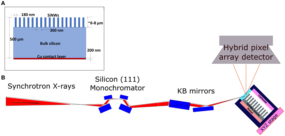
Figure 1. (A) A schematic illustration of the single-crystalline silicon nanowires (SiNWs) sample. (B) A schematic illustration of the synchrotron X-ray microdiffraction experimental setup (Kunz et al., 2009; Tippabhotla et al., 2017b).
A unique battery test cell was specially designed to enable the in situ study using μSXRD. A schematic of the test cell is shown in Figure 1B as part of the overall in situ μSXRD experiment. This unique battery test cell design is needed to allow the X-ray beam to access the SiNWs during the lithiation process inside the battery test cell, thus enabling the in situ μSXRD experiment. The design and fabrication of the battery test cell has been described in detail in our earlier report (Tippabhotla et al., 2017b). The electrochemical cycling of the test cell from open circuit voltage (OCV) of ~3–0.01 V was done on a single-channel portable Potentiostat/Galvanostat (Bio-Logic Science Instruments).
Synchrotron X-Ray Microdiffraction Experiment and Stress States in SiNWs
The μSXRD technique allows focused X-ray beam at a submicron resolution which is crucial to enable us to study stress states in SiNWs during electrochemical lithiation. The current experimental work was conducted using the μSXRD setup at beamline 12.3.2 of Advanced Light Source, Lawrence Berkeley National Laboratory, Berkeley, CA, USA (Kunz et al., 2009). The μSXRD at this beamline provides 1-µm spatial resolution and a high-crystal orientation resolution of 0.01° (MacDowell et al., 2001; Chen et al., 2016). The μSXRD technique at this beamline has been widely used to study microstructural changes and stress states in many technologically important devices and structures, such as the through-silicon via (TSV) in the microelectronics, as well as Cu/Nb nanopillars for nanotechnologies in energy applications (Budiman et al., 2006, 2012a, 2015).
Figure 1B shows the schematic diagram of the μSXRD setup. The beamline end station (BL 12.3.2) produced a high-energy (5–24 keV) polychromatic X-ray beam of 1 µm diameter. A four-crystal monochromator in the setup is used to select a single wavelength from the polychromatic beam, if required. Kirkpatrick-Baez mirrors are used as focusing optics (Kunz et al., 2009). The battery test cell was assembled on the sample stage as shown in the schematic in Figure 1B. The sample stage can move in XYZ directions where Y is along SiNWs and Z is across the SiNWs as shown and X is perpendicular to the viewing plane. The sample stage was approximately adjusted to the focus of the X-ray beam on to the SiNWs electrode using a laser triangulation system available in the beamline setup.
The SiNWs sample produced multiple diffraction signals upon interaction with the polychromatic X-ray beam. The diffracted signal was captured by a 2D X-ray hybrid pixel array (DECTRIS Pilatus 1 M) detector. Initial μSXRD scans were performed along the SiNWs (Y-direction) covering the entire thickness of the SiNWs electrode, i.e., a line scan covering SiNWs on the top and bulk Si substrate on the bottom. The resulting intensity variation of the diffracted signal along Y-direction was studied to locate the SiNWs. This is because the bulk Si generates a high-intensity diffraction signal, and the SiNWs at the same time generate a weak diffraction signal, at least 10 times lower in intensity than that of bulk Si.
Once the location of SiNWs was identified, they were scanned by both monochromatic and polychromatic X-rays before and after assembly of the battery cell. Furthermore, an in situ μSXRD scanning of the SiNWs was conducted during the electrochemical cycling of the test cell from OCV of ~3–0.01 V. Based on analysis of the initial polychromatic μSXRD scan from the SiNWs, the diffraction peaks from the crystal planes (7, 5, 1) and (6, 4, 2) with approximate energies of 14.08 and 14.62 keV, respectively, were identified for further analysis using energy scan. The first monochromatic scan was performed within the energy range of 14.02–14.14 keV with a step size of 0.002 keV for the (7, 5, 1) crystal plane. Similarly, the second monochromatic scan was performed from 14.56 to 14.7 keV with a step size of 0.002 keV for the (6, 4, 2) crystal plane. The diffraction data were analyzed using the XMAS software (Radchenko et al., 2016). From the monochromatic data analysis, we obtained the d-spacing of the diffraction planes, at different levels of lithiation (dLith). The strain (ε) in the crystalline part of the lithiated SiNWs was calculated using Eq. 1 given below (Tamura, 2014). The dUnst is the d-spacing of the respective (h,k,l) planes in the theoretically unstrained state, which in this experiment has been confirmed to be the same as that of the silicon substrate in the sample. Since the focused monochromatic X-ray beam is an ellipsoid of a few microns in size, it covers many SiNWs in this experiment, and hence the strain calculated by Eq. 1 would be an average strain over several SiNWs
Morphological Evolution of SiNWs During Electrochemical Lithiation
In addition to the μSXRD experiment, which provides stress states during the electrochemical lithiation of the SiNWs, a morphological investigation of the electrochemically lithiated SiNWs was also performed using SEM. It assessed morphological changes at different levels of lithiation, i.e., identical SiNW samples were cycled from the initial OCV (~3 V) to different final voltages (1, 0.5, and 0.01 V) using the same battery test cell used for μSXRD, and the resulting lithiated SiNWs were observed under the SEM. Before performing SEM, the lithiated SiNW samples were washed and soaked in 1:1 EC/DMC (ethylene carbonate/dimethyl carbonates) solvent and acetonitrile to remove the electrolyte salt (LiPF6) deposits to improve clarity of the SEM images. The results of this investigation show core–shell structure as commonly reported (Zhao et al., 2012; Yang et al., 2014) and help correlate with the μSXRD results.
Results and Discussion
The morphology of the lithiated SiNWs at different levels of lithiation demonstrates that the lithiation of the SiNWs is not uniform. As shown in the schematic in Figure 2A, the top surface and upper side walls of the SiNWs would get lithiated much more compared to the lower (i.e., bottom) side walls of the SiNWs. This was first illustrated in the model reported by Yang et al. (2014). Due to the lithium-ion insertion, the upper end of the SiNW expands more compared to the bottom, leaving a conical crystalline core surrounded by amorphous LixSi as shown in the schematic in Figure 2B (Yang et al., 2014). The actual SEM images shown in Figures 2C–F are in line with these schematics and confirm simulation results of morphological study (Yang et al., 2014).
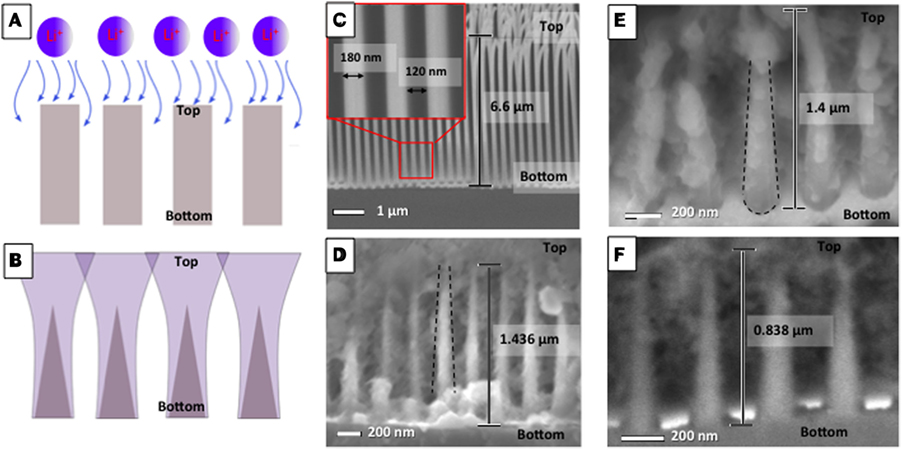
Figure 2. (Color online) (A) The schematic illustration of single-crystalline silicon nanowires (SiNWs) with insertion of lithium ions during the electrochemical lithiation. (B) The schematic diagram of SiNWs after lithiation which show that they expand anisotropically and form core–shell structure with two phases—crystalline phase of silicon (shown with dark gray color) and lithiated silicon (amorphous phase of silicon shown with light gray color). (C) Scanning electron microscope (SEM) image of pristine SiNWs, which was taken at a tilt angle of 45o. After tilt correction, the average height of SiNWs was found to be ~6.604 μm. The inset shows that the diameter and the space between SiNWs are ~180 and ~120 nm, respectively. (D) SEM image of SiNWs that have gone through lithiation from ~3 to 1 V. The average height of the cone-shaped phase of the SiNWs (which indicates the crystalline core of the lithiated SiNWs) was found to be ~1.436 μm (after tilt correction). (E) SEM image of SiNWs that have gone through lithiation from ~3 to 0.5 V. After tilt correction, the average height of the cone-shaped phase of the SiNWs was found to be ~1.402 μm. (F) SEM image of SiNWs lithiated from ~3 to 0.01 V. After tilt correction, the average height of the cone-shaped phase of the SiNWs was found to be ~0.838 μm.
The pristine SiNWs are uniform with a diameter of 180 nm and a spacing of 120 nm from each other, and a height of ~6.5 μm. Their SEM images are shown in Figure 2C. As the lithiation starts, they turn into conical structures with a sharp tip and a wide base. Figures 2D–F show SEM images of lithiated SiNWs at different levels of lithiation. The SiNWs cycled from 3 to 1 V are shown in Figure 2D. The conical, crystalline part of the SiNWs of height ~1.5 μm was observed. However, as the lithiated silicon forms LixSi, all SiNWs fused together due to expansion greater than the spacing between the SiNWs. Figures 2E,F show SEM images of the samples lithiated from ~3 V that have gone through further lithiation to 0.5 and 0.01 V, respectively. The conical, crystalline core is still visible but further reduced in heights to ~1.4 and ~0.8 μm, respectively, indicating further lithiation which progresses along the longitudinal axis of the SiNWs (from top to bottom of the SiNWs). These results are in general agreement with the widely reported core–shell lithiation model (Zhao et al., 2012; Yang et al., 2014). Further details about the lithiated samples are available in Figures S2 and S3 in Supplementary Material.
To better understand the stress states, SiNWs were initially scanned by polychromatic μSXRD (white beam), then scanned by monochromatic energy before and after the assembly of the battery cell. Before the assembly of the battery cell, SiNWs were scanned by a white beam and the diffraction peak was identified from the crystal plane (5, 3, 1) with an approximate energy of ~9.716 keV. For further analysis, an energy scan was performed from 9.69 to 9.724 keV with a step size and an exposure time of 0.002 keV and 3 s, respectively. From energy scan analysis, the peak with the highest intensity was found at an energy of ~9.706 keV as shown in Debye–Scherer pattern in Figure 3A with theoretical silicon rings position (i.e., the unstrained silicon). The (h,k,l) indices of the unstrained, theoretical rings are provided above each theoretical ring in Figure 3A. The inset shows a magnified image of the diffracted peak. The actual diffracted peak was observed below the theoretical silicon ring, which means, for the experimental setup in the present study, dLith > dUnst. Hydrostatic strain (ε) was calculated using Eq. 1. The hydrostatic stress (σ) could be determined using the bulk modulus of silicon of 97.6 GPa. The hydrostatic stress was determined to be tensile ~72.85 MPa in (5, 3, 1) crystal plane before the assembly of battery cell, as it is shown in Figure 3C.
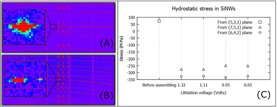
Figure 3. (Color online) (A) Before assembling into the battery cell, the single-crystalline silicon nanowires (SiNWs) were scanned by monochromatic beam to obtain Debye–Scherer pattern with theoretical silicon ring positions. The inset shows a zoomed image of diffracted peak from silicon crystal plane of (5, 3, 1) at the energy of 14.08 keV. (B) Debye–Scherer pattern is obtained from diffraction of SiNWs, after they have gone through lithiation from ~3 to 0.65 V. The inset shows a magnified image of diffracted peak from plane (6, 4, 2) at the energy of 14.62 keV. (C) Hydrostatic stress in SiNWs before the assembly of battery cell was determined from a peak, diffracted from (5, 3, 1) crystal plane as shown in (A). After assembling of battery cell, SiNWs were scanned with two different energy ranges at different levels of lithiation. Two peaks were identified from each energy range corresponding to (7, 5, 1) and (6, 4, 2) crystal planes of the crystalline part of the lithiated SiNWs. The hydrostatic stress measurement using this technique has an experimental uncertainty of about ±5 MPa (strain resolution was limited by pixel resolution in the hybrid pixel array detector in the synchrotron X-ray microdiffraction setup). Further a representative cycling (discharge) curve was presented in Figure S4 in Supplementary Material with a marking of the salient result data points presented in this manuscript.
Similarly, the hydrostatic stresses in the crystalline, cone-shaped part of the SiNWs were determined after the assembly of battery cell and during lithiation, as shown in Figure 3C. SiNWs were scanned by polychromatic μSXRD, and two diffracted peaks from the crystal planes (6, 4, 2) and (7, 5, 1) with approximate energies of 14.62 and 14.08 keV, respectively, were identified for further analysis using energy scan. The first energy scan was performed with energy from 14.56 to 14.7 keV and a step size and an exposure time of 0.002 keV and 3 s, respectively, at different levels of lithiation. Similarly, the second monochromatic scan was performed with energy from 14.02 to 14.14 keV with a step size and an exposure time of 0.002 keV and 3 s, respectively, at different levels of lithiation. Figure 3B shows an example of diffracted peak from the energy scan performed on SiNWs after they have gone through lithiation from ~3 to ~0.65 V. From the energy analysis, the peak with the highest intensity was diffracted from (6, 4, 2) crystal plane at an energy of 14.67 keV, shown in Figure 3B. The inset shows a magnified image of the reflection. It shows that the actual diffracted peak from this experiment was above the theoretically calculated silicon ring, which means dLith < dUnst. Hence, from our stress calculation, we found compressive stress of ~325.5 MPa in (6, 4, 2) crystal plane as shown in Figure 3B. This seems to be more or less the stress state of the crystalline parts of the SiNWs after lithiation as shown in Figure 3C, obtained from both the (6, 4, 2) and (7, 5, 1) crystal planes. These stress data indicate a generally compressive stress in the crystalline cores of SiNWs after lithiation. This trend is in qualitative agreement with the core–shell model during lithiation reported in the literature (Liu et al., 2012b; Zhao et al., 2012; Yang et al., 2014).
However, the stress magnitude here appears to be constant after different levels of lithiation in the experiment, while the models proposed higher and higher compressive stresses in the crystalline core of the SiNWs, reaching to high compressive stress of a few GPas (Liu et al., 2012b; Zhao et al., 2012; Yang et al., 2014). It is to be noted that in the present experiment, due to the limitation inherent of the beamline instrumentation capability at the current stage, the X-ray-focused beam (of a few microns) will shine a few SiNWs altogether, and thus the diffraction results would be an average of the few SiNWs. In addition, the core–shell models (Liu et al., 2012b; Zhao et al., 2012; Yang et al., 2014) have also indicated a stress profile with the highest compressive stresses occurring only in the inner part of the crystalline core (i.e., the inner-most few nanometers) and smaller stresses as the diameter approaches the boundary between the core and the shell parts of the SiNWs. This could lead to further averaging effects in the compressive stress state as observed in the current experiment, at least to the level of lithiation shown in Figure 3C. The SiNWs were estimated to be about 50% lithiated (with the lithiation voltage of 0.65 V) as shown in Figure 3C, based on the experimental setup of the present study.
These results seem to be comparable with previously reported stress states in silicon nanoparticles during lithiation using micro-Raman spectroscopy (Zeng et al., 2016). However, it must be noted that a micro-Raman spectroscopy technique would only examine the outer surface of the crystalline part of the silicon nanoparticles, and thus the level of stress would be as expected in the outer walls of the crystalline core of the nanoparticles, i.e., a few hundreds of MPa. This technique would not provide the complete stress distribution in the nanostructures, but could prove useful in elucidating the qualitative trend of the stress evolution during lithiation. Our present study further confirms the overall qualitative trend of the stress states of the crystalline core of the SiNWs after lithiation and could provide furthermore complete information about the stress state of different parts of the SiNWs (for instance, smaller beam could lead to finer stress information, or the white-beam data could provide deviatoric components of the stress and thus provide richer information about the stress states in the individual SiNWs). In combination, these stress studies could help further improve the understanding of the complete stress states in the SiNWs during the electrochemical lithiation and could thus lead to the design of fracture-free silicon nanostructures for next-generation LIBs.
Further, these experiments also show that the aspect ratio and spacing of the SiNWs in the electrode will have effect on the lithiation of the SiNWs. Figure 2 shows the illustrations as well as actual SEM images of the effects of the expanded LixSi beyond the spacing between the SiNWs as the electrode in the LIB. Based on these observations, short and wide SiNWs may be better compared to long and thin SiNWs, for a fixed spacing between SiNWs. However, if SiNWs are too wide, then they may pulverize (Kennedy et al., 2016).
Conclusion
In situ synchrotron scanning X-ray microdiffraction experiment was conducted to study stress states during lithiation of crystalline SiNWs in an LIB test cell. Morphological changes in the SiNWs at different levels of lithiation were also studied using SEM and compared with stress states. It was found from SEM images that lithiation predominantly began at the top of the SiNWs and progressed gradually down toward the base of the SiNWs.
The crystalline cores of the SiNWs were found to be in compressive stress (up to ~325.5 MPa) during electrochemical lithiation using in situ μSXRD. The findings of this research study help to further improve the understanding of the stress states in the SiNWs during the electrochemical lithiation and could further lead to the design of fracture-free silicon nanostructures for next-generation LIBs.
Author Contributions
Experimental work (fabrication of the samples, design and development of the battery test cell, synchrotron X-ray microdiffraction, and SEM imaging studies) was conducted by IA, ST, IR, and AA. NT and CS are synchrotron X-ray microdiffraction experts at the Advanced Light Source (ALS, Lawrence Berkeley National Laboratory, Berkeley, United States of America (USA). AB is an expert in mechanics of nanomaterials for advanced energy technologies and the principal investigator of the study. All authors contributed equally in data analysis and discussions.
Conflict of Interest Statement
The authors declare that the research was conducted in the absence of any commercial or financial relationships that could be construed as a potential conflict of interest.
Acknowledgments
We gratefully acknowledge help and support in battery cell fabrication and SiNWs samples by Prof. Carl V. Thompson’s research group, Massachusetts Institute of Technology (MIT). In particular, Thomas Peter Batcho and Wen Zheng in Prof. Carl V. Thompson’s research group at MIT are gratefully acknowledged for their assistance in sample fabrication and other experimental support. Koffi Pierre Claver Yao in the Prof. Yang Shao-Horn’s research group at MIT is also gratefully acknowledged for his assistance with the battery test cell design and fabrication. The authors also gratefully acknowledge the assistance from Dingchang Lin and Yayuan Liu from Prof. Yi Cui’s research group at the Stanford University for their assistance in the battery test cell assembly during the synchrotron experiment at Beamline 12.3.2 at ALS, Berkeley Lab. The Advanced Light Source (ALS) is supported by the Director, Office of Science, Office of Basic Energy Sciences, Materials Sciences Division, of the U.S. Department of Energy under Contract No. DE-AC02-05CH11231 at Lawrence Berkeley National Laboratory and University of California, Berkeley, CA, USA.
Supplementary Material
The Supplementary Material for this article can be found online at https://www.frontiersin.org/articles/10.3389/fenrg.2018.00019/full#supplementary-material.
References
Beaulieu, L., Eberman, K., Turner, R., Krause, L., and Dahn, J. (2001). Colossal reversible volume changes in lithium alloys. Electrochem. Solid-State Lett. 4, A137–A140. doi: 10.1149/1.1388178
Bruce, P. G., Scrosati, B., and Tarascon, J. M. (2008). Nanomaterials for rechargeable lithium batteries. Angew. Chem. Int. Ed. Engl. 47, 2930–2946. doi:10.1002/anie.200702505
Budiman, A., Besser, P., Hau-Riege, C., Marathe, A., Joo, Y.-C., Tamura, N., et al. (2009). Electromigration-induced plasticity: texture correlation and implications for reliability assessment. J. Electron. Mater. 38, 379–391. doi:10.1007/s11664-008-0602-5
Budiman, A., Hau-Riege, C., Baek, W., Lor, C., Huang, A., Kim, H., et al. (2010). Electromigration-induced plastic deformation in Cu interconnects: effects on current density exponent, n, and implications for EM reliability assessment. J. Electron. Mater. 39, 2483–2488. doi:10.1007/s11664-010-1356-4
Budiman, A., Narayanan, K. R., Li, N., Wang, J., Tamura, N., Kunz, M., et al. (2015). Plasticity evolution in nanoscale Cu/Nb single-crystal multilayers as revealed by synchrotron X-ray microdiffraction. Mater. Sci. Eng. A 635, 6–12. doi:10.1016/j.msea.2015.03.067
Budiman, A., Nix, W., Tamura, N., Valek, B., Gadre, K., Maiz, J., et al. (2006). Crystal plasticity in Cu damascene interconnect lines undergoing electromigration as revealed by synchrotron X-ray microdiffraction. Appl. Phys. Lett. 88, 233515. doi:10.1063/1.2210451
Budiman, A., Shin, H.-A.-S., Kim, B.-J., Hwang, S.-H., Son, H.-Y., Suh, M.-S., et al. (2012a). Measurement of stresses in Cu and Si around through-silicon via by synchrotron X-ray microdiffraction for 3-dimensional integrated circuits. Microelectron. Reliab. 52, 530–533. doi:10.1016/j.microrel.2011.10.016
Budiman, A. S., Lee, G., Burek, M. J., Jang, D., Han, S. M. J., Tamura, N., et al. (2012b). Plasticity of indium nanostructures as revealed by synchrotron X-ray microdiffraction. Mat. Sci. Eng. A 538, 89–97. doi:10.1016/j.msea.2012.01.017
Budiman, A. S., Han, S.-M., Li, N., Wei, Q.-M., Dickerson, P., Tamura, N., et al. (2012c). Plasticity in the nanoscale Cu/Nb single-crystal multilayers as revealed by synchrotron Laue X-ray microdiffraction. J. Mater. Res. 27, 599–611. doi:10.1557/jmr.2011.421
Chan, C. K., Peng, H., Liu, G., McIlwrath, K., Zhang, X. F., Huggins, R. A., et al. (2008). High-performance lithium battery anodes using silicon nanowires. Nat. Nanotechnol. 3, 31–35. doi:10.1038/nnano.2007.411
Chang, S. W., Chuang, V. P., Boles, S. T., Ross, C. A., and Thompson, C. V. (2009). Densely packed arrays of ultra-high-aspect-ratio silicon nanowires fabricated using block-copolymer lithography and metal-assisted etching. Adv. Funct. Mater. 19, 2495–2500. doi:10.1002/adfm.200900181
Chen, X., Dejoie, C., Jiang, T., Ku, C.-S., and Tamura, N. (2016). Quantitative microstructural imaging by scanning Laue X-ray micro-and nanodiffraction. MRS Bull. 41, 445–453. doi:10.1557/mrs.2016.97
Choi, W., Liew, T., Dawood, M., Smith, H. I., Thompson, C., and Hong, M. (2008). Synthesis of silicon nanowires and nanofin arrays using interference lithography and catalytic etching. Nano Lett. 8, 3799–3802. doi:10.1021/nl802129f
Handara, V., Radchenko, I., Tippabhotla, S., Narayanan, K. R., Illya, G., Kunz, M., et al. (2017). Probing stress and fracture mechanism in encapsulated thin silicon solar cells by synchrotron X-ray microdiffraction. Sol. Energy Mater. Sol. Cells 162, 30–40. doi:10.1016/j.solmat.2016.12.028
Kennedy, T., Brandon, M., and Ryan, K. M. (2016). Advances in the application of silicon and germanium nanowires for high-performance lithium-ion batteries. Adv. Mater. Weinheim 28, 5696–5704. doi:10.1002/adma.201503978
Kim, B.-J., Kim, J.-H., Hwang, S.-H., Budiman, A. S., Son, H.-Y., Byun, K.-Y., et al. (2012a). Microstructure evolution and defect formation in Cu through-silicon vias (TSVs) during thermal annealing. J. Electron. Mater. 41, 712–719. doi:10.1007/s11664-012-1943-7
Kim, Y., Budiman, A. S., Baldwin, J. K., Mara, N. A., Misra, A., and Han, S. M. (2012b). Microcompression study of Al–Nb nanoscale multilayers. J. Mater. Res. 27, 592–598. doi:10.1557/jmr.2011.414
Kunz, M., Tamura, N., Chen, K., MacDowell, A. A., Celestre, R. S., Church, M. M., et al. (2009). A dedicated superbend X-ray microdiffraction beamline for materials, geo-, and environmental sciences at the advanced light source. Rev. Sci. Instrum. 80, 035108. doi:10.1063/1.3096295
Lee, S.-J., Lee, J.-K., Chung, S.-H., Lee, H.-Y., Lee, S.-M., and Baik, H.-K. (2001). Stress effect on cycle properties of the silicon thin-film anode. J. Power Sources 97, 191–193. doi:10.1016/S0378-7753(01)00761-3
Lee, S. W., McDowell, M. T., Berla, L. A., Nix, W. D., and Cui, Y. (2012). Fracture of crystalline silicon nanopillars during electrochemical lithium insertion. Proc. Natl. Acad. Sci. U.S.A. 109, 4080–4085. doi:10.1073/pnas.1201088109
Lee, S. W., McDowell, M. T., Choi, J. W., and Cui, Y. (2011). Anomalous shape changes of silicon nanopillars by electrochemical lithiation. Nano Lett. 11, 3034–3039. doi:10.1021/nl201787r
Li, J.-Y., Xu, Q., Li, G., Yin, Y.-X., Wan, L.-J., and Guo, Y.-G. (2017). Research progress regarding Si-based anode materials towards practical application in high energy density Li-ion batteries. Mater. Chem. Front. 1, 1691–1708. doi:10.1039/C6QM00302H
Liu, X. H., Zheng, H., Zhong, L., Huang, S., Karki, K., Zhang, L. Q., et al. (2011). Anisotropic swelling and fracture of silicon nanowires during lithiation. Nano Lett. 11, 3312–3318. doi:10.1021/nl201684d
Liu, X. H., Zhong, L., Huang, S., Mao, S. X., Zhu, T., and Huang, J. Y. (2012a). Size-dependent fracture of silicon nanoparticles during lithiation. ACS Nano 6, 1522–1531. doi:10.1021/nn204476h
Liu, X. H., Wang, J. W., Huang, S., Fan, F., Huang, X., Liu, Y., et al. (2012b). In situ atomic-scale imaging of electrochemical lithiation in silicon. Nat. Nanotechnol. 7, 749–756. doi:10.1038/nnano.2012.170
Lukic, S. M., Cao, J., Bansal, R. C., Rodriguez, F., and Emadi, A. (2008). Energy storage systems for automotive applications. IEEE Trans. Ind. Electron. 55, 2258–2267. doi:10.1109/TIE.2008.918390
Ma, H., Cheng, F., Chen, J. Y., Zhao, J. Z., Li, C. S., Tao, Z. L., et al. (2007). Nest-like silicon nanospheres for high-capacity lithium storage. Adv. Mater. Weinheim 19, 4067–4070. doi:10.1002/adma.200700621
Ma, T., Yu, X., Li, H., Zhang, W., Cheng, X., Zhu, W., et al. (2017). High volumetric capacity of hollow structured SnO2@ Si nanospheres for lithium-ion batteries. Nano Lett. 17, 3959–3964. doi:10.1021/acs.nanolett.7b01674
MacDowell, A., Celestre, R., Tamura, N., Spolenak, R., Valek, B., Brown, W., et al. (2001). Submicron X-ray diffraction. Nucl. Instrum. Methods Phys. Res. Sect. A Accel. Spect. Detect. Assoc. Equip. 467, 936–943. doi:10.1016/S0168-9002(01)00530-7
Omar, N., Daowd, M., Bossche, P. V. D., Hegazy, O., Smekens, J., Coosemans, T., et al. (2012). Rechargeable energy storage systems for plug-in hybrid electric vehicles—assessment of electrical characteristics. Energies 5, 2952–2988. doi:10.3390/en5082952
Park, M.-H., Kim, M. G., Joo, J., Kim, K., Kim, J., Ahn, S., et al. (2009). Silicon nanotube battery anodes. Nano Lett. 9, 3844–3847. doi:10.1021/nl902058c
Peng, K., Zhang, M., Lu, A., Wong, N.-B., Zhang, R., and Lee, S.-T. (2007). Ordered silicon nanowire arrays via nanosphere lithography and metal-induced etching. Appl. Phys. Lett. 90, 163123. doi:10.1063/1.2724897
Radchenko, I., Tippabhotla, S. K., Tamura, N., and Budiman, A. S. (2016). Probing phase transformations and microstructural evolutions at the small scales: synchrotron X-ray microdiffraction for advanced applications in 3D IC (integrated circuits) and solar PV (photovoltaic) devices. J. Electron. Mater. 45, 6222–6232. doi:10.1007/s11664-016-5012-5
Rengarajan, K. N., Radchenko, I., Illya, G., Handara, V., Kunz, M., Tamura, N., et al. (2016). Low stress encapsulants? Influence of encapsulation materials on stress and fracture of thin silicon solar cells as revealed by synchrotron X-ray submicron diffraction. Procedia Eng. 139, 76–86. doi:10.1016/j.proeng.2015.09.230
Ryu, I., Choi, J. W., Cui, Y., and Nix, W. D. (2011). Size-dependent fracture of Si nanowire battery anodes. J. Mech. Phys. Solids 59, 1717–1730. doi:10.1016/j.jmps.2011.06.003
Saw, L. H., Ye, Y., and Tay, A. A. (2016). Integration issues of lithium-ion battery into electric vehicles battery pack. J. Cleaner Prod. 113, 1032–1045. doi:10.1016/j.jclepro.2015.11.011
Shelke, M. V., Gullapalli, H., Kalaga, K., Rodrigues, M. T. F., Devarapalli, R. R., Vajtai, R., et al. (2017). Facile synthesis of 3D anode assembly with si nanoparticles sealed in highly pure few layer graphene deposited on porous current collector for long life Li-ion battery. Adv. Mater. Interfaces 4:1601043. doi:10.1002/admi.201601043
Shim, H. C., Woo, C.-S., and Hyun, S. (2016). “Silicon-carbon nanotube aerogel core-shell nanostructures for lithium-ion batteries with long-cycle life and high capacity,” in Meeting Abstracts, Vol 3 (The Electrochemical Society), 276–276.
Tamura, N. (2014). “XMAS: A versatile tool for analyzing synchrotron X-ray microdiffraction data,” in Strain and Dislocation Gradients from Diffraction: Spatially-Resolved Local Structure and Defects, eds R. Barabash and G. Ice (Hackensack: World Scientific), 125–155.
Tippabhotla, S. K., Radchenko, I., Song, W.J.R., Illya, G., Handara, V., Kunz, M., et al. (2017a). From cells to laminate: probing and modeling residual stress evolution in thin silicon photovoltaic modules using synchrotron X-ray micro-diffraction experiments and finite element simulations. Prog. Photovoltaics Res. Appl. 25, 791–809. doi:10.1002/pip.2891
Tippabhotla, S. K., Radchenko, I., Stan, C. V., Tamura, N., and Budiman, A. (2017b). “Enabling the study of stress states using in situ µSXRD in the silicon nanowire anode during electrochemical lithiation in a specially designed Li-ion battery test cell,” in Procedia Engineering ICMAT.
Wu, H., Chan, G., Choi, J. W., Ryu, I., Yao, Y., McDowell, M. T., et al. (2012). Stable cycling of double-walled silicon nanotube battery anodes through solid-electrolyte interphase control. Nat. Nanotechnol. 7, 310–315. doi:10.1038/nnano.2012.35
Yang, H., Fan, F., Liang, W., Guo, X., Zhu, T., and Zhang, S. (2014). A chemo-mechanical model of lithiation in silicon. J. Mech. Phys. Solids 70, 349–361. doi:10.1016/j.jmps.2014.06.004
Yang, H., Huang, S., Huang, X., Fan, F., Liang, W., Liu, X. H., et al. (2012). Orientation-dependent interfacial mobility governs the anisotropic swelling in lithiated silicon nanowires. Nano Lett. 12, 1953–1958. doi:10.1021/nl204437t
Zeng, Z., Liu, N., Zeng, Q., Lee, S. W., Mao, W. L., and Cui, Y. (2016). In situ measurement of lithiation-induced stress in silicon nanoparticles using micro-Raman spectroscopy. Nano Energy 22, 105–110. doi:10.1016/j.nanoen.2016.02.005
Zhang, S., Du, Z., Lin, R., Jiang, T., Liu, G., Wu, X., et al. (2010). Nickel nanocone-array supported silicon anode for high-performance lithium-ion batteries. Adv. Mater. Weinheim 22, 5378–5382. doi:10.1002/adma.201003017
Zhao, K., Pharr, M., Wan, Q., Wang, W. L., Kaxiras, E., Vlassak, J. J., et al. (2012). Concurrent reaction and plasticity during initial lithiation of crystalline silicon in lithium-ion batteries. J. Electrochem. Soc. 159, A238–A243. doi:10.1149/2.020203jes
Keywords: in situ, lithium-ion battery, single-crystalline silicon nanowires, lithiation, stress, deformation, synchrotron X-ray microdiffraction
Citation: Ali I, Tippabhotla SK, Radchenko I, Al-Obeidi A, Stan CV, Tamura N and Budiman AS (2018) Probing Stress States in Silicon Nanowires During Electrochemical Lithiation Using In Situ Synchrotron X-Ray Microdiffraction. Front. Energy Res. 6:19. doi: 10.3389/fenrg.2018.00019
Received: 09 January 2018; Accepted: 05 March 2018;
Published: 04 April 2018
Edited by:
Xiangming H. E., Tsinghua University, ChinaReviewed by:
Liqiang Mai, Wuhan University of Technology, ChinaShaomao Xu, University of Maryland, College Park, United States
Bin Liu, Pacific Northwest National Laboratory (DOE), United States
Zhiqiang Wang, University of Western Ontario, Canada
Copyright: © 2018 Ali, Tippabhotla, Radchenko, Al-Obeidi, Stan, Tamura and Budiman. This is an open-access article distributed under the terms of the Creative Commons Attribution License (CC BY). The use, distribution or reproduction in other forums is permitted, provided the original author(s) and the copyright owner are credited and that the original publication in this journal is cited, in accordance with accepted academic practice. No use, distribution or reproduction is permitted which does not comply with these terms.
*Correspondence: Arief Suriadi Budiman, c3VyaWFkaUBhbHVtbmkuc3RhbmZvcmQuZWR1