 Dezhao Li
 Yang Li
 Yu Su
Yu Su Cheng Chi
 Baoling Huang
- 1Department of Mechanical and Aerospace Engineering, The Hong Kong University of Science and Technology, Kowloon, Hong Kong
- 2The Hong Kong University of Science and Technology Shenzhen Research Institute, Shenzhen, China
An ultra-broadband selective absorber has been realized with a hierarchical structure through integrating vacuum impedance-matched structure, quarter wavelength structure, and gradient refractive index structure. Through optimizing the design parameters of the proposed hierarchical structure, an ultra-broadband infrared absorber covering the three major atmospheric windows (0.7–2.5, 3–5, and 8–14 μm) has been numerically and experimentally demonstrated. An overall absorption up to 80% covering all the three major atmospheric infrared windows and a ratio of the total absorptions within and beyond the windows as high as 5.88 has been achieved with the developed absorber. The high absorption and spectral selectivity of the absorber make it promising for sensitive broadband infrared spectroscopy detection. The proposed hierarchical structure also provides great design freedom with many tunable factors, making it convenient to extend the design for other applications. In addition, we developed a cost-effective lithography-free method for the fabrication of this structure. The design flexibility and fabrication convenience of this hierarchical structure render it suitable for the development of tailored selective broadband absorbers for targeted applications.
Introduction
Infrared (IR), a type of electromagnetic radiation with a wavelength ranging from 0.7 µm to 1 mm, has been widely applied in many areas such as gas sensing (Sun et al., 2016), photovoltaics (Gan et al., 2013), environmental monitoring (Rauste et al., 1997), medical testing (Liu et al., 2015), and so on. Due to the existence of dusts and various greenhouse gases including water vapor in the atmosphere, IR devices typically utilize one of the three major infrared windows, i.e., the near-infrared (NIR), 0.7–2.5 μm, mid-infrared (MIR), 3–5 μm, and far-infrared (FIR), 8–14 μm atmospheric transmission windows, within which electromagnetic wave can travel through the air without much absorption. A key component influencing the performance of an infrared device is the infrared absorber. Different from black body absorbers (Yang et al., 2008; Mizuno et al., 2009) with uniform absorption over a wide spectrum, selective broadband infrared absorbers with strong absorption in targeted wide bands and much weaker absorption in other regimes, can help to maximize the energy conversion efficiency of solar-thermal systems (Li et al., 2015) and improve the detectivities of infrared sensors by reducing the background radiation noise (Talghader et al., 2012), therefore, attracting great interest in recent decades. Selective broadband absorbers include metamaterials utilizing the excitation of the surface plasmon resonance (Ji et al., 2014; Guo et al., 2016; Wu, 2016), and impedance-matched multilayer structures (Corrigan et al., 2012; Mattiucci et al., 2013; Deng et al., 2015; Yang et al., 2016), have been widely investigated. Wu (2016) proposed and numerically demonstrated a multilayer grating structure with an absorption of above 90% from 2,749 to 4,966 nm. Ji et al. (2014) developed a patterned hyperbolic metafilm based on multilayer metamaterial waveguide taper with a tunable absorption band from NIR to MIR. Guo et al. (2016) numerically demonstrated an ultra-broadband infrared absorber based on metasurface that could achieve an absorption over 80% in the MIR region between 5.2 and 13.7 µm. However, these metamaterial selective broadband absorbers usually require expensive patterning or complicated fabrication techniques such as e-beam lithography, focused ion beam milling, and nanolithography. For large-scale practical applications, people proposed multilayer absorbers through matching the structure impedance to the free space impedance, and efficient absorbers covering the NIR (0.7–1.3 μm) region have been realized (Deng et al., 2015). Absorbers with even broader band absorption (~98% over the region of 0.4–2 μm) based on the tandem structures with graded refractive index have been reported (Yang et al., 2016). So far, however, broadband absorbers that can selectively cover all the three IR regimes (NIR, MIR, and FIR) have been rarely explored, which can maximize the IR energy absorption/emission and reduce the noise from background radiation or the interference from other IR sources nearby.
To provide a tunable and ultra-broadband selective absorber design that can cover all the three absorption regions, integrating multiple absorption mechanisms is a natural idea. Corrigan et al. (2012) conducted a theoretical analysis on the feasibility of combining an antireflective structure and a quarter wavelength (QW) structure. Here, we present a hierarchical structure suitable for mass production by integrating an impedance-matched (IM) structure, a QW structure, and a gradient refractive index (GRI) structure to construct selective broadband IR absorbers. A lithography-free IC-compatible fabrication process has been developed to produce this structure. As an embodiment of this design, an ultra-broadband (covering wavelength region 0.7–14 μm) selective IR absorber with a spectral absorption matching with the three major IR atmospheric transmission windows, was developed. Using the same strategy, various selective broadband absorbers for different spectrum regions can also be readily realized, making it attractive for many applications including the energy harvesting, infrared detection, thermal shielding, and so on.
Structure Design and Fabrication
An IM structure (Deng et al., 2015; Peng et al., 2016) utilizes a specially designed dielectric and metal stack layer to match the structure impedance to the free space value, therefore, allowing the light with a specific wavelength to be absorbed by the interval metal layer while penetrating into the whole structure with little reflection. A QW structure (Parsons and Pedder, 1988) can decrease the reflection within a certain wavelength region and result in a higher absorption, while the absorption region depends on the intrinsic refractive index properties of the adopted material. A GRI structure (Huang et al., 2007) can suppress the reflection in a broad wavelength region owing to various heights of the sub-wavelength structures. To integrate those structures for ultra-broadband absorption, a general design strategy considering their different spectral properties is proposed here. Since the IM structure (Mattiucci et al., 2013) is usually applied for short wavelength regions from UV to NIR, with metal as its absorption layer, it should be placed as the bottom structure as shown in Figure 1, because it can also block the MIR and FIR light. To extend the absorption region, the QW structure with a dielectric layer that can absorb MIR and FIR but allow UV and NIR to pass through freely, may be placed above the IM structure. Since the hierarchical structure’s absorption is also limited by the surface reflection, an effective antireflective structure can help to decrease the reflection and increase the overall absorption. The GRI structure can be used as antireflective coating for any material (Chattopadhyay et al., 2010). The gradual transition of the effective refractive index in the GRI structure leads to a small reflection and makes it an ideal choice for the top layer, as shown in Figure 1.
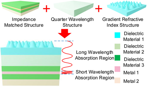
Figure 1. Scheme of the hierarchical structure of the tunable broadband absorber consisting of an impedance-matched structure, a quarter wavelength structure, and a gradient refractive index structure.
The structure optimization was started with the bottom IM structure shown in Figure 2A. The effective wave impedance of the structure consisting of a metal layer (with complex refractive index Nm) embedded between two dielectric layers (with the refractive index nd, and extinction coefficient kd ≈ 0) on a thick metal substrate (with the complex refractive index Nbase), can be described as (Haus, 1984; Deng et al., 2015):
where M and D are the phase shifts in the metal and dielectric layers with M = κ0Nmdm and D = κ0Ndd (dm and d are the thicknesses of the metal and dielectric layers, respectively), and κ0 is the wave number in vacuum. To achieve a high absorption for the targeted wavelength region, the effective impedance of this structure Zeff should be close to the free space impedance (Mattiucci et al., 2013; Deng et al., 2015) Z0, i.e., Zeff ≈ Z0, and the thickness of the interval metal layer dm should be less than its skin depth , where c is the light velocity, ρ is the electrical resistivity of metal, μ is the relative permeability of metal. Comparing with the optical wavelength, the metal thickness is ultrathin, i.e., κ0dm << 1. To obtain a broadband absorption region for our target wavelength region, 40-nm-thick lossy type metal (Peng et al., 2016), titanium was chosen as the interval metal layer. For a given metal layer, M is constant, according to Eq. 1, and the absorption properties will be periodically changed with the variation in D, which is directly related to the dielectric layer thickness d.
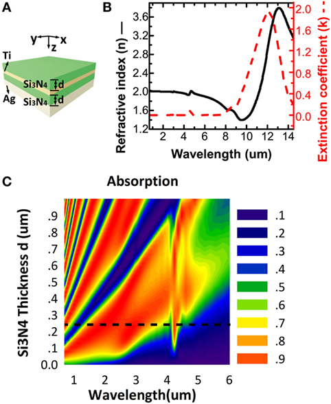
Figure 2. (A) Schematic of the impedance-matched structure. (B) The measured optical constants of the Si3N4 layer deposited by plasma-enhanced chemical vapor deposition. (C) The simulated absorption of the impedance-matched structure with respect to the Si3N4 layer thickness.
For a broadband tunable region (0.7–5 µm), we selected Si3N4 as the dielectric layer material, because it has a relatively high refractive index n (Palik and Ghosh, 1998) and is easy to deposit. Meanwhile, silver is reported to have a high reflection (Palik and Ghosh, 1998) over a wide wavelength range, making it an ideal choice for the bottom reflection layer (Figure 2A).
Usually, the optical properties of a dielectric material vary with different deposition processes. We measured the optical constants of the Si3N4 layer deposited by the plasma-enhanced chemical vapor deposition (PECVD) method, as shown in Figure 2B, with a J.A. Woollam Multi-Wavelength Ellipsometer and Fourier-transform infrared spectroscopy (FTIR) (Rocha and Pilling, 2014). With the measured optical properties of the thin film materials, numerical calculation was conducted using the 3D FDTD simulation method (FDTD solutions v8.16, Lumerical) to obtain the absorption of the IM structure. A plane wave was incident to the top surface of the IM structure along the x-direction with the simulation region defined by the periodic boundaries along the x- and y-direction and the perfectly matching layers boundary along the z-direction, as shown in Figure 2A. While keeping other parameters unchanged, we calculated the spectral absorption results of the IM structure with different Si3N4 layer thicknesses, as shown in Figure 2C. According to the simulation results, the Si3N4 layer thickness d was selected to be 250 nm for further optimization.
The QW structure was then integrated with the optimized IM structure for the absorption of longer wavelength light. To minimize the influence of the added QW structure to the designed IM structure, we choose the same dielectric material Si3N4, which shows good absorption in the region from 8 to 14 µm and is nearly transparent for UV and NIR, for the QW structure optimization. To get a high absorption, the total Si3N4 thickness Dt, shown in Figure 3A, should meet the requirement:
where λT is the center wavelength of targeted FIR region and m is an integer. Meanwhile, it is necessary to evaluate how the added Si3N4 layer will influence the behavior of the underneath IM structure. The IM structure makes use of the phase shifts M and D in the metal and dielectric layers. Since the phase shift is periodic changed when the material thickness increases, as long as the total thickness of the added Si3N4 layer is an integral multiple of that of the IM structure designed, i.e., Dt = ad where a is any integer, the absorption of the designed IM structure will not be significantly affected. Since the targeted wavelength band of the QW structure is from 8 to 14 µm with the center wavelength around 11 µm and the refractive index of Si3N4 is around 2.5, the optimal thickness Dt is 1.25 µm, around five times that part of the IM structure.
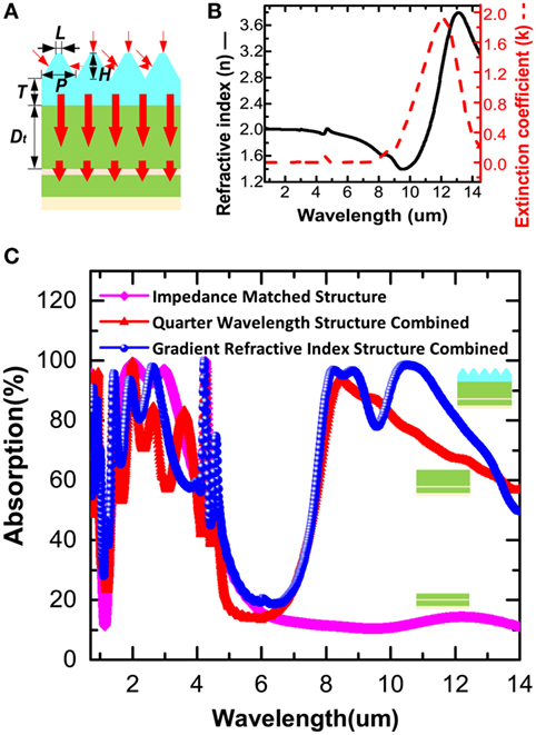
Figure 3. (A) Schematic of the light propagation in the hierarchical structure. (B) Measured optical constants of the SiO2 layer deposited by the plasma-enhanced chemical vapor deposition method at room temperature. (C) Simulated absorption properties of the integrated IM + QW structure and the finial optimized hierarchical structure.
Decreasing the structure’s reflection can further improve the absorption and, therefore, an antireflective structure (Steglich et al., 2015) can be adopted. The optimized antireflective structure should satisfy the condition , where na, ni, and ns are the refractive indexes of the antireflective layer, air, and substrate material under the antireflective layer, respectively. Since the refractive index of the material under the antireflective layer is around 2.5 for Si3N4 for the targeted region 8–14 μm in our case, we selected PECVD SiO2 deposited at low temperature (25°C), which has a matching reflective index of around 1.6, shown in Figure 3B, as the material of the antireflective layer. In addition, the extinction coefficient of SiO2 indicates it can enhance the absorption near 10 µm, as shown in Figure 3B.
To realize a better antireflective property, the GIR structure is expected to be an ideal choice (Perl et al., 2014). The effective index on the interface is neff = fna, where f is the volume ratio between the material and air; therefore, the effective index can be tuned by varying the volume ratio f despite the material’s intrinsic property. With the refractive index of SiO2 and targeted absorption wavelength, the optimal thickness of SiO2 is around 1 µm, according to Eq. 2. Further optimization was performed with the FDTD software, and the simulations revealed that the optimal flat layer thickness T of the SiO2 GRI structure is 500 nm, and that of top pyramid structure H is 500 nm, while the optimal period P is ~100 nm and the tip diameter L is ~50 nm. The simulated absorption results for the integrated heterostructure are shown in Figure 3C, which indicate multi-band selective absorber can be realized by simply “adding” structures with different absorption bands. The decoupling of the substructures in the heterostructure makes it easy to optimize the selective ultrabroadband absorber and extend it for other applications.
Even though the GRI structure is considered to be an ideal choice for the reflection reduction, a mass-producible fabrication of such structures is tricky. We developed a lithography-free fabrication technique by making use of the special oxygen plasma etching profile of the silicon-containing polyimide (PI) (Tsang et al., 1996), as shown in Figure 4A.
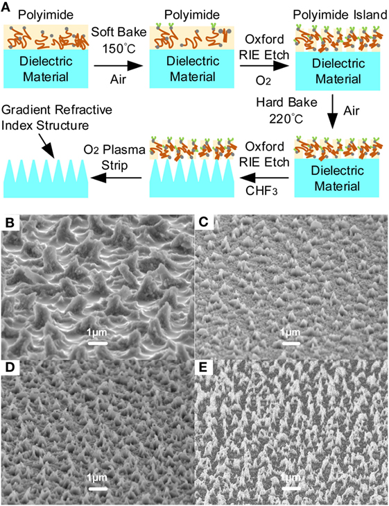
Figure 4. (A) Fabrication process flow for the gradient refractive index structure. The SEM pictures of different patterns generated using reactive ion etching (RIE). (B) with a plasma power of 100 W and 100 sccm O2, (C) with a plasma power of 100 W and 50 sccm O2, (D) with a plasma power of 50 W and 50 sccm O2, and (E) with a plasma power of 50 W and 100 sccm O2.
First, a thin layer of PI2525 from DuPont was spin coated on the top surface. After pre-baking (at 150°C) for 5 min, a thin SiO2 layer was formed at the PI surface, which will help to generate uniform patterns. After that, the sample was etched in oxygen plasma with the reactive ion etching (RIE). Because of the competition between the oxide layer formation in oxygen environment and its damage by the ion plasma, the density and morphology of the patterns can be controlled by tuning the oxygen flow rate and the plasma power. After the patterns were generated, the samples were hard baked at 220°C for 5 min, and then the generated patterns were used as masks to etch away the SiO2 in the CF3H gas environment with RIE to form the GRI structure. Finally, the polymer residues were removed using oxygen plasma, and the SEM images of those patterns produced with different combinations of oxygen flow rate and plasma power were shown in Figures 4B–E. Our tests showed that through tuning the oxygen plasma etching power and time, the diameters of the pillars can be controlled in a range from 0.05 to 1 µm while the spacing can be controlled in a range from 0.1 to 2 µm.
With this carefully controlled pattern generation process, we finally generated a hierarchical structure with the optimal structural parameters and the SEM pictures of the top view and side view of the structure are shown in Figures 5A,B. The reflectance is measured with the FTIR (Vertex 70 Hyperion 1000). The measured and simulated spectral absorption results are presented in Figure 5C, showing good agreements with each other. It can be seen that the spectral absorption is in accord with the three major atmospheric IR transmission windows, showing much weaker absorption beyond the three windows.
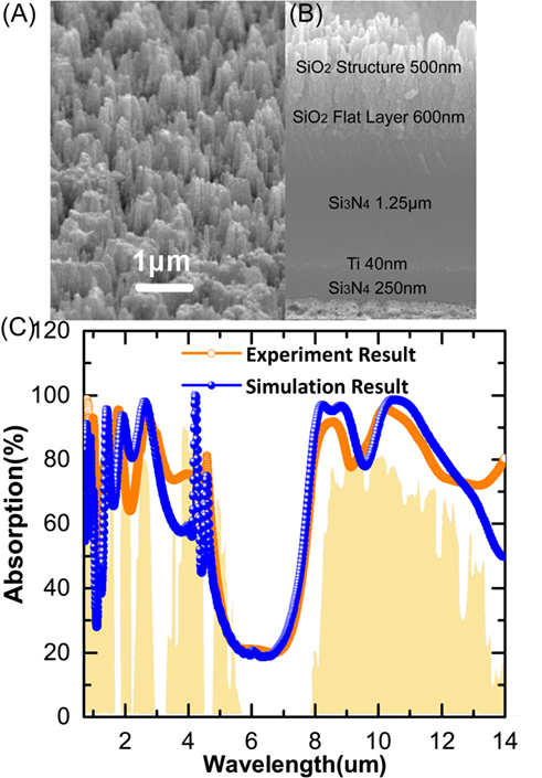
Figure 5. SEM pictures of (A) the top view and (B) the side view of the fabricated structure. (C) The simulated and experimental absorption results of the optimized hierarchical structure, in comparison with the atmospheric transmission spectra from 0.7 to 14 µm.
To evaluate the absorption and selectivity of the absorber, we defined two parameters, the effective absorption Aa and the broadband spectral selectivity R,
where a(λ) is the absorption value corresponding to special wavelength, Aa is the total absorption efficiency covering the three atmospheric windows. The effective absorption evaluates the average absorbance in the three major IR windows while R indicates the relative strength of useful absorption to the undesired absorption over the entire IR regime. Apparently, single band selective absorber will have a low Aa value. For full band perfect absorber, such as black metal, the total absorption efficiency can be over 90% while the spectral selectivity is around 2.8. In contrast, our fabricated absorber can offer a total absorption efficiency of 80% and a selectivity R of 5.88, showing much better broadband selective absorption.
Conclusion
In conclusion, a mass producible hierarchical structure for selective broadband absorber has been proposed and experimentally demonstrated. The developed selective broadband absorber, covering all the atmospheric transmission windows in the wavelength range from 0.7 to 14 µm, can achieve an overall absorption up to 80% and a spectral selectivity of 5.88.
The integration of multiple absorption mechanisms is proved to be efficient for tailoring the broadband absorption. A hierarchical structure integrating IM, QW, and GRI structures has been demonstrated for ultrabroadband selective absorber applications. Following similar integration strategy, the three structures can also be individually tailored for other applications. To extend this hierarchical design for other targeted wavelength regions, it is very important to choose suitable material with favorable refractive indexes and extinction coefficients.
The proposed design can be potentially used in other applications such as smart building, passive radiation cooler, which need wide electromagnetic spectrum absorption regions. Current absorber has a relatively high absorption in the visible light region. Future improvement can be made by adopting reflection layer for visible light. The relative independence and tunability of each substructure provide flexibility in tailoring this design for other relevant applications.
In principle, other kinds of polymers containing silicon ions can also be adopted for the patterning with this fabrication process. However, since the effects of the soft-baking process and the etching process on the polymer chains are dependent on the polymer structure, which may result in different pillar patterns, the fabrication recipes for different polymers should be tuned to achieve the best results.
Author Contributions
DL contributed to the experiments design, performed the experiments, and drafted the manuscript. YL contributed to the experiments design and data collection. YS and CC analyzed and interpreted the data. BH supervised the research and revised the manuscript.
Conflict of Interest Statement
The authors declare that the research was conducted in the absence of any commercial or financial relationships that could be construed as a potential conflict of interest.
Funding
We are thankful for the financial support from the Hong Kong Research Grant Council via the Collaborative Research Fund (Grant No. C6022-16G) and the Hong Kong General Research Fund (Grant No. 16213015).
References
Chattopadhyay, S., Huang, Y. F., Jen, Y. J., Ganguly, A., Chen, K. H., and Chen, L. C. (2010). Anti-reflecting and photonic nanostructures. Mater. Sci. Eng. R Rep. 69, 1–35. doi: 10.1016/j.mser.2010.04.001
Corrigan, T. D., Park, D. H., Drew, H. D., Guo, S. H., Kolb, P. W., Herman, W. N., et al. (2012). Broadband and mid-infrared absorber based on dielectric-thin metal film multilayers. Appl. Opt. 51, 1109–1114. doi:10.1364/Ao.51.001109
Deng, H. X., Li, Z. G., Stan, L., Rosenmann, D., Czaplewski, D., Gao, J., et al. (2015). Broadband perfect absorber based on one ultrathin layer of refractory metal. Opt. Lett. 40, 2592–2595. doi:10.1364/Ol.40.002592
Gan, Q. Q., Bartoli, F. J., and Kafafi, Z. H. (2013). Plasmonic-enhanced organic photovoltaics: breaking the 10% efficiency barrier. Adv. Mater. Weinheim 25, 2385–2396. doi:10.1002/adma.201203323
Guo, W. L., Liu, Y. X., and Han, T. C. (2016). Ultra-broadband infrared metasurface absorber. Opt. Express 24, 20586–20592. doi:10.1364/Oe.24.020586
Huang, Y. F., Chattopadhyay, S., Jen, Y. J., Peng, C. Y., Liu, T. A., Hsu, Y. K., et al. (2007). Improved broadband and quasi-omnidirectional anti-reflection properties with biomimetic silicon nanostructures. Nat. Nanotechnol. 2, 770–774. doi:10.1038/nnano.2007.389
Ji, D. X., Song, H. M., Zeng, X., Hu, H. F., Liu, K., Zhang, N., et al. (2014). Broadband absorption engineering of hyperbolic metafilm patterns. Scientific Reports 4, 4498. doi:10.1038/srep04498
Li, P. F., Liu, B. A., Ni, Y. Z., Liew, K. K., Sze, J., Chen, S., et al. (2015). Large-scale nanophotonic solar selective absorbers for high-efficiency solar thermal energy conversion. Adv. Mater. Weinheim 27, 4585–4591. doi:10.1002/adma.201501686
Liu, R., Wang, J., and Liu, J. (2015). Thermal infrared images to quantify thermal ablation effects of acid and base on target tissues. AIP Adv. 5, 077176. doi:10.1063/1.4927762
Mattiucci, N., Bloemer, M. J., Akozbek, N., and D’Aguanno, G. (2013). Impedance matched thin metamaterials make metals absorbing. Sci. Rep. 3, 3203. doi:10.1038/srep03203
Mizuno, K., Ishii, J., Kishida, H., Hayamizu, Y., Yasuda, S., Futaba, D. N., et al. (2009). A black body absorber from vertically aligned single-walled carbon nanotubes. Proc. Natl. Acad. Sci. U.S.A. 106, 6044–6047. doi:10.1073/pnas.0900155106
Palik, E. D., and Ghosh, G. (1998). Handbook of Optical Constants of Solids. San Diego: Academic Press.
Parsons, A. D., and Pedder, D. J. (1988). Thin-film infrared absorber structures for advanced thermal detectors. J. Vacuum Sci. Technol. A 6, 1686–1689. doi:10.1116/1.575308
Peng, H., Luo, Y., Ying, X. X., Pu, Y., Jiang, Y. D., Xu, J. M., et al. (2016). Broadband and highly absorbing multilayer structure in mid-infrared. Appl. Opt. 55, 8833–8838. doi:10.1364/Ao.55.008833
Perl, E. E., McMahon, W. E., Bowers, J. E., and Friedman, D. J. (2014). Design of antireflective nanostructures and optical coatings for next-generation multijunction photovoltaic devices. Opt. Express 22, A1243–A1256. doi:10.1364/Oe.22.0a1243
Rauste, Y., Herland, E., Frelander, H., Soini, K., Kuoremaki, T., and Ruokari, A. (1997). Satellite-based forest fire detection for fire control in boreal forests. Int. J. Remote Sen. 18, 2641–2656. doi:10.1080/014311697217512
Rocha, W. R. M., and Pilling, S. (2014). Determination of optical constants n and k of thin films from absorbance data using Kramers-Kronig relationship. Spectrochim. Acta A Mol. Biomol. Spectros. 123, 436–446. doi:10.1016/j.saa.2013.12.075
Steglich, M., Kasebier, T., Schrempel, F., Kley, E. B., and Tunnermann, A. (2015). Self-organized, effective medium Black Silicon for infrared antireflection. Infrared Phys. Technol. 69, 218–221. doi:10.1016/j.infrared.2015.01.033
Sun, J., Deng, H., Liu, N. W., Wang, H. L., Yu, B. L., and Li, J. S. (2016). Mid-infrared gas absorption sensor based on a broadband external cavity quantum cascade laser. Rev. Sci. Instrum. 87, 123101. doi:10.1063/1.4968041
Talghader, J. J., Gawarikar, A. S., and Shea, R. P. (2012). Spectral selectivity in infrared thermal detection. Light Sci. Appl. 1, e24. doi:10.1038/lsa.2012.24
Tsang, Y. L., Miller, C., and Lii, T. (1996). Investigation of polyimide residue due to reactive ion etching in O-2. J. Electrochem. Soc. 143, 1464–1469. doi:10.1149/1.1836660
Wu, J. (2016). Broadband light absorption by tapered metal-dielectric multilayered grating structures. Opt. Commun. 365, 93–98. doi:10.1016/j.optcom.2017.12.006
Yang, C. Y., Ji, C. G., Shen, W. D., Lee, K. T., Zhang, Y. G., Liu, X., et al. (2016). Compact multilayer film structures for ultrabroadband, omnidirectional, and efficient absorption. ACS Photonics 3, 1332–1332. doi:10.1021/acsphotonics.6b00395
Keywords: ultra-broadband infrared absorber, atmospheric windows matching, hierarchical structure, lithography-free, tunable absorber
Citation: Li D, Li Y, Su Y, Chi C and Huang B (2018) Atmospheric-Window-Matching Hierarchical Broadband Infrared Absorber Realized by Lithography-Free Fabrication. Front. Energy Res. 6:20. doi: 10.3389/fenrg.2018.00020
Received: 17 December 2017; Accepted: 09 March 2018;
Published: 26 March 2018
Edited by:
Qing Hao, University of Arizona, United StatesReviewed by:
Tandeep Singh Chadha, Applied Particle Technology, LLC, United StatesShuang Tang, SUNY Polytechnic Institute, United States
Copyright: © 2018 Li, Li, Su, Chi and Huang. This is an open-access article distributed under the terms of the Creative Commons Attribution License (CC BY). The use, distribution or reproduction in other forums is permitted, provided the original author(s) and the copyright owner are credited and that the original publication in this journal is cited, in accordance with accepted academic practice. No use, distribution or reproduction is permitted which does not comply with these terms.
*Correspondence: Baoling Huang, bWViaHVhbmdAdXN0Lmhr