 Mikimasa Katayama1
 Toshihiko Kaji
- 1Department of Applied Physics, Tokyo University of Agriculture and Technology, Tokyo, Japan
- 2Department of Materials Molecular Science, Institute for Molecular Science, Okazaki, Japan
Organic optoelectronic devices tend to have limited thickness. Organic light emitting diodes (OLED) and organic photovoltaic cells (OPV) made of organic pigments are typically with thickness of a few or a few tens of nanometers. Thickness of organic photovoltaic cells made with polymers exceeds them typically up to the order of a few 100 nm but still necessarily co-optimized with respect to light absorption and charge transport. Here, we demonstrate that crystallization made a 10-μm-thick pigment layer active in a photovoltaic cell, using a prototypical pair of pigments, phthalocyanine, and fullerene. It is proved that crystalline pigment layer with a thickness much greater than what is needed for optical optimization can be utilized for organic optoelectronic devices and that organic optoelectronic devices have potentiality to relief their design from co-optimization of optics and charge transport.
Introduction
Organic photovoltaic (OPV) cells have achieved a power conversion efficiency >10%, a level of performance deemed suitable for solar energy conversion applications (Søndergaard et al., 2012; Dou et al., 2013; Kang et al., 2016; Meng et al., 2018). In addition, they offer advantages over conventional crystalline silicon photovoltaic cells because of their light weight and manufacturability on flexible plastic substrates. Since the discovery of OPVs based on heterojunction and bulk-heterojunction layer structures, various approaches have been successfully adopted to optimize the power conversion efficiency, ranging from the design and screening of materials (Mishra and Bäuerle, 2012; Roncali et al., 2014; Meng et al., 2018) and fine-tuning of the thin film deposition processes (Kaji et al., 2011; Song et al., 2014) to the control of the cell's layer structures (Riede et al., 2011; Luo et al., 2016). Often the optimization process involves trade-offs among key cell parameters, such as layer composition and thickness. For instance, the optical absorption of the active layer, i.e., optoelectronic conversion layer, can be enhanced by increasing the layer thickness but only to a certain extent, beyond which, recombination and transport of photo-generated charges through the active layer are the controlling factors for photocurrent generation rather than light absorption. Thus, to enhance the photocurrent at zero bias, short-circuit current Jsc, the thickness of the active layer is often designed to take advantage of various standing waves for optimal utilization of incident photons without incurring limitations due to charge recombination and transport (Pfuetzner et al., 2009; Zhou et al., 2012). An active layer with a thickness of 40 nm is often optimal for vacuum-deposited OPV cells made of pigments in conjunction with the first standing waves (Xue et al., 2005; Schueppel et al., 2010; Zhou et al., 2012; Wang et al., 2014) although light absorption is far from adequate. Utilization of the second and third standing waves can produce enhanced absorption. In the design of tandem OPV cells, the bottom cell is often positioned at around 200 nm from the metal (reflecting) electrode to benefit from the second standing wave (Schueppel et al., 2010; Ko et al., 2016; Meng et al., 2018). Thicker active layers can be used in OPV cells made with polymers; the optimal range is approximately 300 nm where the antinode of the third standing wave is located. Beyond this thickness, the efficiency of such polymer cells tends to decrease (Osaka et al., 2014; Jung et al., 2015; Ko et al., 2016) or stop increasing (Jin et al., 2016; Ko et al., 2016) owing to the reduction of both Jsc and the fill factor, FF.
In a few exceptional cases, OPV cells could produce high Jsc with an extraordinarily thick active layer of 1 μm (Sakai and Hiramoto, 2008; Price et al., 2011; Osaka et al., 2014). This unusual behavior has been reported for both vacuum-deposited small-molecule pigment (Sakai and Hiramoto, 2008) and solution-coated polymer OPV cells (Price et al., 2011; Osaka et al., 2014). In these cases, however, the relationship among Jsc, the light absorption of the active layer, and the optical effect of the standing waves has not been clarified. In this study, we demonstrate that both high Jsc and FF can be achieved in a prototypical ZnPc:C60 OPV cell using an active layer of thickness up to 10 μm, which is an order of magnitude larger than what has been reported and certainly much beyond what is commonly needed for light absorption optimization, such as utilizing the third standing wave or a textured substrate. Most remarkably, high performance of OPV cells can be maintained throughout a wide range of thicknesses (0.04–10 μm) for the active layer. This result can be attributed to the effects of crystallization of the active layer and, to a lesser extent, the use of various interface layers in constructing and reproducing the OPV cells.
Materials and Methods
Materials and Substrates
C60 (Frontier Carbon) and ZnPc (Tokyo Chemical Industry) were purified by conventional entrainer sublimation. We used a custom-designed purification system (Epitec) equipped with a three-zone infrared heating furnace (Thermo Riko) under the optimized pressures of 5–15 kPa. F4TCNQ (>98%, Tokyo Chemical Industry), CuI (99.999%, Aldrich), Alq3 (>98%, Tokyo Chemical Industry), and LiF (Alfa Aesar) were used as is without further purification. PDMS (polydimethylsiloxane, Shin-Etsu Silicones, KF96-50cs) was also used as is, which chain length n is around 41 and molecular weight is around 3,203 g/mol on average. ITO (150 nm, 10 Ω/cm2) and FTO (600–800 nm, 8 Ω/cm2, TCO VU, AGC) glass substrates (0.7 mm) were patterned by Techno Print.
OPV Cell Fabrication
ITO and FTO substrates were treated by air-plasma in PIB-20 Ion-bombarder (Vacuum Device). Vacuum deposition was carried out in a custom-designed vacuum chamber (Katagiri Engineering/M&Y System) equipped with a turbo molecular pump. Typical vacuum during the deposition was 1 × 10⁻³ Pa. After introducing the substrates into the vacuum chamber, the entire cell fabrication process was completed without exposing them to the air. All vacuum chambers were equipped with oil-free vacuum pumps.
Film thicknesses and deposition rates were measured using calibrated quartz crystal microbalances equipped with a computer monitoring system (CRTM-9000G/Depoview, ULVAC). Deposition rates for C60, ZnPc, PDMS, and F4TCNQ were kept at 0.10, 0.15, 0.035, and 0.05 nm/s, respectively. Other materials were deposited at 0.10 nm/s. During the growth of the ZnPc/C60/ZnPc template, the ZnPc:C60 active layer, and the C60 interface layer, PDMS was simultaneously evaporated as a co-evaporant with the substrates at 70°C. The other layers were deposited without the co-evaporant and substrate was kept at 25°C.
Co-evaporant Rate Control
The evaporation rates were stabilized using Proportional-Integral-Differential (PID) feedback control loop. The deposition rate oscillated between 0.14 and 0.16 nm/s for ZnPc, 0.095 and 0.105 nm/s for C60, and 0.03 and 0.04 nm/s for PDMS. All organic materials and PDMS were deposited from common alumina (or quartz) crucibles.
The source-to-substrate distance was approximately 30 cm for all organic materials and PDMS. This distance assures that deposited films over a 10 cm × 10 cm substrate area are uniform. Eighteen pieces of 3 cm × 1.5 cm substrates can be processed in a single run. Although the evaporation of PDMS may result in condensation (Kaji et al., 2013; Holzmueller et al., 2015), we did not encounter such condensation in our current vacuum deposition system owing to the better control of evaporation rates and the uniformity of substrate heating.
OPV Cell Characterization
Device characterizations were performed in a glove-box connected to the vacuum chamber and completed without exposing the devices to the air after device fabrication. The glove-box (UL-800A, UNICO) was filled with N2 gas, equipped with a circulation gas purifier (CM-200, UNICO). Under normal conditions, the oxygen and water contents were around 1 ppm or less.
J-V curves were obtained with a custom-designed probe box (Epitec), a Precision Source/Measure Unit (2912B, Agilent), and solar cell measurement software (W32-B2900SOL4-N, Sunrise) under AM 1.5G one sun illumination. The AM 1.5G light was illuminated from a solar simulator (HAL-320W, Asahi Spectra), of which spectral match is class A in the range of 350–1,800 nm and meets the standard of JIS C8912/JIS C8933/IEC 60904-9. For achieving the one sun condition (i.e., 100 mW/cm2 in full spectrum of the sun) for the OPVs in this study, the intensity of the light source was adjusted at 67 mW/cm2 in the range of 350–900 nm, which was calculated from the IEC 60904-9 standard spectrum. The calibration of the light intensity was performed using a sun spectroradiometer S-2440 model II (Soma) equipped with a diffuser fiber head because the standard reference cell for this range was not available. This light source has high intensity in the range of 900–1,100 nm; therefore, this adjustment to the one sun intensity of 67 mW/cm2 at 350–900 nm supplied slightly high intensity (81 mW/cm2) at 350–1,100 nm, which was 3% higher than the one sun intensity of 79 mW/cm2 in this wider range.
The temperature of the cells was maintained at 25 ± 1°C using a Peltier cool plate (CP-085, SCINICS). The conditions of the voltage were sweep direction: the sequence of −2, 0, 2, 0, and −2 V with minor steps of 0.01 V; the number of power line cycles: 1.0 at 50 Hz power supply; delay time: 1 ms. All the J-V measurements were done in the glove-box, without any preconditioning protocols.
IPCE spectra were also measured using the same system under the illumination of monochromatic light from a monochromator (CMS-250, Asahi Spectra) and white light bias from a LED light source (SLA-100A, SIGMA KOKI). The intensity of the monochromatic light at each wavelength was calibrated using PD-300UV photodiode power sensor (OPHIR) before the measurement. The temperature of the cells was also at 25°C. The integrated responses of the IPCE spectrum with all the effects in Figure 7B under the standard reference spectrum of 350–900 nm were 17.08 mA/cm2, of which error were within 4% of the respective Jsc from the J-V curves in Figure 7A and Table 1, 17.74 mA/cm2.
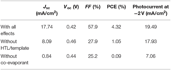
Table 1. Characteristic of the OPVs shown in Figure 7.
The actual area of each fabricated device was 1.21 (11 mm × 11 mm) or 0.09 cm2 (2 mm × 2 mm) and the active area under illumination was defined as 1.00 or 0.04 cm2, respectively, by a precision aperture mask positioned directly on the substrate side of the cell facing the incident light. The measured Jsc did not depend on the area of apertures or device dimensions (i.e., Isc always increased depending on them).
Structure Characterization
XRD and FESEM measurements were performed using a powder X-ray diffractometer RINT UltimaIII (Rigaku) and a field emission scanning electron microscope SU6600 (Hitachi High-Tech), respectively. Optical microscope images were analyzed using an optical microscope ECLIPSE LV100ND (Nikon) customized by Ozawa Science Co. Ltd., which is equipped with polarizer units, an apochromatic 150× objective lens CFI60-2 TU Plan Apo BD (Nikon), Piezo objective scanner PIFOC P-721.SDA (PI), color camera head units of DS-Fi2 and DS-U3 (Nikon), and measurement software Sensiv Measure (Mitani). The scale of the optical microscope was calibrated using an objective micrometer (Nikon).
Light Absorption Characterization and Calculation
The following Equations (1)–(5) were used to calculate the absorption spectrum of the active layer from the reflectance measurements of each actual device on ITO/FTO glass. Glass absorption, glass surface and glass/active layer interface reflections have been removed by the calculation. Equation (6) is also for the absorption spectrum of the active layer of the devices, however, which is based on the measurement results of the transmittance of each actual active layer on the ITO/FTO glass without the Ag electrode. Therefore, the effect of the standing wave caused by the Ag electrode is not included in Equation (6).
In order to accurately evaluate the optical properties, the absorption spectrum of the active layer inside the device was distinguished from the absorption of the active layer on the ITO/FTO glass substrate using measured transmittance (T) and reflectance (R) of these two samples in equations 1–6, where the subscripts indicate various specimens: glass: ITO/FTO glass substrate; glass & active: ITO/FTO glass substrate and the active layer (the device without the Ag anode and the anode buffer); glass & Ag: the ITO/FTO glass substrate on which Ag was deposited; device: the entire device including all layers.
Figure 1 shows the schematics of the specimens and the simplified light paths considered in these equations. Equations (1) and (2) extract the transmittance of the ITO/FTO glass substrate considering the incident light entering the glass, Tglass_incident, and the light reflected by the Ag anode, Tglass_reflection. From these values and Equations (3) and (4), two components of absorption by the ITO/FTO glass in the device can be calculated, Aglass_incident, absorption of the incident light, and Aglass_reflection, absorption of the light reflected by the Ag anode.
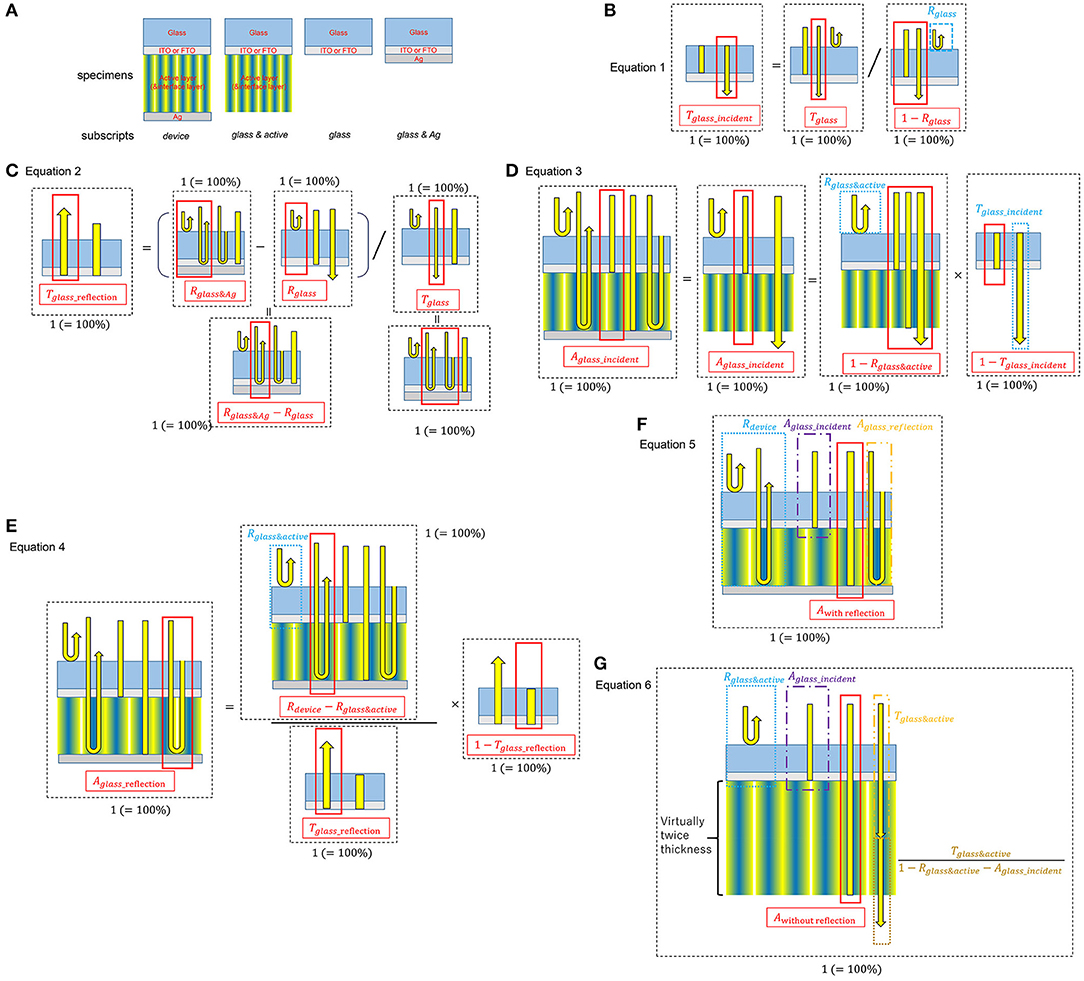
Figure 1. Schematics of optical absorption calculation from transmittance/reflectance measurements. (A) Schematics of the specimens for the measurements. (B–G) are schematics of Equations 1–6, respectively.
Consequently, subtraction of Aglass_incident, Aglass_reflection, and Rdevice yields the actual light absorption of the active layer inside the device, Awith reflection (Equation 5). In Equation (6), Awithout reflection is the absorption of the active layers without the effect of optical reflection at the Ag anode electrode, such as the standing waves. It is calculated from the square of transmittance of the active layers without the Ag anode.
To calculate the intensity of absorbed light under AM1.5G illumination, the photon density of AM 1.5G one sun spectra was multiplied by the absorption spectra, Awith reflection and Awithout reflection, respectively, and they were integrated with respect to the wavelengths ranging from 350 to 850 nm. These intensities, at each active layer thickness, were then normalized by the integral of the photon density of the sunlight alone at 350–850 nm, leading to the absorbed light intensity with/without reflection lines in Figure 5. The amplification factor is simply the ratio of the difference in the absorbed light intensity with/without reflection and the absorbed light intensity without reflection.
Results and Discussion
Thickness-Dependent Photovoltaic Properties
For this thickness-dependent OPV study, we selected ZnPc:C60, a standard donor:acceptor blend (Pfuetzner et al., 2009; Schueppel et al., 2010; Iketaki et al., 2011; Zhou et al., 2012; Lee et al., 2014; Wang et al., 2014; Holzmueller et al., 2015) of vacuum-deposited zinc phthalocyanine and fullerene pigments, as the active layer. The range of thicknesses for the active layer was 40–10,000 nm (Figure 2A). Thin interfacial layers, positioned above and below the active layer, were used to provide transfer and blocking of each charge carrier from the active layer and to serve as a template for the deposition of the active layer. They were also deposited by vacuum evaporation. The layer sequence, individual layer composition, and the thickness of the OPV cells fabricated in this study are as follows: [ITO/F4TCNQ (0.6 nm)/CuI (3 nm)/ZnPc (2 nm)/C60 (2.5 nm)/ZnPc (1 nm)/ZnPc:C60 (1.5:1 in volume ratio, 40–10,000 nm)/C60 (5 nm)/Alq3:C60 (1:1, 25 nm)/LiF (2 nm)/Ag (100/600/1,500 nm)], where ITO (indium tin oxide) is the transparent conductor, F4TCNQ is 2,3,5,6-tetrafluoro-7,7,8,8-tetracyanoquino-dimethane, and Alq3 is tris(8-quinolinolato)aluminum. To provide continuous coverage, the thickness of the vacuum-deposited Ag electrode was varied; 100, 600, and 1,500 nm for 40–1,000, 1,000–4,000, and 4,000–10,000 nm of ZnPc:C60, respectively.
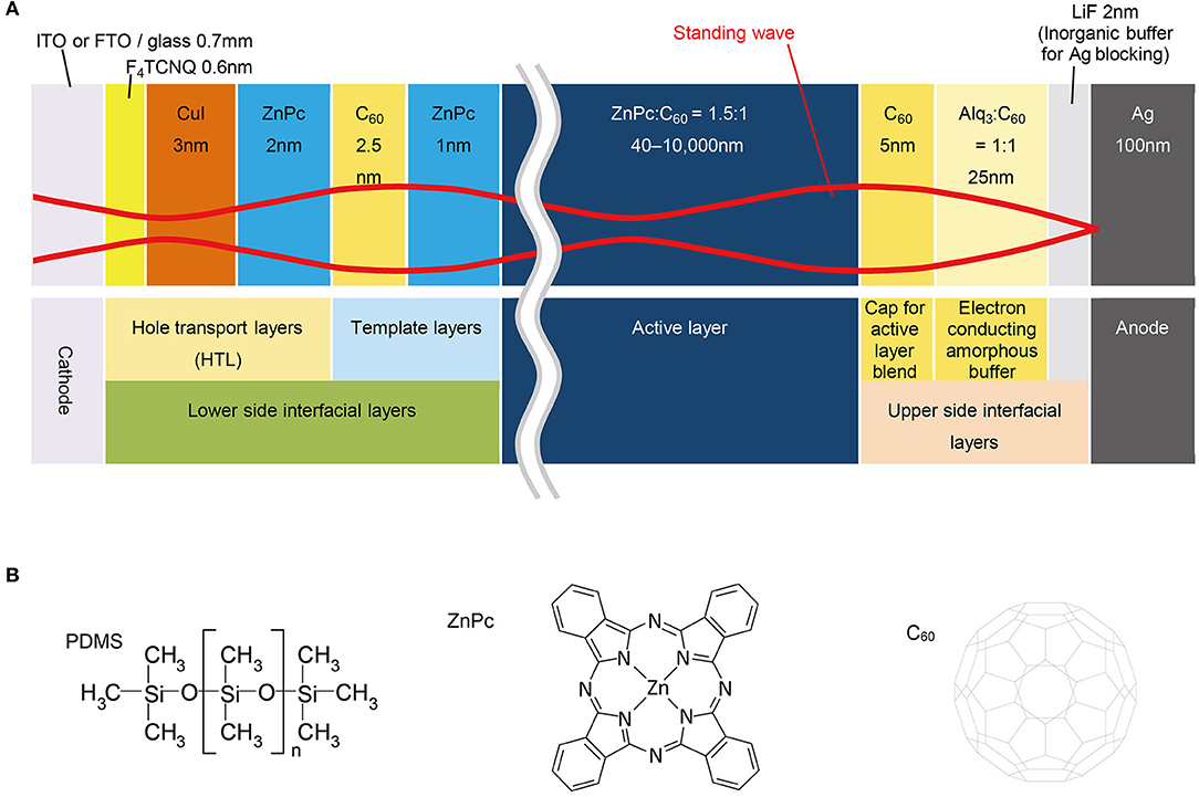
Figure 2. Device structure and materials. (A) Device structure of OPVs schematically drawn with the standing wave. (B) Chemical structures of co-evaporant (PDMS) and active layer materials used in this study.
For the deposition of ZnPc, C60, and ZnPc:C60 layers, we used a unique method of “co-evaporant induced crystallization (Kaji et al., 2011, 2013; Holzmueller et al., 2015)”, which enabled crystallization and growth control of a molecular film during vacuum evaporation. In this method, a liquid molecule was introduced as a co-evaporant during the evaporation of molecular films. The function of this liquid molecule was to induce crystallization of the deposited film. Because of its high volatility, it was removed from the film during film growth. The substrate was usually kept at an elevated temperature to facilitate the removal of the co-evaporant. Polydimethylsiloxane (PDMS, Figure 2B) was utilized as the co-evaporant and substrates were typically kept at 70°C during film growth. The other layers in the OPV cell were deposited without the co-evaporant and the substrates were held at 25°C. The experimental section in the “Materials and Methods” presents the conditions of depositions in detail. Figure 3 shows the thickness dependence of the OPV characteristics with and without a co-evaporant measured under one sun illumination of AM1.5G-simulated light and the difference is dramatic.
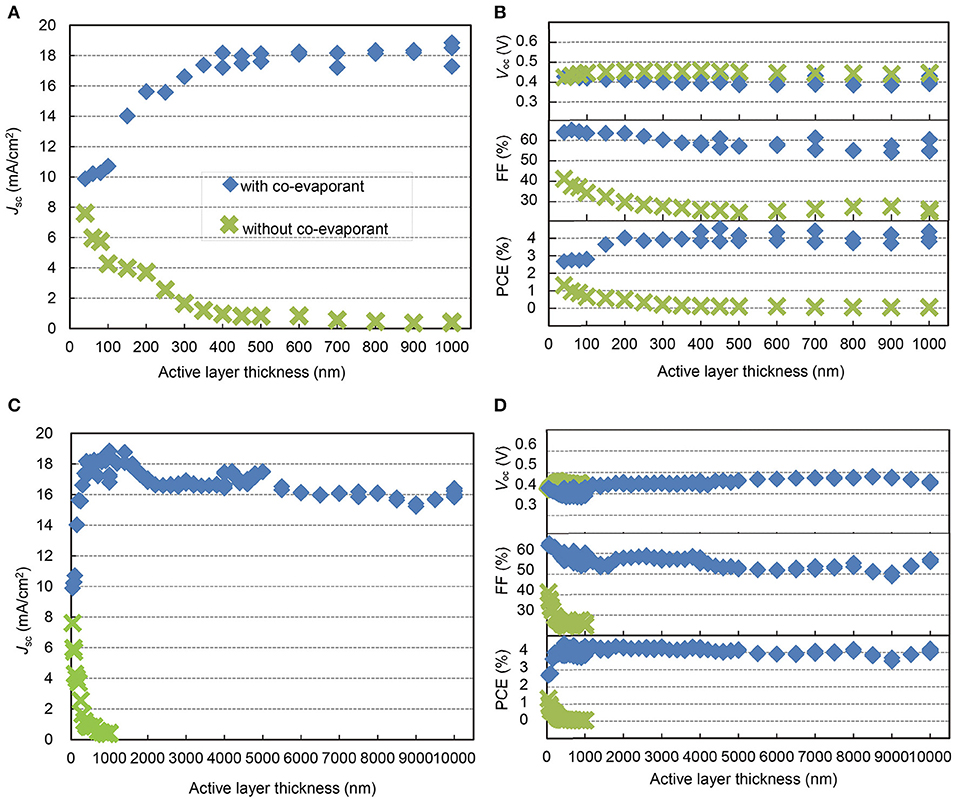
Figure 3. Thickness-dependent properties of ZnPc:C60 OPVs. Jsc, (A,C), Voc, FF, and PCE (B,D) of ZnPc:C60 OPVs with each active layer thickness to 1 μm (A,B) and 10 μm (C,D), with (blue square)/without (green cross) crystallization by the co-evaporant of PDMS.
Without induced crystallization by PDMS, the short-circuit current density, Jsc, of the OPV cells decreased dramatically toward <1 mA/cm2 as the blend ZnPc:C60 layer became thicker than 40 nm (Figure 3A) (Pfuetzner et al., 2009; Zhou et al., 2012). This is caused by an increase in geminate electron-hole recombination in the blend ZnPc:C60 layer as well as the loss of carriers in transit to the electrodes due to non-geminate recombination. Although these ZnPc:C60 blend layers were deposited at 70°C, this substrate heating by itself could not promote crystallization in the blend layer. With crystallization induced by evaporation with PDMS, Jsc is dramatically higher and increases with increasing active layer thickness, leveling off at about 18 mA/cm2 between 400 and 1,000 nm. The open-circuit voltage, Voc, shows little dependence on crystallization, varying between 0.40–0.45 V for the entire film thickness range (Figure 3B). The fill factor, FF, is highly dependent on crystallization. Without crystallization, FF decreases gradually as the blend film thickness increases, leveling at 25% for thicknesses above 400 nm. With crystallization, FF is only marginally dependent on the thickness of the blend film, peaking above 60% for thinner films and being maintained above 55% throughout the 400–1,000 nm range. As a result, the power conversion efficiency (PCE) for cells with crystallization is relatively constant at around 4.0%, independent of the thickness of the blend layer up to 1,000 nm.
In Figures 3C,D, the thickness dependence of the photovoltaic parameters is extended to 10 μm. Although relatively small decrease and upticks were found in both Jsc and FF, they are rather remarkable considering the extraordinary range of thicknesses. The Jsc levels are around 16 mA/cm2 at 2–10 μm compared to the maximum value of 18 mA/cm2 at 0.5–1.0 μm. Although FF appears to be more scattered (Figure 3D), in general, it shows only a gradual decrease and a slight uptick from 60 to 50% because of the surface roughness of thick ZnPc:C60 layers, which causes the top Ag electrode to be non-reflecting in appearance and possibly less electrically conductive. For this reason, it was necessary to use a thicker Ag layer (>1,500 nm) as the electrode for cells with thicker active layers (>4 μm). Figure 3D also shows the dependence of Voc on active layer thickness; Voc varies between 0.40 and 0.48 V over an extended range of thicknesses, for no apparent reason. The overall PCE retains a value of about 4.0% for all cells fabricated for this study. Clearly Figures 3C,D, demonstrate the most remarkable impact of using a co-evaporant for active layer deposition on OPV performance. Without a co-evaporant, the OPV cell is operational only with an active layer well below a micron. With a co-evaporant, it functions well even at 10 μm and possibly beyond.
Crystalline and Morphological Structures Induced by Co-evaporant
Figure 4 shows evidence of crystallization in the blend ZnPc:C60 films induced by a co-evaporant. Optical absorption and X-ray diffraction (XRD) were used to identify the difference between the films deposited with and without a co-evaporant. Comparing the absorption spectra (Figure 4A) and XRD patterns (Figure 4B), it is evident that absorption peaks (around 445 nm) and XRD peaks (10.3° and 10.8°) attributable to crystalline C60 clearly appear only in the film deposited with a co-evaporant. FWHM (full width at half maximum) of these peaks for 600-nm-thick ZnPc:C60 films were, 1.3° for FCC- C60(111) peak without co-evaporant but 0.2° with co-evaporant. HCP-C60(100) peak could not be found without co-evaporant but FWHM was 0.2° with co-evaporant.
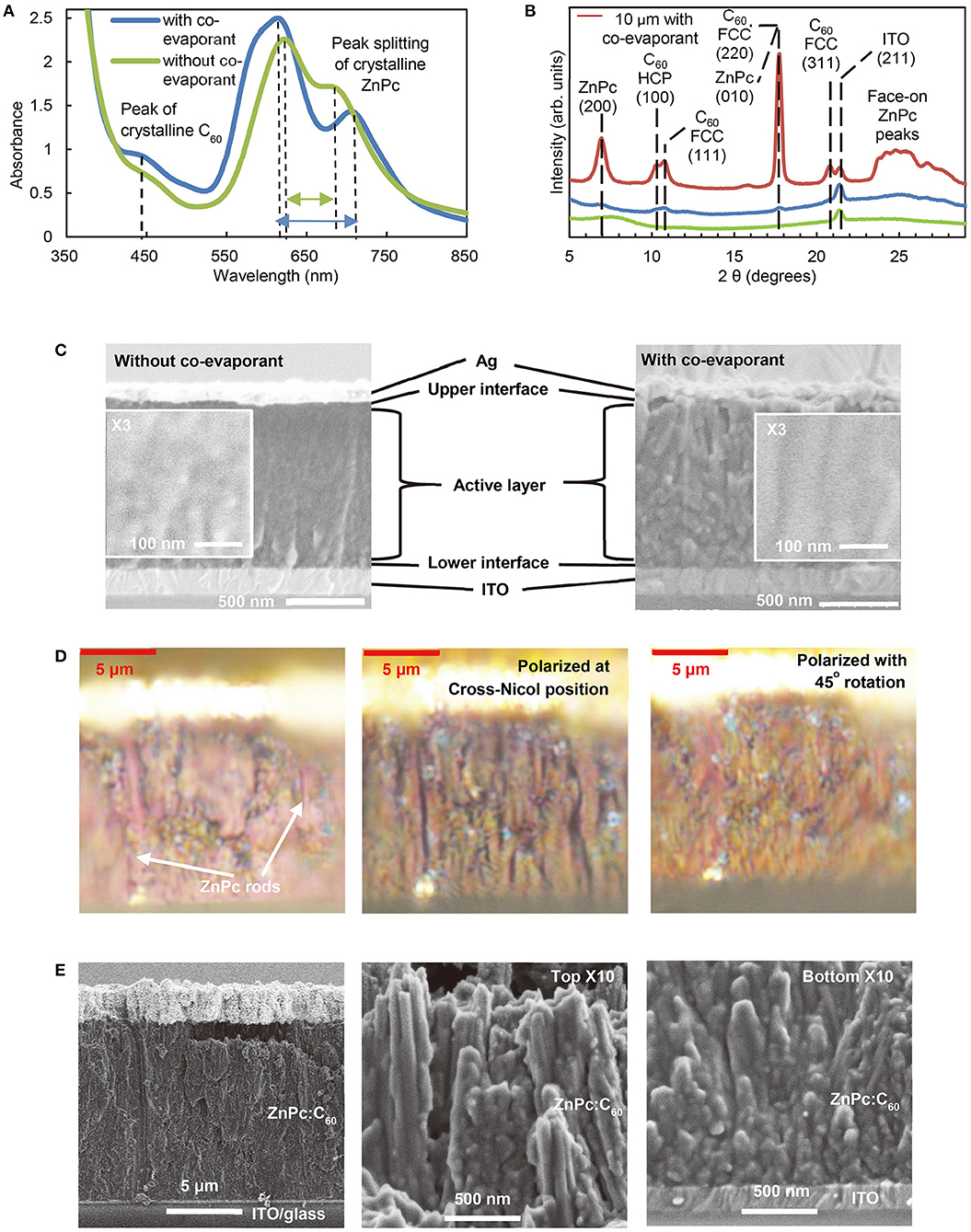
Figure 4. Effects of co-evaporant on ZnPc:C60 blend films. (A) UV-Vis-NIR absorbance spectra of 400 nm film converted from transmittance, (B) XRD patterns of 600 nm, and (C) Cross-sectional SEM images of 1,000 nm ZnPc:C60 with/without co-evaporant. Additionally, (B) includes the 10-μm-thick ZnPc:C60 cell with co-evaporant, whose cross-section was observed as the epi-illuminated optical microscope image and the polarized microscope images (D), and the SEM images (E).
For ZnPc, the absorption peaks show a wider split (620–710 nm) and the amorphous halo at the 7–10° range disappears in XRD. These changes in XRD patterns observed in our thick crystalline films were in agreement with what has been previously reported for thin (100 nm) ZnPc:C60 films (Holzmueller et al., 2015). FWHM of the ZnPc(200) peak was 0.7° with co-evaporant, whereas this peak could not be found without co-evaporant. The XRD peaks for the 10 μm film (red line in Figure 4B) are very sharp and strong but the FWHM of these peaks were almost same as them of 600-nm-thick films. No preferred orientations are indicated for ZnPc and C60. The orientation indices identified in Figure 4B were obtained from the literature (Cheng et al., 2010; Iketaki et al., 2011; Kaji et al., 2011; Zhou et al., 2012; Lee et al., 2014; Holzmueller et al., 2015).
Figure 4C presents the comparison of the morphology of 1-μm ZnPc:C60 films deposited with/without a co-evaporant as observed by scanning electron microscope (SEM). The cross-sectional images show that the control film without a co-evaporant is composed of randomly oriented grains, whereas column-like structures are visible in the film deposited with a co-evaporant. This difference in morphological structures has been reported for the H2Pc:C60 film in our previous studies (Kaji et al., 2011, 2013). Our present study on ultra-thick films further reveals that major morphological changes are caused by the crystallization of the ZnPc component in ZnPc:C60 blend films.
Figure 4D shows the optical microscope images of a 10-μm ZnPc:C60 film. The left cross-sectional image is an optical microscope image with usual epi-illumination from above, where rod-shaped domains (purple-red color) can be found in the vertical direction (perpendicular to the substrate plane). These rods can be identified as ZnPc crystals, compared to the bulk shape and the color of common ZnPc needle single crystals, while the grains surrounding the rods can be attributed to the C60 crystals. With polarizers, these rods were more clearly observed as black shadow stripes for the center image taken at the cross-Nicol position, whereas this color extinction was canceled for the right image taken when the position of polarizers were rotated by 45°. These polarized images confirm the existence of highly crystalline ZnPc rods over the ZnPc:C60 active layer.
Figure 4E shows the SEM images of the same 10-μm-thick film (the actual value was 12 μm, according to both optical and SEM images). The left image shows the same area as Figure 4D. The center and right images show, respectively, the top and the bottom (adjacent to substrate) of the film at higher magnification. The rods are about 100 nm in diameter, surrounded by multiple outer domains of similar size. The rods at the top are more vertical and more solid than the ones at the bottom near the ITO substrate. Thus, both SEM and optical microscope observations indicate that the ZnPc:C60 blend film produced with a co-evaporant is highly crystalline and consists of rod-shaped ZnPc domains surrounded by crystalline C60 grains. Since these rod and grain shape of crystals are similar to the shape of their bulk crystals, it is suggested that other pigments having a needle-like or plate-like crystal form in bulk might achieve similar characteristics of ultra-thick films as ZnPc:C60 system in future.
Correspondence Between Thickness-Dependent Photovoltaic and Optical Properties
Light absorption by the active layer in an OPV cell depends on several factors including the layer thickness, reflectance of the top Ag electrode, and the roughness of the ITO substrate. In Figures 5A,B, the total amount of light absorbed by the active layer is plotted against the layer thickness for two different substrates, flat ITO glass and textured F-doped tin oxide (FTO) glass, respectively. In other words, this intensity corresponds to the thickness dependent optical efficiency of the photovoltaic cells to the standard sun light spectrum at 350–850 nm range, if we can ignore the optical loss for the optical aperture and electrical contacts for precise measurement because these cells were not the modules cells for practical use and thus the definition of optical efficiency could be different.
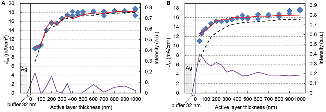
Figure 5. Correspondence of photocurrent and absorbed light intensity. Jsc (blue square, referring to left axis) at each ZnPc:C60 thickness on flat ITO substrate (A), and textured FTO substrate (B), corresponding to the normalized intensity of absorbed light with/without reflection at Ag anode (red solid/black broken lines, referring to right axes), calculated from reflectance of actual devices and the square of transmittance of the same active layers, respectively. The amplification rate between the absorbed light intensities with/without reflection is also indicated (purple lines).
Also plotted in these two figures are the short-circuit currents from the corresponding OPV cells. The light absorption by the active layers was based on AM1.5G illumination and calculated with and without the top Ag electrode. Respectively, they were calculated from the measured reflectance of actual OPV cells with Ag (red lines in Figures 5A,B) and from the square of the measured transmittance of the same active layers used in the OPV cells but without Ag (dotted lines). The calculated absorption intensities were integrated over the spectral range of 350–850 nm and normalized with respect to one sun of AM1.5G. Additionally, we calculated the amplification factor, which is the ratio of the difference in the absorbed light intensity with/without the reflection and the intensity of the absorbed light without Ag. The “Materials and Methods” section presents the details of the calculations. Although the absorbed light intensity without Ag reflection gradually increases with the active film thickness, both plots of Jsc and absorbed light intensity with Ag reflection indicate wavy curves with local maxima, which is evident at thicknesses below 400 nm. This is the effect of the standing waves, which have been utilized to optimize the OPV performance in previous reports (Maennig et al., 2004; Xue et al., 2004; Schueppel et al., 2010; Osaka et al., 2014; Jung et al., 2015).
The effect of standing waves in our OPV cells was evident at 40, 200, and 350 nm, corresponding to the antinodes of the first, second, and third standing waves, respectively (Figure 5A). These standing wave features appear in photocurrent and light intensity plots. The photocurrent continues to increase up to the node of the third standing wave (400 nm) and becomes nearly saturated up to 1,000 nm. The correlation between Jsc and the absorbed light intensity is very strong. To confirm this correlation, we should notify that we did not simulate the standing waves by calculation but read from the results of optical absorption spectra from transmittance/reflectance measurements of actual devices.
Additionally, we examined the OPV cells fabricated on a textured substrate, which is intended to increase the optical path-length through the active layer due to light scattering (Müller-Meskamp et al., 2012). Instead of flat ITO glass, which has a low average maximum height of surface roughness Rz < 1 nm, we used textured FTO glass as the substrate with a much higher surface roughness, Rz > 100 nm. Figure 5B shows that the textured FTO glass is more effective than the standing waves in enhancing the light absorption of thin active layers (below 300 nm). Nevertheless, higher photocurrent is obtained above 400 nm, where the texture effect is small. This indicates that the optical and texture effects only minimally affect photocurrent generation in thick OPV cells, as long as carrier recombination and transport through the active layer are not critical issues.
Figure 6 shows the reflectance depending on the thickness of active layer. Wavelength of 450, 550, 620, and 850 nm correspond to C60 peak, ZnPc:C60 valley, ZnPc peak and ZnPc absorption edge, respectively. Rdevice is the reflectance of the actual devices, and Rglass&active is it of specimens without Ag electrode mirror. In any specimens and wavelength, on flat or textured substrates, it was confirmed that the reflectance becomes smaller depending on the increase of the active layer thickness, when the effect of interference can be ignored. Judging from the difference between flat ITO and textured FTO, rough surfaces of textured FTO rather suppress the influence of interference on the reflectance, as well as on the light absorption plots in Figure 5.
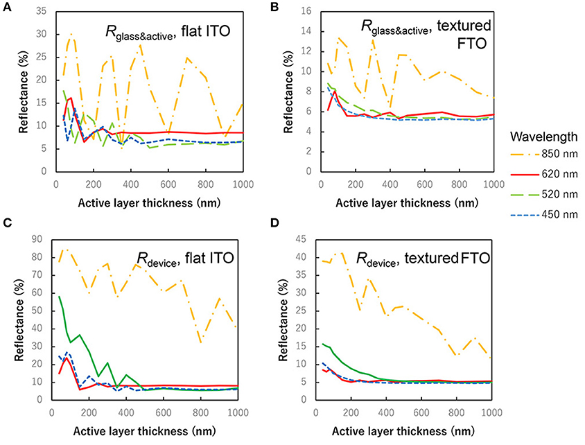
Figure 6. Thickness dependence of reflectance. (A) Rglass&active, reflectance of the device on flat ITO without Ag electrode. (B) Rglass&active, reflectance of the device on textured FTO without Ag electrode. (C) Rdevice, reflectance of the device on textured ITO covered with Ag electrode mirror. (D) Rdevice, reflectance of the device on textured FTO with Ag electrode mirror.
Comparison of Effects of Interfacial Layers and Crystallization
Last, Figure 2A shows the upper and lower interfacial layers designed to enhance the performance and reproducibility of OPV cells. For the upper interfacial layers, we used LiF (2 nm) directly below the Ag electrode to suppress the penetration of Ag into the active layer. In addition, we used Alq3:C60 (25 nm) as a buffer underneath the LiF layer. This Alq3:C60 buffer, although relatively thin, is effective in further shielding the donor material in the active layer from the Ag electrode. Although the C60 (5 nm) layer below this buffer forms a donor/acceptor contact, it is not sufficient to terminate the donor:acceptor blend because it tends to form a large grain boundary, which would be induced by the high crystalline nature of the present active layer. In contrast, the Alq3:C60 buffer has both a conformal and amorphous (Mori and Masumoto, 2006) nature to cover the interface, which can be easily confirmed by optical microscope observations and UV-Vis absorption, respectively. Owing to these properties and the somewhat conductive (Kao et al., 2009; Bartynski et al., 2013) nature, this buffer layer is useful over wide active layer thicknesses. When these upper interface layers are totally removed, the OPV cells rarely work and often indicate unstable leak currents. For the lower interface, a sequence of layers consisting of F4TCNQ (0.6 nm)/CuI (3 nm)/ZnPc (2 nm)/C60 (2.5 nm)/ZnPc (1 nm) was used. The F4TCNQ/CuI/ZnPc layers directly above the ITO electrode served as the hole-transfer layer to improve the anode contact (Cheng et al., 2010; Zhou et al., 2012). The C60/ZnPc layers served as the template layer to reproduce the starting block of the growth of the active ZnPc:C60 blend layer. The cells with all these injection layers exhibited good thermal stability during the two heating/cooling cycles, 100°C for 1 h and cooling to 25°C without bias. They showed no degradation in J-V characteristics.
In order to quantitatively distinguish the effects of these layers from those of crystallization induced by the co-evaporant, we fabricated a set of OPV cells with common 600-nm-thick ZnPc:C60 active layers with and without the lower interfacial layers. The J-V characteristics and the incident photon to current efficiency (IPCE) spectra of these cells are compared in Figures 7A,B and Table 1. Crystallization by the co-evaporant has the greatest impact on Jsc, while the bottom interfacial layer is needed to significantly improve Jsc as well as FF.
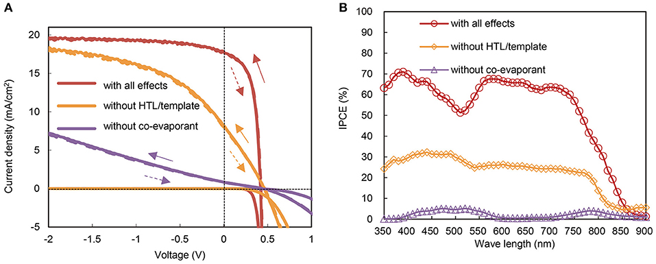
Figure 7. Various effects on photocurrent of OPVs with over-400-nm-thick active layers. (A) Current density–voltage (J-V) characteristics of 600-nm-thick ZnPc:C60 devices with/without effects of lower interfacial layers and crystallization by co-evaporant. Components are with all effects (red), without hole-transfer layer (HTL) and template layer (orange), and without crystallization (purple), respectively. The solid/broken style indicates the voltage sweep direction. (B) IPCE spectra of the same set of the cells. Measurement area is 1.0 cm2 for J-V curves and 0.04 cm2 for IPCE.
In addition to the large differences of OPV characteristics in Tables 1, 2 shows large difference of series resistance (Rs) and accompanying difference of shunt resistance (Rsh). This large difference of Rs between “with all effects” and “without co-evaporant” can be attributed to the carrier transport in the active layer, whereas the difference between “with all effects” and “without co-evaporant” can be attributed mainly to the carrier transport at HTL. These difference of carrier transport also resulted in the large difference of Jsc and FF in Table 1. This difference between “with all effects” and “without co-evaporant” can be also noticeable in Figure 7B, where the shape of IPCE spectrum of the former device corresponds to the optical absorption spectra in Figure 4A but the spectrum shape of the latter device is opposite at 550–800 nm range. This filter effect can also be attributed to bad transport of carriers, especially, of electrons.
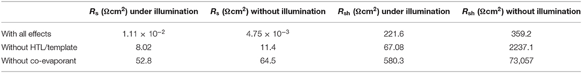
Table 2. Resistances of the OPVs shown in Figure 7.
Conclusion
We demonstrated that efficient OPV cells can be produced using an extraordinarily thick crystalline ZnPc:C60 film as the active layer along with the adjacent interfacial layers for further performance enhancement. The power conversion efficiency of about 4% and short-circuit density as high as 16 mA/cm2 were achieved with an active layer as thick as 10 μm, which is well beyond what is commonly needed for optical optimization. The crystalline ZnPc:C60 film was produced by vacuum deposition with a co-evaporant. These results proved that crystalline pigment layer with a thickness much greater than what is needed for optical optimization can be utilized for organic optoelectronic devices and that organic optoelectronic devices have potentiality to relief their design from co-optimization of optics and charge transport.
Data Availability Statement
The datasets generated for this study are available on request to the corresponding author.
Author Contributions
MK and TK are the main contributors to this work. SN performed the FESEM analyses. TK and MH guided the work. All authors discussed the results and commented on the manuscript.
Funding
This study has been mainly conducted in Tokyo University of Agriculture and Technology, supported in part by Advanced Low Carbon Technology Research and Development Program (ALCA) of Japan Science and Technology Agency (JST), JSPS KAKENHI Grant Number 17H04807, and by Nanotechnology Platform Program (Molecule and Material Synthesis) of the Ministry of Education, Culture, Sports, Science and Technology (MEXT), Japan.
Conflict of Interest
The authors declare that the research was conducted in the absence of any commercial or financial relationships that could be construed as a potential conflict of interest.
Acknowledgments
We thank Prof. C. W. Tang and Dr. S. Dong from Hong Kong University of Science and Technology for discussions and suggestions.
References
Bartynski, A. N., Trinh, C., Panda, A., Bergemann, K., Lassiter, B. E., Zimmerman, J. D., et al. (2013). A fullerene-based organic exciton blocking layer with high electron conductivity. Nano Lett. 13, 3315–3320. doi: 10.1021/nl401531t
Cheng, C. H., Wang, J., Du, G. T., Shi, S. H., Du, Z. J., Fan, Z. Q., et al. (2010). Organic solar cells with remarkable enhanced efficiency by using a CuI buffer to control the molecular orientation and modify the anode. Appl. Phys. Lett. 97:083305. doi: 10.1063/1.3483159
Dou, L., You, J., Hong, Z., Xu, Z., Li, G., Street, R. A., et al. (2013). 25th anniversary article: a decade of organic/polymeric photovoltaic research. Adv. Mater. 25, 6642–6671. doi: 10.1002/adma.201302563
Holzmueller, F., Wilde, L., Wölzl, F., Koerner, C., Vandewal, K., and Leo, K. (2015). Co-evaporant induced crystallization of zinc phthalocyanine:C60 blends for solar cells, Org. Electron. 27, 133–136. doi: 10.1016/j.orgel.2015.08.031
Iketaki, K., Kaji, T., Nakao, S., and Hiramoto, M. (2011). Structural studies of the co-deposited i-layer of ZnPc:C60 p-i-n solar cells M., Phys. Status Solidi C 8, 637–639. doi: 10.1002/pssc.201000462
Jin, Y., Chen, Z., Dong, S., Zheng, N., Ying, L., X.-Jiang, F., et al. (2016). A novel Naphtho[1,2-c:5,6-c′]Bis([1,2,5]Thiadiazole)-based narrow-bandgap π-conjugated polymer with powerconversion efficiency over 10%. Adv. Mater. 28, 9811–9818. doi: 10.1002/adma.201603178
Jung, J. W., Russell, T. P., and Jo, W. H. (2015). Highly crystalline low band gap polymer based on Thieno[3,4-c]pyrrole-4,6-dione for high-performance polymer solar cells with a >400 nm thick active layer. ACS Appl. Mater. Interfaces 7, 13666–13674. doi: 10.1021/acsami.5b03446
Kaji, T., Nakao, S., and Hiramoto, M. (2013). Effect of co-evaporant induced crystallization on needle growth of phthalocyanine thin films. Mol. Cryst. Liq. Cryst. 578, 63–67. doi: 10.1080/15421406.2013.804376
Kaji, T., Zhang, M., Nakao, S., Iketaki, K., Yokoyama, K., Tang, C. W., et al. (2011). Co-evaporant induced crystalline donor: acceptor blends in organic solar cells. Adv. Mater. 23, 3320–3325. doi: 10.1002/adma.201101305
Kang, H., Kim, G., Kim, J., Kwon, S., and Kim, H. (2016). Bulk-heterojunction organic solar cells: five core technologies for their commercialization. Adv. Mater. 28, 7821–7861. doi: 10.1002/adma.201601197
Kao, P.-C., Chu, S.-Y., Huang, H.-H., Tseng, Z.-L., and Chen, Y.-C. (2009). Improved efficiency of organic photovoltaic cells using tris (8-hydroxy-quinoline) aluminum as a doping material. Thin Solid Films 517, 5301–5304. doi: 10.1016/j.tsf.2009.03.147
Ko, S.-J., Walker, B., Nguyen, T. L., Choi, H., Seifter, J., Uddin, M. A., et al. (2016). Photocurrent extraction efficiency near unity in a thick polymer bulk heterojunction. Adv. Funct. Mater. 26, 3324–3330. doi: 10.1002/adfm.201505556
Lee, J., Park, D., Heo, I., and Yim, S. (2014). Effect of cuprous halide interlayers on the device performance of ZnPc/C60 organic solar cells. Mater. Res. Bull. 58, 132–135. doi: 10.1016/j.materresbull.2014.03.030
Luo, G., Ren, X., Zhang, S., Wu, H., Choy, W. C. H., He, Z., et al. (2016). Recent advances in organic photovoltaics: device structure and optical engineering optimization on the nanoscale. Small 12, 1547–1571. doi: 10.1002/smll.201502775
Maennig, B., Drechsel, J., Gebeyehu, D., Simon, P., Kozlowski, F., Werner, A., et al. (2004). Organic p-i-n solar cells. Appl. Phys. A 79, 1–14. doi: 10.1007/s00339-003-2494-9
Meng, L., Zhang, Y., Wan, X., Li, C., Zhang, X., Wang, Y., et al. (2018). Organic and solution-processed tandem solar cells with 17.3% efficiency. Science 361, 1094–1098. doi: 10.1126/science.aat2612
Mishra, A., and Bäuerle, P. (2012). Small molecule organic semiconductors on the move: promises for future solar energy technology. Angew. Chem. Int. Ed. 51, 2020–2067. doi: 10.1002/anie.201102326
Mori, T., and Masumoto, Y. (2006). Effect of organic alloy for suppression of polycrystallization in BCP thin film. J. Photopolym. Sci. Tech. 19, 209–214. doi: 10.2494/photopolymer.19.209
Müller-Meskamp, L., Kim, H. Y., Roch, T., Hofmann, S., Scholz, R., Eckardt, S., et al. (2012). Efficiency enhancement of organic solar cells by fabricating periodic surface textures using direct laser interference patterning. Adv. Mater. 24, 906–910. doi: 10.1002/adma.201104331
Osaka, I., Saito, M., Koganezawa, T., and Takimiya, K. (2014). Thiophene–thiazolothiazole copolymers: significant impact of side chain composition on backbone orientation and solar cell performances. Adv. Mater. 26, 331–338. doi: 10.1002/adma.201303059
Pfuetzner, S., Meiss, J., Petrich, A., Riede, M., and Leo, K. (2009). Thick C60:ZnPc bulk heterojunction solar cells with improved performance by film deposition on heated substrates. App. Phys. Lett. 94:253303. doi: 10.1063/1.3154554
Price, S. C., Stuart, A. C., Yang, L., Zhou, H., and You, W. (2011). Fluorine substituted conjugated polymer of medium band gap yields 7% efficiency in polymer-fullerene Solar cells. J. Am. Chem. Soc. 133, 4625–4631. doi: 10.1021/ja1112595
Riede, M., Uhrich, C., Widmer, J., Timmreck, R., Wynands, D., Schwartz, G., et al. (2011). Efficient organic tandem solar cells based on small molecules. Adv. Funct. Mater. 21, 3019–3028. doi: 10.1002/adfm.201002760
Roncali, J., Leriche, P., and Blanchard, P. (2014). Molecular materials for organic photovoltaics: small is beautiful. Adv. Mater. 26, 3821–3838. doi: 10.1002/adma.201305999
Sakai, K., and Hiramoto, M. (2008). Efficient organic p-i-n solar cells having very thick co-deposited i-Layer consisting of highly purified organic semiconductors. Mol. Cryst. Liq. Cryst. 491, 284–289. doi: 10.1080/15421400802330960
Schueppel, R., Timmreck, R., Allinger, A., Mueller, T., Furno, M., Uhrich, C., et al. (2010). Controlled current matching in small molecule organic tandem solar cells using doped spacer layers. J. Appl. Phys. 107:044503. doi: 10.1063/1.3277051
Søndergaard, R., Hösel, M., Angmo, D., Larsen-Olsen, T. T., and Krebs, F. C. (2012). Roll-to-roll fabrication of polymer solar cells. Mater. Today 15, 1–2. doi: 10.1016/S1369-7021(12)70019-6
Song, B., Rolin, C., Zimmerman, J. D., and Forrest, S. R. (2014). Effect of Mixed layer crystallinity on the performance of mixed heterojunction organic photovoltaic cells. Adv. Mater. 26, 2914–2918. doi: 10.1002/adma.201305099
Wang, Z., Miyadera, T., Yamanari, T., and Yoshida, Y. (2014). Templating effects in molecular growth of blended films for efficient small-molecule photovoltaics. ACS Appl. Mater. Interfaces 6, 6369–6377. doi: 10.1021/am405740c
Xue, J., Rand, B. P., Uchida, S., and Forrest, S. R. (2005). A hybrid planar–mixed molecular heterojunction photovoltaic cell. Adv. Mater. 17, 66–71. doi: 10.1002/adma.200400617
Xue, J., Uchida, S., Rand, B. P., and Forrest, S. R. (2004). Asymmetric tandem organic photovoltaic cells with hybrid planar-mixed molecular heterojunctions. Appl. Phys. Lett. 85, 5757–5759. doi: 10.1063/1.1829776
Keywords: pigment, crystallization, organic electronics, organic photovoltaics, solar cell, bulk hetero-junction
Citation: Katayama M, Kaji T, Nakao S and Hiramoto M (2020) Ultra-Thick Organic Pigment Layer Up to 10 μm Activated by Crystallization in Organic Photovoltaic Cells. Front. Energy Res. 8:4. doi: 10.3389/fenrg.2020.00004
Received: 30 June 2019; Accepted: 09 January 2020;
Published: 28 January 2020.
Edited by:
Itaru Osaka, Hiroshima University, JapanCopyright © 2020 Katayama, Kaji, Nakao and Hiramoto. This is an open-access article distributed under the terms of the Creative Commons Attribution License (CC BY). The use, distribution or reproduction in other forums is permitted, provided the original author(s) and the copyright owner(s) are credited and that the original publication in this journal is cited, in accordance with accepted academic practice. No use, distribution or reproduction is permitted which does not comply with these terms.
*Correspondence: Toshihiko Kaji, a2FqaS10QGNjLnR1YXQuYWMuanA=