 Weiru Wang
 Limeng Wang1*
- 1Key Laboratory of Modern Power System Simulation and Control and Renewable Energy Technology, Ministry of Education (Northeast Electric Power University), Jilin, China
- 2EHV Power Transmission Company Guangzhou Branch, China Southern Power Grid, Guangzhou, China
In order to fully study the working characteristics of large-scale power electronic devices in the field of renewable energy delivery, it is imperative to build digital and physical hybrid simulation platforms. A power interface algorithm based on damping impedance is proposed to improve the stability of DC power grid hybrid platforms. Firstly, according to the characteristics of the open-loop transfer function of the damping impedance method, the matching principle between damping impedance at the power interface and equivalent impedance of the physical simulation system is obtained. Secondly, the calculation method of the equivalent impedance of multi-type equipment on the physical side is proposed, and the impedance real-time matching under different working conditions is realized. In order to reduce the simulation error caused by interface delay, a DC voltage interface delay compensation method based on slope prediction is proposed, and a prediction compensation model is established. A digital and physical hybrid platform for a four-terminal flexible DC power grid with DC circuit breakers is built to verify the proposed interface algorithm. The simulation results show that the proposed interface algorithm can effectively compensate for the interface delay and ensure the stable operation of the platform under different conditions.
Introduction
Vigorously developing renewable energy is an important means to realize the transformation of energy to clean and low carbon (Jiang et al., 2020). The flexible DC transmission technology based on modular multilevel converters (MMCs) has become an important way of renewable energy export with its advantages of a small harmonic component of output voltage and a current, low loss, and easy expansion (Akagi, 2011; Teeuwsen, 2011). For China's power system, with the continuous growth of the inland renewable energy power generation, the focus of DC construction has gradually shifted from coastal areas to inland areas; transmission lines have gradually changed from submarine cables to overhead lines; and the main wiring has gradually changed from point to point to the DC power grid (Wang et al., 2019; He et al., 2020). However, the overhead line is greatly affected by the natural environment, which makes the fault rate higher. Furthermore, DC power grid faults will have an impact on a wide area. Therefore, DC circuit breakers (DCCBs), fault current limiters (FCLs), or other fault current suppression equipment must be configured in the DC power grid to reduce the impact of a fault (Li et al., 2020; Wang et al., 2020).
In order to realize the accurate modeling and engineering parameter verification of the high-voltage flexible DC transmission network with fault current suppression equipment, it is necessary to use physical hardware equipment for experimental simulation (Matar et al., 2016). However, considering the limitations of the laboratory area and construction cost, it is difficult to build a complete physical flexible DC transmission platform (Kotsampopoulos et al., 2015). The digital and physical hybrid simulation technology [also known as “power hardware in the loop (PHIL)] is an effective means to solve the above difficulties, which means the hybrid platform combines the advantages of digital simulation and physical experiments. The operator can observe the physical equipment characteristics and the DC power grid dynamic characteristics by placing the key research objects in the physical sub-platform. Therefore, PHIL is an effective method for the simulation experiment of the flexible DC power grid with fault current suppression equipment.
The digital simulation system (DSS) and physical simulation system (PSS) of the PHIL platform are connected by A/D converters, D/A converters, and power amplifiers (PA) This link inevitably produces a time delay and introduces some disturbances, which will make the hybrid simulation platform instability. And after the system fault, the analysis of the cause of the fault current suppression equipment action, such as overcurrent or interface instability, will be impossible. At present, based on the findings of the past studies, several interface algorithms are proposed to improve the interface stability and the ideal transformer model (ITM); among them is the most traditional algorithm used for PHIL simulations even though its stability is weak (Steurer et al., 2010; Dargahi and Ghosh, 2014). Transmission line model is suitable for the DC system (Hu et al., 2012), but it needs decoupling elements to improve simulation performance. If transmission line model is used to simulate the DC power grid, the entire system would be complex. Damping impedance method (DIM) can match the real-time impedance of the DSS and PSS subsystems in real time, ensuring the simplicity of the algorithm and improving the stability and accuracy of the platform (Ren et al., 2008). According to measured voltage and current value, real-time impedance matching of DIM can be realized, but this method is only applicable to passive physical systems with fixed frequency (Paran et al., 2014).
In order to solve the above problems, an improved DIM algorithm for the flexible DC power grid with fault current suppression equipment is proposed in this paper. The innovation points are as follows:
(a) The sub-module (SM), converter, and fault current suppression equipment are equivalent based on the Thevenin theorem, and the dynamic impedance matching method is proposed according to the direction of the current flow in the power interface.
(b) The frequency of the DC fluctuation is monitored in real time to enable the accurate calculation of the equivalent reactance of the inductance at the DC interface.
(c) An interface delay compensation method based on the slope prediction strategy is proposed to improve the waveform fitting of the DSS and PSS subsystems.
(d) A two-terminal MMC digital simulation system, running in RT-LAB in real time, is built, using MATLAB. This DSS system, together with a two-terminal MMC physical platform and a DCCB physical platform, forms the PHIL platform to enable the verification of the stability and accuracy of the proposed algorithm.
Analysis of the DC Power Grid Phil Platform Structure and the DIM Interface Algorithm
Structure of the DC Power Grid PHIL Platform
Taking the four-terminal flexible DC power grid PHIL simulation platform as an example, the structure diagram is shown as Figure 1.
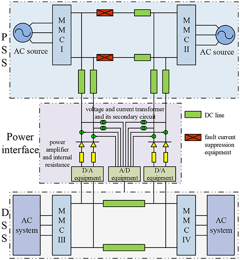
Figure 1. Four-terminal HVDC PHIL system structure.
The PSS subsystem is the key research object of the PHIL platform, which mainly includes MMC converters, arm reactors, converter transformers, AC/DC equivalent lines, various types of controllers and fault current suppression equipment required by the DC power grid, etc., for the dynamic physical simulation of the flexible DC network.
The working states of the AC/DC system are macro analyzed at the DSS subsystem that mainly includes MMC stations and an equivalent AC circuit. After being built by MATLAB software, it runs in RT-LAB and completes signal acquisition, calculation, output, and other tasks within the set simulation step size.
The power interface, which is responsible for the transmission and exchange of energy and signal between the DSS and PSS subsystems, mainly includes the interface algorithm and interface hardware devices. In this paper, the DIM interface algorithm is used at the PHIL platform, and the damping impedance is matched in real time. The interface hardware includes D/A converters, A/D converters, power amplifiers, Hall current and voltage sensors, etc. The digital signals of the DSS subsystem are converted by the D/A converters into analog signals, which are fed to the PSS subsystem through PA. The analog signals of the PSS subsystem collected by the Hall sensors transformers are converted by the A/D converters into digital signals, which are used in the next step for system parameter calculation and damping impedance matching by feeding them back to the DSS subsystem.
Analysis of the DIM Interface Algorithm
The DIM interface algorithm adds damping impedance Z* on the basis of the traditional ITM algorithm for the PHIL platform to have higher stability and accuracy. The schematic diagram of the algorithm is shown in Figure 2. In the figure, ZSH is the equivalent output impedance of PA. The equivalent DC power voltage US and equivalent impedance ZS constitute the equivalent circuit on the digital side. The equivalent DC power voltage UH and equivalent impedance ZH constitute the equivalent circuit on the physical side.
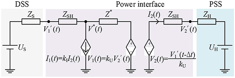
Figure 2. A schematic diagram of the DIM.
According to the transmission capacity and the voltage level of the DC systems at digital and physical sides, the proportional coefficients of the controlled voltage source and the controlled current source are calculated, using the following equations:
where UDSS and UPSS are the DC-rated voltages of digital and physical sides, respectively; PDSS and PPSS are the rated transmission powers of the DC system at the digital and physical sides, respectively.
According to Figure 2, the open-loop transfer function of the DIM algorithm for the DC power interface can be deduced as follows:
The DSS subsystem is affected by disturbances and an interface delay, and the errors of all simulation steps get accumulated, making the PHIL system unstable. According to the Nyquist stability criterion, in order to ensure that the platform is in the absolute stable state, the damping impedance Z* has to be matched with the ZH of the PSS subsystem at different working states in real time so that Z* becomes equal to (kU/kI)ZH and eliminates the accumulated errors.
DIM Impedance Matching
MMC Operation Mechanism and Equivalent Impedance Calculation
The valve-based controller of the MMC determines the input amount of each arm SM according to the arm voltage reference wave transmitted by the station-based controller, which means that the sinusoidal voltage waveform at AC port of MMC is fitted in the form of the step wave. So, when the MMC transmits power, each SM can be equivalent to a controllable voltage source.
The main circuit topology of the MMC converter, which has six arms, is shown in Figure 3. Each arm contains N number of SMs and arm inductance L, while each sub-module is composed of capacitance (C), two insulated gate bipolar transistors (IGBTs) (T1 and T2) and two reverse parallel diodes (D1 and D2).
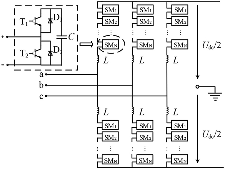
Figure 3. Main circuit of the MMC topology structure.
As can be seen from Figure 3, the resistance of each SM depends on its insert or bypass state. The on-state resistance of the IGBT and diode is RTon and RDon, respectively. Since the off-state resistance of the IGBT and diode is more than eight orders of magnitude larger than their respective on-state resistance, it can be considered that the off-state resistance is infinite. Depending on the direction of the current flow in the sub-module, the resistance RSM of each SM can be expressed as given below (Gnanarathna et al., 2011):
where S is the SM switch function (S = 1 when the SM is at the insert state and S = 0 when it is at the bypass state), RC is the equivalent resistance of capacitance, and Δt is the simulation step size.
In each simulation step, the number of insert-state SMs and bypass-state SMs is fed back by the valve-based controller to the DSS subsystem in real time. The DSS subsystem calculates the equivalent resistance Rarm of each arm according to the current direction of the arm.
The upper formula expresses the equivalent arm resistance when the arm current is positive, while the lower formula expresses the equivalent arm resistance when the arm current is negative.
In the PHIL simulation platform of the MMC-HVDC grid, the DC voltage of the DSS subsystem is fed to the DC side of the PSS subsystem through the PA after being proportionally transformed.
(a) Because the DC current flows into the MMC station from the positive pole and flows out from the negative pole (or negative in and positive out) through the three-phase arms, no DC current flows into the AC system.
(b) For the PSS subsystem, the AC signals have no effect on the DC feedback signals.
(c) The DC component of the three-phase arm current has the same direction.
Therefore, in the aspect of the converter, Z* only needs to match the DC line resistance and the arm resistance and reactance of the converter at the PSS side in real time in order to ensure the stability of the DC power grid PHIL platform.
Based on the DC current flow path, the equivalent reactance of the upper and lower arms of each phase is in series, and the equivalent reactance between phases is in parallel. According to the working principle of the converter, there are N SMs in the insert and bypass states of each phase. The equivalent resistance Rcvtr, and equivalent inductance Lcvtr of the converter are calculated as follows:
DCCB Operation Mechanism and Equivalent Impedance Calculation
In 2012, ABB first developed a hybrid DC circuit breaker with a rated voltage of 320 kV and a rated current of 2 kA. The topology of the breaker, which can break an 8.5 kA fault current in 5 ms, is shown in Figure 4. The development of this technology was rated by MIT Technology Review as one of the 10 most important scientific and technological milestones of 2012 (Majumder et al., 2017; Li et al., 2019).
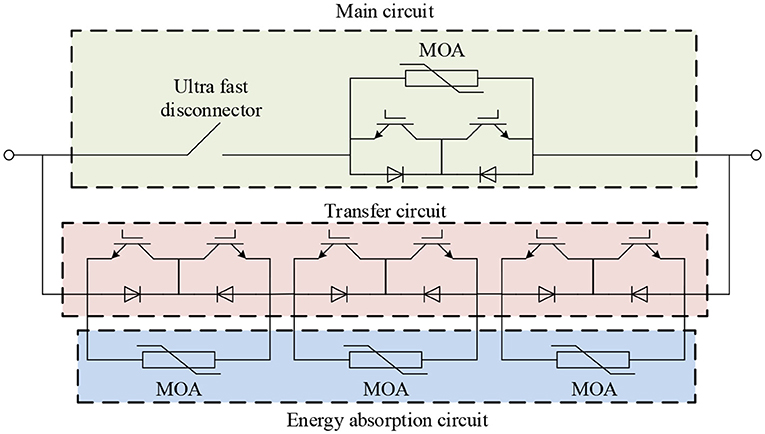
Figure 4. Hybrid DC breaker of ABB.
The DCCB consists of a main circuit, a transfer circuit, and an energy absorption circuit. The working current flows through the main circuit for power transmission. Once a DC fault occurs, the IGBT of the transfer circuit is turned on, and the IGBT of the main circuit is turned off immediately. When the current of the main branch decreases to zero, the mechanical switch will be opened, and then the IGBT of the transfer circuit is disconnected. Finally, the energy of the continuous current of the inductor is discharged through the arrester.
Because the DCCB has no inductance or capacitance, its external circuit presents pure resistance characteristics. In different working stages, its equivalent resistance, RDCCB, can be calculated using the following formula:
(a) Before the DC fault:
(b) During the fault current transfer:
(c) After the fault current transfer:
where NonM is the number of IGBT switches used in the main circuit and NonT is the number of IGBT switches used in the transfer circuit.
FCL Operation Mechanism and Equivalent Impedance Calculation
At present, passive FCL, connecting the smoothing reactor in series in the DC line, is widely used in engineering. The disadvantage of this method is that, if the smoothing reactor is too small, the DC fault current cannot be limited by it effectively. However, if the smoothing reactor is too large, the dynamic characteristics of the system will be reduced.
In the future, each DC line of the DC power grid should be equipped with active FCL as well as the smoothing reactor. At present, there is no recognized topology for the active FCL, but the existing research ideas are basically the same: control power electronic devices to make the fault current flow into a high inductance branch.
By analyzing and comparing the DCCB and active FCL, it can be concluded that their working modes are similar: a fault current transferred to another branch for current limiting or breaking. The method of analyzing the equivalent resistance RFCL and equivalent inductance LFCL of active FCL is basically the same as that of DCCB. However, FCLs also have inductance.
(a) Before the DC fault:
(b) During the fault current transfer:
(c) After the fault current transfer:
PSS-Equivalent Impedance Calculation
Based on the PHIL platform of the four-terminal flexible DC power grid as an example, the equivalent circuit of the two-terminal DC transmission system at PSS can be obtained through the above analysis, as shown in Figure 5.
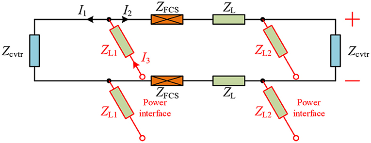
Figure 5. Equivalent model of PSS.
In Figure 5, the red line indicates the outgoing line of the PA, ZL is the DC transmission line impedance of the PSS subsystem, and ZFCS is the sum impedance of the DC fault current suppression equipment.
The equivalent impedance of the PSS subsystem at the left power interface is discussed below:
(a) When I1 > 0, I2 ≤ 0, and I3 > 0, or I1 < 0, I2 ≥ 0, and I3 < 0, the equivalent resistance, RH, and equivalent reactance, XH, of the PSS subsystem will be as follows:
(b) When I1 ≤ 0, I2 > 0, and I3 > 0, or I1 ≥ 0, I2 < 0, and I3 < 0, the equivalent resistance, RH, and equivalent reactance, XH, of the PSS subsystem will be as follows:
(c) When I1 > 0, I2 > 0, and I3 > 0, or I1 < 0, I2 < 0, and I3 < 0, the equivalent resistance, RH, and equivalent reactance, XH, of the PSS subsystem will be as follows:
Because the third term of RH and XH will be extremely small in (17), (two orders of magnitude smaller than the line impedance), the matching value of the damping impedance will remain almost unchanged during the transition between state (a) and state (c).
The equivalent resistance of the PSS subsystem at the right power interface can also be similarly calculated.
The Hall current sensors of the PSS subsystem feedback the above current signals back to the real-time digital simulator. The DSS system matches the left and right Z* according to different working conditions to ensure that Z* and (kU/kI)ZH are equal.
The value of RDCCB, RFCL, and LFCL is calculated by the PSS subsystem and transmitted back to the DSS subsystem through signal lines to calculate Z*.
Interface Delay Compensation Strategy
In the actual operation of the PHIL simulation platform, a time delay occurs in the feed forward channel of the interface hardware device because of the response time required by the PA, and, as a result, the voltage of the DSS subsystem cannot be reflected in the PSS subsystem in real time. In the steady state operation of the hybrid platform, the DC voltage remains constant, and the influence of interface delay can be ignored. However, if the DC bus voltage of the DSS subsystem fluctuates, the waveform of the DC voltage will get delayed on the PSS side. The delay may cause system instability, and then the cause of DCCB action (caused by overcurrent or delay) cannot be judged in the process of a fault test, so the delay must be compensated. But the DC signal fluctuation is random, so the frequency domain phase-shift method of the AC signals (Ren and Sloderbeck, 2011) cannot be used to compensate the DC interface delay. The time delays of each interface device used in the laboratory are shown in Table 1.
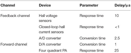
Table 1. Time delays of interface devices.
For the DC power interface, only the data prediction method can be used to compensate time delay. Based on the existing DC voltage data, the voltage value after Δt delay is predicted and the power amplifier is ordered to output the predicted voltage value.
Because the delay time, Δt, is microsecond physical quantity, which is only more than 10 times of the simulation step size of the DSS subsystem, a simple linear prediction method can be used. Based on the voltage during the current simulation step and the voltage value of the previous step, the slope of the straight line determined by these two points can be calculated, and the preliminary predicted value Udc_f of the DC voltage after Δt can be found.
An error will still exist between the preliminary predicted voltage and the actual DC voltage of the digital system. To compensate for this error, the predictive value can be defined as:
where Udc_PSS is the real-time output voltage of PA, Udc_DSS is the real-time DC bus voltage of the DSS subsystem, and k is the error compensation coefficient. Because the current compensation can be applied only to the physical side after a time delay of Δt, the error has been reduced, owing to the action of Udc_f. Thus, k should be a positive number <1. Figure 6 shows the schematic diagram of the interface delay compensation strategy.
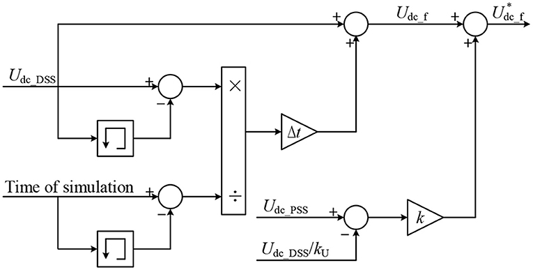
Figure 6. Diagram of the interface delay compensation strategy.
Simulation and Test
To verify the proposed power interface algorithm and interface delay compensation method, a digital and physical hybrid simulation platform for a four-terminal flexible DC power grid with DCCBs has been built. A 200 level ± 500 kV DSS subsystem, with 3,000 MW capacity, has been built in the computer by using MATLAB/SIMULINK. The DSS subsystem is connected with a 2 kW 31 level ± 200 V PSS subsystem through an RT-LAB5600 real-time digital simulator and four quadrant PAs. The wiring diagram of the digital and physical hybrid simulation platform has been shown in Figure 1. The difference from Figure 1 is that the two DCCBs at the PSS subsystem are, respectively, configured at the positive pole of MMC1 and MMC2, and the negative pole is not connected with DCCB. The PSS subsystem is shown in Figure 7, and its parameters are shown in Table 2.
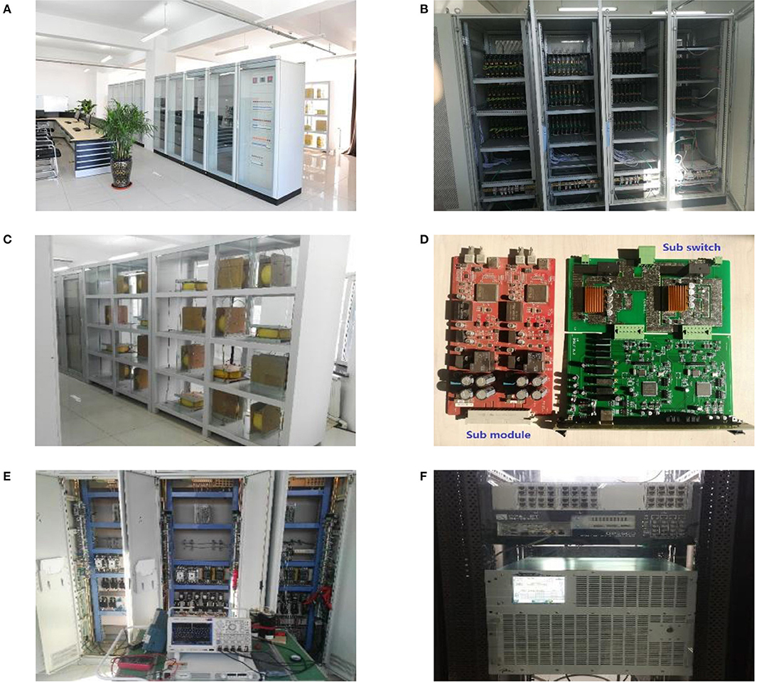
Figure 7. The test of power hardware in the loop. (A) Two terminal MMC-HVDC prototype, (B) prototype of DCCB, (C) DC line and arm reactance, (D) MMC sub-module and DCCB sub-switch, (E) experimental test platform, and (F) RT-LAB 5,600 and power amplifier.
Table 2. Experimental parameters of physical system.
Each board in Figure 7D contains two sub-modules or two sub switches. According to the system parameters, the ratio coefficient Ku of the controlled voltage source is 2,500, and the proportional coefficient Ki of the controlled voltage source is 600. By consulting the equipment manual and measuring the circuit resistance, the relevant parameters are calculated. As for MMC Rcvtr = 0.314 Ω, Lcvtr = 10.67 mH; as for DC line RL = RL1 = RL2 =1.92 Ω, LL = LL1 = LL2 = 63 mH; as for DCCB NonM = 15, NonT = 72, RTon + RDon = 0.03 Ω.
Experimental Condition 1: Verification of Interface Delay Compensation Algorithm
In the initial state, the system runs stably with a stable DC voltage at the rated value. When the DC voltage at the digital side is slightly disturbed, the comparison between the output voltage of the PA and the voltage of the DC line on the digital side before and after the delay compensation is shown in Figure 8A. The interface delay is about 30 μs, which is slightly higher than the forward channel delay. When a single pole short circuit occurs on the DC bus of the digital side, the prediction of the DC bus voltage by the interface delay compensation algorithm is shown in Figure 8B. Because the system adopts a symmetrical single-pole connection mode, there is no fault current exists on the DC side after the single pole-grounding short circuit, and the DCCBs equipment does not act. The experimental data show that, after using the delay compensation algorithm, the DSS outputs the predicted DC bus voltage in advance, and that the output voltage of the power amplifier can coincide with the DC line voltage of the digital side, which can reduce the error caused by the delay.
Figure 8. Verification of interface delay compensation algorithm. (A) Small interference test. (B) DC single pole short circuit test.
Experimental Condition 2: Transmission Power Change of the MMC Station
According to the number of the MMC station in Figure 1, MMC station I (DC voltage control) operates at Udc = 1 (unit value); MMC station II (active power control) operates at PII = 0 (unit value); MMC station III (droop control) operates at PIII = 0.3 (unit value); MMC station IV (droop control) operates at PIV = 0.3 (unit value). After the system is stable, the active power received by MMC station II will be raised once every 2.5 s for three times, respectively set as PII = 0, PII = −0.2, PII = −0.5, and PII = −0.8. The resistance R* matching value is shown in Figure 9A, the inductance L* matching value is shown in Figure 9B, the DC side voltage and the current of MMC station II are shown in Figure 9C. When the system operates stably, the current and circulating current of upper and lower arms of the MMC station II of phase A are shown in Figure 9D, and the capacitor voltage of sub-module is shown in Figure 9E. The experimental data show that both sides of the power interface can achieve real-time impedance matching. The MMC station has a high response speed to the change of active power. The voltage fluctuation of the sub-module capacitor is ~±0.4 V, which is within ±5% of the rated value.
Figure 9. The test of transmission power change. (A) R* matching value, (B) L* matching value, (C) DC voltage and current of MMC station II, (D) current and circulating current of phase A arms, and (E) capacitor voltage of sub module of MMC station II.
Experimental Condition 3: Blocking Test of the MMC Station
In the initial state, MMC station I operates at Udc = 1; MMC station II operates at PII = −0.8; MMC station III operates at PIII = 0.3; and MMC station IV operates at PIV = 0.3. When the system is stable, MMC station I will be locked and will not undertake the task of DC voltage control. The DC side voltage and the current of MMC station II before and after blocking are shown in Figure 10A, while those of MMC station III and MMC station IV are shown in Figure 10B. The experimental data show that the DC voltage decreases at the moment when MMC station I is blocked, but that MMC station III and MMC station IV can quickly stabilize the DC voltage to the rated value and provide the missing active power to maintain the stable operation of the system.
Figure 10. The test of MMC station locking. (A) DC voltage and current of MMC station II; (B) DC voltage and current of MMC station III and IV.
Experimental Condition 4: Bipolar Short Circuit Experiment on Physical Side
Before the fault, MMC station I operates at Udc = 1; MMC station II operates at PII = −0.7; MMC station III operates at PIII = 0.3; and MMC station IV operates at PIV = 0.3. After the system becomes stable, a bipolar short circuit fault occurs on the DC line between MMC station I and MMC station II. The voltage and current waveforms of the DC line are shown in Figure 11A, the resistance R* and inductance L* matching values in this process are shown in Figures 11B,C, respectively. When the fault current on the physical side rises to about 10 A, the DCCB switches it off. The DCCB completes this action in ~6 min after the fault has occurred. After the DC fault, the matching value of R* decreases from 37.058 to 25.875 Ω, while that of L* decreases from 1094.5 to 787.52 mH. After the DCCB transfer circuit is turned on, the main circuit resistance and transfer circuit resistance are in parallel relationship, the matching value of R* decreases to 25.552 Ω; however, there is no inductance change in the process, and the matching value of L* remains unchanged. After the DCCB main circuit is disconnected, the matching value of R* increases to 33 Ω, while that of L* remains unchanged. After the DCCB transfer circuit is disconnected, the physical side DC line is completely disconnected, and the power interface can only interact with adjacent MMC stations, and the matching value of R* is reduced to 17.308 Ω, while that of L* matching value is reduced to 568.61 mH. During the operation of DCCB, the power interface can match the impedance of the physical side in real time.
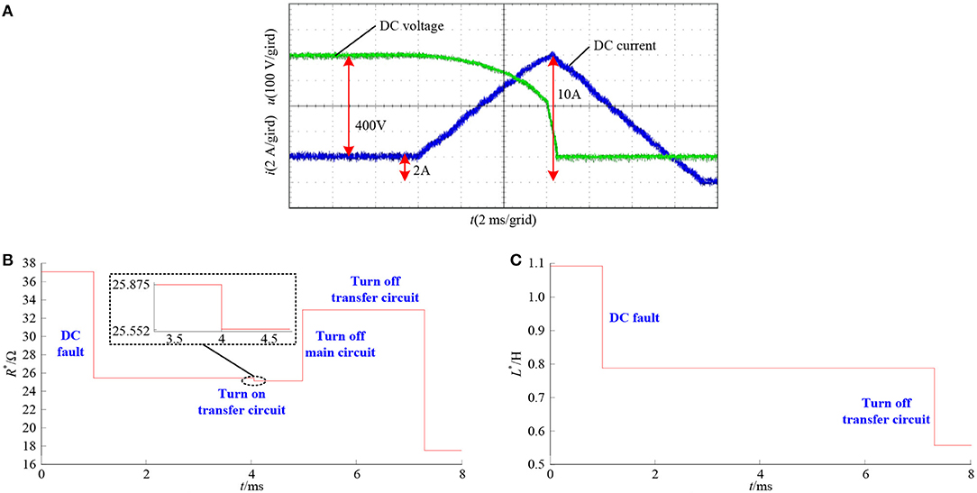
Figure 11. Bipolar fault test of PSS. (A) Voltage and current of the DC line at PSS, (B) R* matching value, and (C) L* matching value.
Conclusion
(a) In this paper, a simulation strategy based on the damping impedance interface algorithm is proposed for the digital and physical hybrid simulation platform of the HVDC grid with fault current suppression equipment. According to the working conditions of the physical system, the equivalent impedance of the physical system is calculated to realize the real-time matching of the damping impedance and ensure the stable operation of the hybrid simulation system.
(b) Because of the randomness of the DC signal fluctuation, the frequency domain phase shift method of the AC signal cannot be used for DC interface delay compensation. An interface delay compensation method for DC signal is proposed by this paper. It predicts the DC voltage of the DSS subsystem after a time of ΔT and outputs it in advance to realize interface delay compensation, which reduces the system error caused by the delay.
(c) A digital and physical hybrid simulation platform for the four-terminal flexible HVDC grid, with a DCCBs prototype, is built, which has verified the interface algorithm and the delay compensation method. In different experiment conditions, the interface delay is effectively compensated. When the working state of the system changes, the voltage and the current fluctuate slightly, but they can recover quickly and operate stably. After a DC short circuit fault, DCCB can complete the action in ~6 min, and the power interface can match the impedance change of the process in real time. It is proved that the interface control algorithm proposed in this paper is feasible.
At present, the PHIL platform in the laboratory only contains one type of fault current suppression equipment—DCCB. In the future, the FCL prototype will be installed in the PSS subsystem for DC fault current-limiting simulation.
Data Availability Statement
The original contributions presented in the study are included in the article/supplementary material, further inquiries can be directed to the corresponding author/s.
Author Contributions
WW is in charge of the method calculation, paper writing, system equivalence, and experiment. LW is in charge of statistics. BZ and GL are in charge of writing guidance. YX is in charge of the experimental guidance. SJ is in charge of modeling guidance. All authors contributed to the article and approved the submitted version.
Funding
This research was supported by the National Natural Science Foundation of China (U2066208).
Conflict of Interest
BZ was employed by company EHV Power Transmission Company Guangzhou Branch, China Southern Power Grid.
The remaining authors declare that the research was conducted in the absence of any commercial or financial relationships that could be construed as a potential conflict of interest.
References
Akagi, H. (2011). Classification, terminology, and application of the modular multilevel cascade converter. IEEE Trans. Power Electron 26, 3119–3130. doi: 10.1109/TPEL.2011.2143431
Dargahi, M., and Ghosh, A. (2014). Controlling current and voltage type interfaces in powerhardware-in-the-loop simulations. IET Power Electron 7, 2618–2627. doi: 10.1049/iet-pel.2013.0848
Gnanarathna, U. N., Gole, A. M., and Jayasinghe, R. P. (2011). Efficient modeling of modular multilevel HVDC converters (MMC) on electromagnetic transient simulation programs. IEEE Trans. Power Deliv 26, 316–324. doi: 10.1109/TPWRD.2010.2060737
He, Z., Wang, W., Gu, H., Li, G., Xin, Y., and Wang, Z. (2020). Development status and prospect of integrated key equipment of DC power grid with fault current limiting and breaking functions. Proc. CSEE. 40 3402–3417. doi: 10.13334/j.0258-8013.pcsee.200052
Hu, T., Zhu, Y., Yin, Y., Jiang, W., and Li, F. (2012). Modeling and study of digital/analog hybrid simulation forbulk grid with multi-analog HVDC simulators. Proc. CSEE 32, 68–75. doi: 10.13334/j.0258-8013.pcsee.2012.07.010
Jiang, S., Xin, Y., Li, G., and Wang, L. (2020). A novel DC fault ride-through method for wind farms connected to the grid through bipolar MMC-HVDC transmission. [OL] IEEE Trans. Power Deliv. 35, 2937–2950. doi: 10.1109/TPWRD.2020.2991722
Kotsampopoulos, P., Lehfuss, F., and Lauss, G. (2015). The limitations of digital simulation and theadvantages of PHIL testing in studying distributed generation provision of ancillaryservices. IEEE Trans. Ind. Electron. 62, 5502–5515. doi: 10.1109/TIE.2015.2414899
Li, S., Xu, J., Lu, Y., Zhao, C., Zhang, J., Jiang, C., et al. (2019). An auxiliary DC circuit breaker utilizingan augmented MMC. IEEE Trans. Power Deliv. 34, 561–571. doi: 10.1109/TPWRD.2019.2892445
Li, G., Wang, W., He, Z., Xin, Y., and Gu, H. (2020). Multi-port inductively coupled HVDC current limiting circuit breaker. Power System Techn, 40, 3866–3875. doi: 10.13335/j.1000-3673.pst.2019.2197
Majumder, R., Auddy, S., Berggren, B., Velotto, G., Barupati, P., Jonsson, T., et al. (2017). An alternative method to build DC switchyard with hybrid DC breaker for DC grid. IEEE Trans. Power Deliv. 32, 713–722. doi: 10.1109/TPWRD.2016.2582923
Matar, M., Paradis, D., and Iravani, R. (2016). Real-time simulation of modular multilevel convertersfor controller hardware-in-the-loop testing. IET Power Electron 9, 42–50. doi: 10.1049/iet-pel.2015.0012
Paran, S., Fleming, F., Li, D., and Edrington, C. S. (2014). “Utilization of adaptive PHIL interfaces for harmonicload cases,” in IECON Annual Conference of IEEE Industrial Electronics Society, (Dallas, TX: IEEE), 3803–3808. doi: 10.1109/IECON.2014.7049066
Ren, W., and Sloderbeck, M. (2011). Interfacing issues in real-time digital simulators. IEEE Trans. Power Deliv. 26, 1221–1230. doi: 10.1109/TPWRD.2010.2072792
Ren, W., Steurer, M., and Baldwin, T. L. (2008). Improve the stability and the accuracy of powerhardware-in-the-loop simulation by selecting appropriate interface algorithms. IEEE Trans. IndAppl. 44, 1286–1294. doi: 10.1109/TIA.2008.926240
Steurer, M., Edrington, C. S., Sloderbeck, M., Ren, W., and Langston, J. (2010). A megawatt-scale power hardware-inthe-loop simulation setup for motor drives. IEEE Trans. Ind. Electron 57, 1254–1260. doi: 10.1109/TIE.2009.2036639
Teeuwsen, S. P. (2011). “Modeling the trans-bay cable project as voltage-sourced converter with modular multilevel converter design,” in 2011 IEEE Power and Energy Society General Meeting, (Detroit, MI: IEEE), 1–8. doi: 10.1109/PES.2011.6038903
Keywords: DC circuit breakers, damping impedance, DC power grid, power interface algorithm, power interface delay
Citation: Wang W, Wang L, Zhu B, Li G, Xin Y and Jiang S (2021) Construction of a Digital and Physical Hybrid Simulation Platform for MMC-HVDC Grid With Fault Current Suppression Equipment. Front. Energy Res. 9:660236. doi: 10.3389/fenrg.2021.660236
Received: 29 January 2021; Accepted: 07 April 2021;
Published: 03 May 2021.
Edited by:
Nestor Francisco Guerrero-Rodriguez, Pontificia Universidad Católica Madre y Maestra, Dominican RepublicReviewed by:
Pengfei Tu, Nanyang Technological University, SingaporeKenneth E. Okedu, National University of Science and Technology (Muscat), Oman
Copyright © 2021 Wang, Wang, Zhu, Li, Xin and Jiang. This is an open-access article distributed under the terms of the Creative Commons Attribution License (CC BY). The use, distribution or reproduction in other forums is permitted, provided the original author(s) and the copyright owner(s) are credited and that the original publication in this journal is cited, in accordance with accepted academic practice. No use, distribution or reproduction is permitted which does not comply with these terms.
*Correspondence: Limeng Wang, NDI1OTQ0MjA2QHFxLmNvbQ==