 Danilo Santoro
 Nicola Delmonte
 Paolo Cova
 Andrea Toscani
- Department of Engineering and Architecture, University of Parma, Parma, Italy
The increased use of DC renewable energy resources and DC storage systems, combined with the necessary reduction of energy waste, is boosting the development of DC smart grids. In this scenario, DC load emulation is of great importance. From the hardware point of view, DC buses stability of smart grids and the different DC/DC converter topologies must be tested. From the software point of view, smart grid strategies and job schedulers must be tested with different power absorption profiles. Moreover, DC load emulation can be useful for many other purposes, such as battery characterization, power supply testing, photovoltaic I-V curve measurements, etc. In this work, a cost-efficient DC Active Load (AL) solution is proposed. The principle of the circuit topology is a buck-boost-derived converter. This solution can be designed and tested considering the required voltage, current, and maximum input power. Both simulation and experimental results are shown on a 400 W size prototype. Thermal and electrical results validate the simulation model and the AL feasibility.
Introduction
The shift towards the use of renewable energy resources and storage systems boosted the research and development of smart grids with DC buses and small DC/DC voltage converters as point-of-load interfaces. In the literature, different grid architectures can be found with a 48 V DC bus and small DC/DC voltage converters (Kumar et al., 2019; Moussa et al., 2019). Moreover, different control strategies can be applied, i.e. conventional droop control, virtual-resistance-based droop control, and adaptive droop control (Singh et al., 2019). In this scenario, multiple programmable active loads are of great importance for tests with varying power absorption profiles (e.g., for dynamic performance analysis (Zaitsev, 2021; Fu et al., 2022). Constant resistive loads are often unsuitable to ensure a full scenario test of smart grids, particularly for smart control strategies that consider the time-variant power absorption of the connected loads. Moreover, the design of the point-of-load DC/DC converters can sensibly change with the desired output voltage and power ratings. Thereby, this paper proposes a cost-efficient AL solution that can be programmed for a time-varying scenario.
Historically, ALs, known also as electronic loads, are used to test power converters. In comparison to the fixed load impedances, using ALs, a dynamic load change can be emulated to evaluate the converter performances in terms of disturbance rejection. However, in this case, the thermal management of the electronic loads is not an issue due to short-time tests. In the literature, many topologies of AL can be found. Often, they are dissipative and they are made to behave as variable resistors (Rosas-Caro et al., 2009). With a programmable AL the flexibility is higher and many features of a power converter under test, such as load regulation, power supply ratings, and overcurrent protection, can be properly and smoothly tested. Moreover, ALs can be used to test the capacity of batteries (Rathy and Balaji, 2018).
Another very useful application is the testing of power converters to supply digital systems such as microcontrollers or solid-state drives (Williams, 2011; Manjunath I and Dr. V Chayapathy, 2017). Here, a power MOSFET is switched to evaluate the current slew rate with a step load variation.
With the diffusion of smart grids, the use of ALs has been extended. They are used both for AC (single and 3-phase) and DC characterizations of power converters, sources, and buses (Serban et al., 2006; Tsang and Chan, 2012; Peng et al., 2016; Geng et al., 2018; Kanadhiya and Bohra, 2018; Nujithra and Premarathne, 2018; Pudur and Srivastava, 2018; Serna-Montoya et al., 2019; Serna-Motoya et al., 2022). Typically, the ALs topologies for micro and nano grids are based on converters such as boost (Ayop et al., 2021), SEPIC (Vogman and Consulting, 2018), buck-boost (Meng-Ting et al., 2017), back-to-back (Li et al., 2008), and multilevel inverters (Niu et al., 2021).
In this work, an AL topology derived from the buck-boost power converter topology is proposed. The design criterium, unlike the typical one adopted for an interface power converter, is thought for increasing power dissipation. This is reached with a specifically added resistance and inductance on the input section. Working input voltage and power absorption ranges can be easily changed and adapted using the proposed topology.
The prototype has been designed for input voltages in the range 12÷48 V and absorbed currents up to 10 A. Simulations have been validated through experimental results to easily design scaled ALs. Both the static and dynamic behaviors of the AL prototype are shown.
Active load circuit topology
The topology of the proposed AL is a buck-boost-derived converter, as shown in Figure 1. For AL applications, high efficiency is not a requirement, for this reason, an improved input passive filter and an input resistance for power dissipation sharing are added, and the output capacitors are not sized to reduce the voltage ripple.
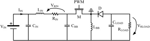
FIGURE 1. Active Load circuit topology.
The main power dissipation is obtained through the input resistance
Simulation model and component sizing
For the optimal components sizing, the AL has been simulated in MATLAB/Simulink environment using PLECS blockset for the buck-boost modified scheme. Figure 2 shows the simulation model, where the PLECS subsystem that contains the AL circuit topology is highlighted.
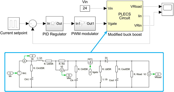
FIGURE 2. Active Load Simulation Model. The PLECS subsystem with the circuit model is highlighted.
The input resistor
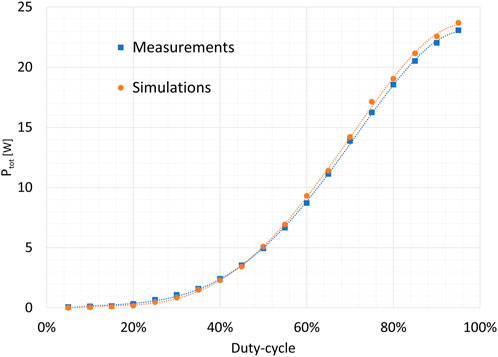
FIGURE 3. Total input absorbed power versus the duty-cycle at fixed input voltage Vin = 5 V.
As for the load resistor
For our application, with a 12 V input voltage, a 0.8 Ω input resistance, a 10 A required input current, and a power dissipated on the AL of approximately 400 W, the load resistance
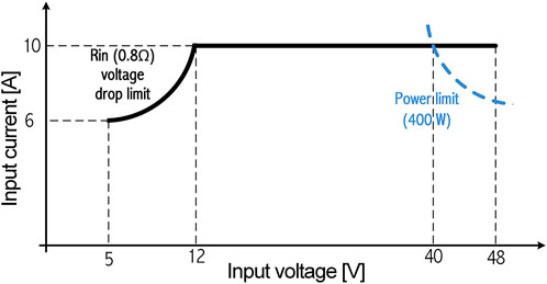
FIGURE 4. Operating V-I limits of the realized prototype.
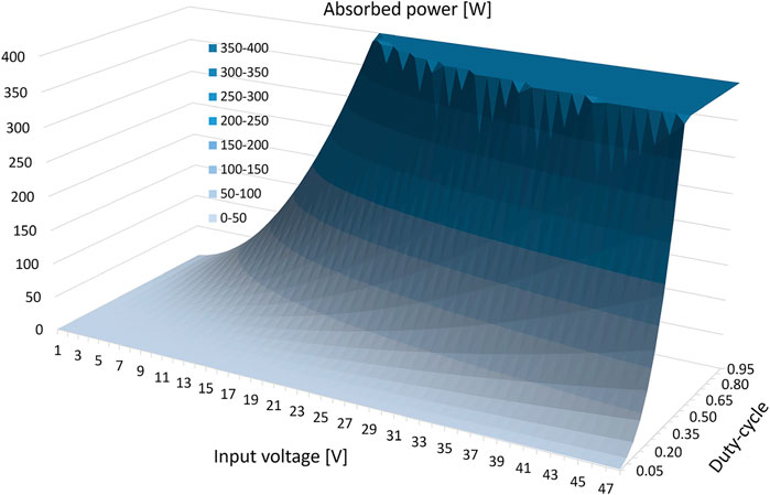
FIGURE 5. Surface plot of the total input absorbed power versus the input voltage and the duty-cycle.
Experimental prototype
To validate the simulations, an AL prototype has been developed. The test bench is shown in Figure 6.
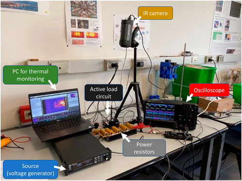
FIGURE 6. Active load circuit test bench.
The experimental test bench has been defined considering general purpose components already present in a laboratory, and with some layout considerations for a reduced maximum temperature on the circuit and an increased dissipated power. Considering that the power dissipated by the circuit is entirely transformed into heat, the thermal design is a critical issue. The power MOSFET, the diode, and the power resistors need heatsinks for dissipation. In this prototype, also fans have been added, contributing to increase the power dissipation by absorbing power themselves and allowing higher power ratings on the other devices. The fans are turned-on when the input voltage increases over 12 V, and they are fed using an integrated buck converter to reduce the input voltage to a regulated output voltage of 12 V. The two fans blow air on the heatsink of the MOSFET and on the heatsink connected to the input resistance.
The total cost of the proposed AL circuit is around 200 $. This can be considered a very competitive and cost-efficient solution since in the market the costs of programmable electronic loads with similar requirements vary from 750 $ to 1,500 $.
Simulation and experimental results
Simulations have been validated through experimental tests considering two scenarios: an open loop duty-cycle sweep of the PWM control signal with a constant input voltage and a closed loop input current control with a change of the set-point for the dynamic behavior validation.
Figure 7 shows the relation between the open loop duty-cycle and both dissipated power and input current with an input voltage of 24 V and as expected this trend is a monotonically increasing function. Waveforms obtained by simulation and measurement are compared.
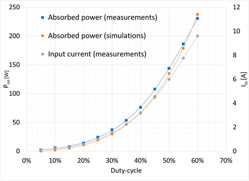
FIGURE 7. Total input absorbed power and input current versus the duty-cycle at fixed input voltage Vin = 24 V.
Figure 8 shows the thermal map with Vin = 40 V and dissipated power Pd = 400 W. The hottest temperatures are recorded on the input resistor, the load resistor, and the power MOSFET. High temperatures on the resistors indicate that these components are those where the main heat is generated to dissipate the electrical power absorbed by the AL. While on the MOSFET, the heating is mainly due to a smaller surface for the heat exchange, even though the power dissipated is almost two orders of magnitude smaller than the one on the resistors.
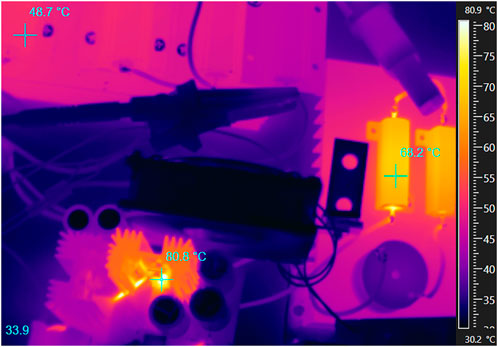
FIGURE 8. Active Load thermal map with input voltage Vin = 40 V and input current Iin = 10 A (Pd = 400 W).
Figure 9 shows the input voltage (blue), the input current (magenta), the voltage drop on the input resistance
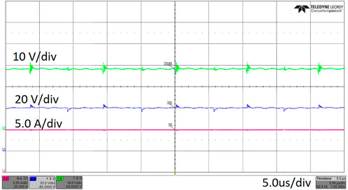
FIGURE 9. Oscilloscope capture with input voltage Vin = 40 V and input current Iin = 10 A (Pd = 400 W).
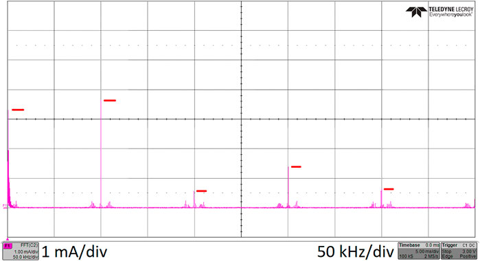
FIGURE 10. FFT of the input current (Iin = 10 A) with input voltage Vin = 40 V (Pd = 400 W).
The input current of the proposed buck-boost derived topology can be compared with a classic buck-boost converter. In Figure 11, the simulation results of the input current with two architectures are shown, namely the proposed topology and a buck-boost topology without input resistor and inductor, keeping all the other components with the same values. The high current ripple of the classic buck-boost is not suitable for an AL application.
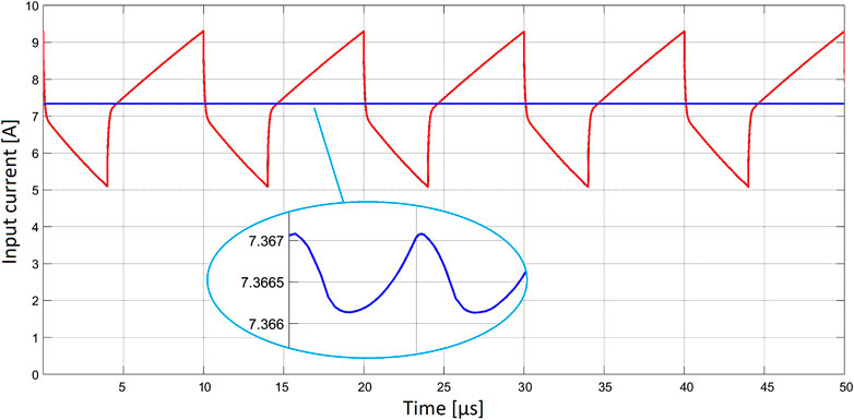
FIGURE 11. Input current comparison between the buck-boost-derived topology (blue) and typical buck-boost converter (red).
Finally, experimental tests on the prototype have been done to verify the dynamic behavior of the circuit, and results were compared with those obtained using the simulation model. Considering the same PI tuning values for the current control loop, and a 12 V input voltage, Figure 12 shows the simulation results (a) and experimental results (b) with a set-point changing from 0.5 A to 10 A, and from 10 A to 0.5 A. In this configuration, for a current step-up change, a settling time of about 12 m is measured. A higher circuit response time, mainly due to the time necessary to discharge the energy stored in the inductors and capacitors, can be observed for a current step-down change. In this case, a settling time of about 14 m is measured. In both cases, measurements can be compared with simulations, validating the model that can be used also to define the proportional-integral regulator fine tuning.
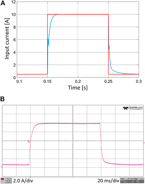
FIGURE 12. Simulation (A) end experimental (B) results of current step response from Iin = 0.5 A–10 A, with fixed input voltage Vin = 12 V.
The proposed solution can receive complex current set-point profiles from a PC via MATLAB environment. This operating principle can be used for large-scale emulations, where the microcontroller receives a parameterized set-point sequence at its input. The block diagram of the control algorithm is shown in Figure 13.

FIGURE 13. Block diagram of the Active Load control algorithm.
Finally, the circuit has been simulated and tested with an input voltage change from 18 V to 12 V, with a 4 A input current constant set-point. Simulation results (a) and experimental ones (b) are shown in Figure 14. These waveforms show a good input voltage change rejection.
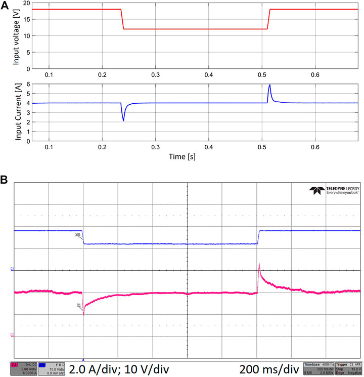
FIGURE 14. Simulation (A) and experimental (B) results with an input voltage change from Vin = 18 V–12 V, with constant input current set-point Iin = 4 A.
Conclusion
This work proposes a cost-efficient programmable DC AL. The DC AL can be used for DC load emulation, DC/DC converter tests, battery characterization, and in general for all the applications where an arbitrary and programmable current profile absorption is needed. For this realization, a buck-boost-derived topology has been adopted with general-purpose discrete components. The circuit is supervised by a microcontroller which can be interfaced with a PC via software for complex current profile load emulations.
Simulations have been used for sizing the components and have been validated through experimental measurements. The prototype has been characterized thermally and electrically. Static current absorption profiles and dynamic input current control behaviors have been first simulated, and then tested. The fabricated prototype works with input voltages from 12 V to 48 V, with input currents up to 10 A, and with a maximum power absorption of 400 W. The total cost of the prototype is around 200 $, which is very competitive with respect to the market available solutions.
Data availability statement
The raw data supporting the conclusion of this article will be made available by the authors, without undue reservation.
Author contributions
All authors listed have made a substantial, direct, and intellectual contribution to the work and approved it for publication.
Conflict of interest
The authors declare that the research was conducted in the absence of any commercial or financial relationships that could be construed as a potential conflict of interest.
Publisher’s note
All claims expressed in this article are solely those of the authors and do not necessarily represent those of their affiliated organizations, or those of the publisher, the editors and the reviewers. Any product that may be evaluated in this article, or claim that may be made by its manufacturer, is not guaranteed or endorsed by the publisher.
References
Ayop, R., Ayob, S. M., Tan, C. W., Sutikno, T., and Aziz, M. J. A. (2021). Comparison of electronic load using linear regulator and boost converter. Int. J. Power Electron. Drive Syst. 12, 1720–1728. doi:10.11591/ijpeds.v12.i3.pp1720-1728
Fu, S., Wang, C., Zhang, L., Chen, X., and Shu, Y. (2022). Optimized Control of active loads in DC microgrids with virtual energy storage. Energy Rep. 8, 13962–13969. doi:10.1016/j.egyr.2022.10.336
Geng, Z., Gu, D., Hong, T., and Czarkowski, D. (2018). Programmable electronic AC load based on a hybrid multilevel voltage source inverter. IEEE Trans. Ind. Appl. 54, 5512–5522. doi:10.1109/TIA.2018.2818059
Kanadhiya, M. C., and Bohra, S. S. (2018). “Simulation analysis of active programmable electronic AC load,” in Proceedings of the 2018 3rd International Conference for Convergence in Technology, Pune, India, April 2018, 1–6. doi:10.1109/I2CT.2018.8529804I2CT
Kumar, J., Agarwal, A., and Agarwal, V. (2019). A review on overall control of DC microgrids. J. Energy Storage 21, 113–138. doi:10.1016/j.est.2018.11.013
Li, F., Zou, Y. P., Wang, C. Z., Chen, W., Zhang, Y. C., and Zhang, J. “Research on AC electronic load based on back to back Single-phase PWM rectifiers,” in Proceedings of the IEEE Applied Power Electronics Conference and Exposition - APEC, Austin, TX, USA, February 2008, 630–634. doi:10.1109/APEC.2008.4522787
Manjunath, I., and V Chayapathy, Dr. (2017). Programmable DC electronic load for testing on-board voltage regulators. Int. J. Eng. Res. 6, 335–338. doi:10.17577/ijertv6is090166
Meng-Ting, Z., Ming-Yan, W., and Le-San, W. (2017). “Design and implementation of a multifunctional DC electronic load,” in Proceedings of the 2017 IEEE Transportation Electrification Conference and Expo, Asia-Pacific, ITEC Asia-Pacific, Harbin, China, August 2017, 1–6. doi:10.1109/ITEC-AP.2017.8080808
Moussa, S., Ghorbal, M. J. Ben, and Slama-Belkhodja, I. (2019). Bus voltage level choice for standalone residential DC nanogrid. Sustain. Cities Soc. 46, 101431. doi:10.1016/j.scs.2019.101431
Niu, J., Wang, J., Gao, Z., Martin, R. B., Giewont, W. B., and Wang, F. “Modular multilevel converter based reconfigurable Ac load emulator,” in Proceedings of the 2021 IEEE 12th Energy Conversion Congress & Exposition - Asia (ECCE-Asia), Singapore, May 2021, 438–442. doi:10.1109/ECCE-Asia49820.2021.9479089
Nujithra, T., and Premarathne, U. S. “Investigation of efficient heat dissipation mechanisms for programmable DC electronic load design,” in Proceedings of the 2018 8th International Conference on Power and Energy Systems, ICPES 2018, Colombo, Sri Lanka, December 2018 (IEEE), 201–206. doi:10.1109/ICPESYS.2018.8626879
Peng, J., Chen, Y., Fang, Y., and Jia, S. “Design of programmable DC electronic load,” in Proceedings of the 2016 International Conference on Industrial Informatics - Computing Technology, Intelligent Technology, Industrial Information Integration, ICIICII 2016, Wuhan, China, December 2016 (IEEE), 351–355. doi:10.1109/ICIICII.2016.0090
Pudur, R., and Srivastava, V. K. “Performance study of electronic load controller for integrated renewable sources,” in Proceedings of the 2018 2nd International Conference on Electronics, Materials Engineering and Nano-Technology, IEMENTech 2018 (IEEE), Kolkata, India, May 2018, 1–6. doi:10.1109/IEMENTECH.2018.8465144
Rathy, G. A., and Balaji, A. (2018). DC variable electronic load for SMPS testing. Int. Res. J. Eng. Technol. 5, 1070–1074.
Rosas-Caro, J. C., Peng, F. Z., Cha, H., and Rogers, C. (2009). Z-Source-Converter-Based energy-recycling zero-voltage electronic loads. IEEE Trans. Ind. Electron. 56, 4894–4902. doi:10.1109/tie.2009.2026374
Serban, I., Ion, C., Marinescu, C., and Cirstea, M. N. “Electronic load controller for stand-alone generating units with renewable energy sources,” in Proceedings of the IECON (Industrial Electronics Conference) (IEEE), Paris, France, November 2006, 4309–4312. doi:10.1109/IECON.2006.347688
Serna-Montoya, L. F., Cano-Quintero, J. B., Munoz-Galeano, N., and Lopez-Lezama, J. M. “Programmable electronic AC loads: A review on hardware topologies,” in Proceedings of the 2019 IEEE Workshop on Power Electronics and Power Quality Applications, PEPQA 2019 - Proceedings (IEEE), Manizales, Colombia, May 2019, 1–6. doi:10.1109/PEPQA.2019.8851542
Serna-Motoya, L. F., Ortiz-Castrillón, J. R., Gil-Vargas, P. A., Muñoz-Galeano, N., Cano-Quintero, J. B., and López-Lezama, J. M. (2022). Implementation of a programmable electronic load for equipment testing. Computers 11, 106–117. doi:10.3390/computers11070106
Singh, P., Paliwal, P., and Arya, A. (2019). A review on challenges and techniques for secondary control of microgrid. IOP Conf. Ser. Mat. Sci. Eng. 561, 012075. doi:10.1088/1757-899x/561/1/012075
Tsang, K. M., and Chan, W. L. (2012). Fast acting regenerative DC electronic load based on a SEPIC converter. IEEE Trans. Power Electron. 27, 269–275. doi:10.1109/TPEL.2011.2158446
Vogman, V., and Consulting, P. C. (2018). SEPIC converter simplifies design of smart electronic loads. Available at: http://www.how2power.com/pdf_view.php?url=/newsletters/1802/articles/H2PToday1802_design_Vogman.pdf.1. 7.
Williams, J. (2011). A closed-loop, wideband, 100A active load. CA, USA: Linear Technology. doi:10.1016/b978-0-12-397888-2.00003-1
Keywords: active load, power supply testing, cost-efficient, load emulation, fast prototyping, arbitrary current absorption, electronic load, thermal management
Citation: Santoro D, Delmonte N, Cova P and Toscani A (2022) A cost-efficient DC active load laboratory solution. Front. Energy Res. 10:1078010. doi: 10.3389/fenrg.2022.1078010
Received: 23 October 2022; Accepted: 30 November 2022;
Published: 14 December 2022.
Edited by:
Ningyi Dai, University of Macau, ChinaReviewed by:
Svk Naresh, National Institute of Technology, Andhra Pradesh, IndiaDavid Cabezuelo Romero, University of Mondragón, Spain
Copyright © 2022 Santoro, Delmonte, Cova and Toscani. This is an open-access article distributed under the terms of the Creative Commons Attribution License (CC BY). The use, distribution or reproduction in other forums is permitted, provided the original author(s) and the copyright owner(s) are credited and that the original publication in this journal is cited, in accordance with accepted academic practice. No use, distribution or reproduction is permitted which does not comply with these terms.
*Correspondence: Andrea Toscani, YW5kcmVhLnRvc2NhbmlAdW5pcHIuaXQ=
†These authors have contributed equally to this work and share first authorship