 Fengjie Li1
 Bin Wang
- 1College of Electronic Information, School of Basic Medicine, Micro-Nano Technology College, Qingdao University, Qingdao, China
- 2College of Science, North China Institute of Science and Technology, Yanjiao, China
The optical absorption device plays a crucial role as a component of the infrared astronomical telescope and possesses a significant impact on astronomical observations. A simple metamaterial absorber with substitutable middle materials is made for short-wave infrared sensing. The absorber is designed as a hollow square column, using a patterning approach for the top-layer structure of metamaterials. The absorption characteristics are verified using the impedance matching method, which involves extracting S-parameters and then performing inverse calculations to determine the absorber’s equivalent impedance. The result shows the highest absorption peak is at 3.25 μm, reaching 99.71%, with an impressive average absorption rate of 99.01% between 1.52 and 3.66 μm. The results demonstrate that this absorber shows polarization insensitivity while maintaining high absorption even at large angles of incidence. The distribution of the electromagnetic field within the absorber, the electromagnetic losses within individual layers, and their impact on the absorptive performance are analyzed in detail. Polarization angles, transverse magnetic polarization, and transverse electric polarization are further explored. The parameters of each layer have been discussed. An investigation of the intermediate dielectric layer has been conducted. The proposed absorber shows the potential to achieve exceptional absorption performance under various dielectric conditions, rendering it a promising candidate for use in astronomical observation, medical tests, infrared detection, invisible short-wave infrared systems, radar and various optical devices.
1 Introduction
The infrared telescope plays a crucial role in astronomical observation. (Honniball et al., 2022; Jakobsen et al., 2022). Infrared detection equipment assists researchers in discovering previously unknown stars, planets, and galaxies, as well as studying cosmic dust clouds and interstellar matter. As a crucial element of infrared detection equipment, the infrared absorber must not only possess high sensitivity, but also adhere to strict requirements regarding size, material and other factors. Metamaterials are a category of artificial composite materials with a subwavelength size (Bertoldi et al., 2017). In contrast to natural absorptive materials, metamaterials not only possess ultra-thin characteristics but also relatively small unit sizes. Metamaterial perfect absorbers (MPAS) can achieve exceptional electromagnetic characteristics by manipulating their shape, structural parameters, and periodic arrangement. This resolves the constraints imposed by the inherent electromagnetic properties of materials. Owing to advancements in nanotechnology, research on metamaterials has made significant progress and has attracted increasing public interest in recent years. Light plays a pivotal role in our lives. The understanding and investigation of light have significantly deepened alongside the advancements in science and technology. Maxwell’s equations reveal that light is a special form of electromagnetic wave from a mathematical perspective (Bliokh et al., 2016). The theoretical framework of electromagnetic waves has advanced significantly. Employing electromagnetic theory to investigate and explain optical phenomena has emerged as a reliable and effective methodology. MPAS demonstrate outstanding electromagnetic tunability and have garnered considerable attention in the field of optics.
In 2008, Landy and colleagues pioneered the design and implementation of MPAS within the millimeter-wave range (Landy et al., 2008). Over the last decade, many researchers have shown significant interest in the optical absorption properties of MPAS. The spectral research range of MPAS has been further expanded to include visible light (Cao et al., 2014; Lin et al., 2019), near-infrared (Ding et al., 2016; Lei et al., 2018), mid-infrared (Ma et al., 2013; Zhao et al., 2021; Li et al., 2023; Zhang et al., 2024), long-wavelength infrared (Ruan et al., 2021; Qin et al., 2022; Wang et al., 2024), terahertz (Liu and Song, 2021; Wang et al., 2022), and microwave (Hou et al., 2021; Xu et al., 2021) bands. Metamaterials have a wide range of applications in multiple fields, including solar energy absorption (Lin et al., 2020), filters (McCrindle et al., 2013), and imaging (Fan et al., 2017). Infrared sensors are an important component of thermal imagers and they can be used for military night vision reconnaissance (Gade and Moeslund, 2013). Infrared sensors can be used to detect biomolecules and prevent diseases, making them widely applicable in the medical field (Aslan et al., 2017). Infrared sensors can also be utilized for detecting combustion systems and are commonly employed in industrial settings (Goldenstein et al., 2017). As technological capabilities advance, the limitations of narrowband absorption are no longer sufficient to meet the demands of applications such as infrared detection and radar technology. In recent years, numerous research reports in the field of metamaterials have focused on achieving broadband absorption. Employing multilayer structures through stacking is an effective method for enhancing the absorption performance of MPAS. Su et al. utilized a combination of graphene and MgF2 as a set of materials and integrated them into a multilayer structure, leading to the attainment of high broadband absorption in the terahertz band (Su et al., 2015). They explained the importance of electromagnetic resonance in the absorption of light energy by analyzing the distribution of the electromagnetic field. Liu et al. employed tungsten nanospheres in conjunction with SiO2 as a set of materials for a metal-dielectric stack (Liu et al., 2017). They vertically assembled eight sets of metal-dielectric materials, achieving an absorption rate exceeding 90% across the visible light and near-infrared spectral ranges. The high absorption performance primarily arises from the presence of surface plasmon resonance and multilayer Fabry-Pérot (F-P) resonance cavities. Zou et al. employed a traditional metal-dielectric-metal structure with the Gosper curve as the top periodic pattern (Zou et al., 2020). The multi-size resonant coupling of the top periodic structure excites electric resonances at multiple wavelengths, resulting in high broadband absorption within the mid-infrared spectrum. Li et al. introduced a classic metal-insulator-metal (Cr-Al2O3-W) MIM structure (Li et al, 2022). The average absorption is 94.84% from 800 nm to 3,000 nm. The top layer featured a set of four metal rings, each of varying in size, used as periodic structures. The analysis of the electromagnetic field distribution reveals that localized plasmon resonance is a crucial factor that influences absorption performance across the entire desired wavelength range. Moreover, there are alternative approaches to achieve high broadband absorption in MPAS, such as incorporating metamaterial elements (Bakır et al., 2016; Khuyen et al., 2017) and utilizing unique materials like graphene (Li et al, 2022; Huang et al., 2022). Infrared technology is advancing towards interdisciplinary applications, and multi-band broadband absorption has the potential to broaden the range of applications for absorptive materials. Enhancing the absorption performance of MPAS remains a significant challenge, particularly in the context of achieving broadband absorption. While previous reports have described broadband absorbers in the short-wave infrared region, there is still potential for enhancing absorption performance. Previous studies on MPAS focused mainly on using fixed materials, providing limited alternative options. The substitutability of dielectric materials augments the absorber’s potential for broader and more adaptable applications in related fields.
The proposed metal-dielectric-metal (MDM) absorber consists of a hollow square column. The characteristics of the proposed absorber are analyzed using the Finite-Difference Time-Domain (FDTD) method (Qian et al., 2021). The results indicate that the average absorption of our proposed absorber is as high as 99.01% in the wavelength range from 1.52 to 3.66 μm, with absorption rates exceeding 90% between 1.22 and 3.92 μm. Based on the impedance matching theory, we investigate the relationship between the equivalent impedance of the absorber and the impedance of free space. Our findings demonstrate that surface plasmon resonance improves absorption performance. This is determined by studying the distribution of the electromagnetic field at the absorption peaks. Additionally, Fabry-Perot cavities are involved in the absorption of incident light. In this paper, we investigate the impact of structural parameters on absorption performance. Furthermore, we discuss the polarization angles and incident angles for both transverse magnetic (TM) and transverse electric (TE) polarizations. InP, SiO2, and Si3N4 can be used as alternative intermediate dielectric layers in addition to GaAs. The MPAS introduced in this paper exhibits polarization independence, insensitivity to wide incident angles, and broadband high absorption characteristics. We propose a broadband absorber with a periodic unit cell of hollow square columns based on a metal-dielectric-metal structure. The features of our proposed absorber position it for potential applications in various optical devices, such as astronomical observation, medical tests, and infrared detection.
2 Design and theory
The traditional metal-dielectric-metal (MDM) structure achieves excellent absorption performance in MPAS through the implementation of a distinctive periodic structure on the upper plane (Yu et al., 2018). We propose a hollow square column absorber based on the MDM structure. The array structure of the proposed MPAS is shown in Figure 1A. Figures 1B–D represents the unit cell, the top view, and the side view of MPAS, respectively. Our proposed MPAS consists of titanium (Ti) as the metal layer and gallium arsenide (GaAs) as the dielectric layer. The bottom section of the MPAS is constructed using Ti as the metal component. The metal substrate is a square column with equal length and width and a thickness of H3 = 260 nm. The proposed absorber comprises a central dielectric layer with a thickness denoted as H2 = 110 nm. The top layer consists of a periodic structure made of hollow square columns, constructed from titanium metal. The square column on the top layer has a side length denoted as L = 380 nm. The inner cavity within the proposed absorber possesses a radius denoted as R = 180 nm. The thickness (H1) of the top periodic structure is 550 nm. The unit size (P) of the absorber is 660 nm. The mesh size is set 5 nm × 5 nm × 5 nm.
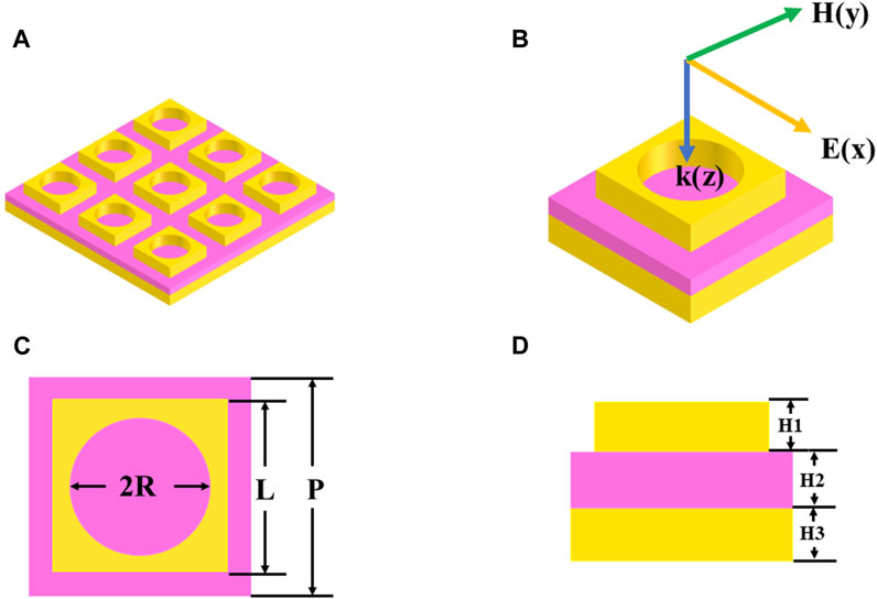
FIGURE 1. MPAS model structure. (A) Structural array of the proposed absorber. (B) 3D view of the unit structure. (C) Top view of the unit structure. (D) Side view of the unit structure.
In this paper, the proposed absorber is modeled using FDTD calculation software. Periodic boundary conditions are applied in the x and y directions, while a perfect absorbing layer is set up in the z direction. The simulation periodicity size is defined as 660 nm. A reflectance monitor (R(ω)) is positioned 2 μm above the absorber, while a transmittance monitor (T(ω)) is situated 2 μm below the absorber. We choose a plane wave as the incident light source for the absorber. As illustrated in Figure 1A, the incident light travels in the negative direction of the Z-axis, with the electric field oriented along the X-axis and the magnetic field along the Y-axis. The absorption rate can be expressed as A(ω) = 1- R(ω)- T(ω). The thickness of the lower metal reflector in the absorber significantly exceeds the skin depth of the incident light. Virtually no light waves can penetrate the absorber. The absorption can be expressed as A(ω) = 1- R(ω). Our proposed MPAS consists of titanium (Ti) as the arsenide (GaAs) as the dielectric layer. Data for both Ti and GaAs are sourced from Palik’s handbook (Palik, 1998). The real and imaginary components of the permittivity are shown in Figure 2. As an excellent lossy metal, Ti possesses a significantly large imaginary part of the permittivity in the infrared range, which enhances its absorption performance.
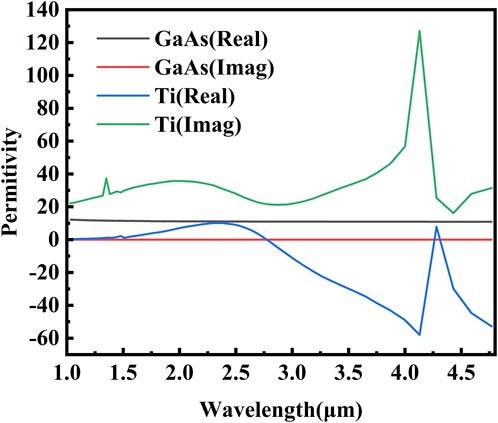
FIGURE 2. Permittivity data of Ti and GaAs.
We conduct extensive computational simulations and provide micromachining technology for the manufacturing and processes involved in this design. Ti film is deposited on a silicon substrate using ion beam sputtering. InP or GaAs thin films are deposited using Metal Organic Chemical Vapor Deposition (MOCVD). SiO2 or Si3N4 are deposited using Plasma Enhanced Chemical Vapor Deposition (PECVD). The high-precision photolithography steps transfer the designed pattern, while Inductively Coupled Plasma (ICP) technology is used to, etch this pattern.
The MPAS has the capability to adapt the effective impedance of the absorber to align with the free-space impedance by designing a unique top periodic structure that incorporates multi-size resonant coupling. This ensures that incident light is absorbed by the MPAS with minimal reflection back into free space. To verify its absorption characteristics, we extract the S-parameters of the proposed absorber. S11 and S21 denote the reflection and transmission values, respectively. Figure 3 illustrates the equivalent impedance of the absorber. By impedance matching theory, the closer the equivalent impedance of the absorber is to the free-space impedance, the higher the absorption performance (Jung et al., 2015; Huang et al., 2020):
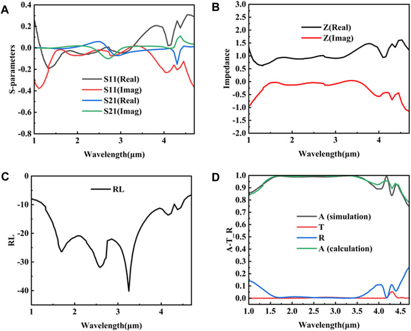
FIGURE 3. Parameter values of the absorber. (A) The values of S-parameters. (B) Equivalent impedance of the absorber. (C) The value of reflection loss. (D) Comparison of simulation and computational results. Absorption (A), Transmission (T) and Reflection (R) of the absorber.
In Eqs 1–4, Z represents the normalized equivalent impedance of the absorber, Γ is the reflection coefficient, RL signifies the reflection loss and A represents absorption. As depicted in Figure 3B, the real part of the equivalent impedance closely approximates 1, while the imaginary part tends toward zero within the wavelength range of 1.22 μm–3.92 μm. It indicates that the proposed absorber achieves impedance matching with free space, leading to absorption performance that closely approaches perfection. To visually understand the impact of impedance matching on reducing the reflection of incident light waves, we calculate the reflection coefficient (Γ) and reflection loss (RL) through the utilization of S-parameters. As shown in Figure 3C, the reflection loss registers below −10 dB across the wavelength range from 1.22 to 3.92 μm. As depicted in Figure 3D, the absorption rate exceeds 90% across the wavelength range from 1.22 to 3.92 μm, and the average absorption rate reaches an impressive 99.01% between 1.52 and 3.66 μm within the wavelength spectrum. The results obtained from the calculation of equivalent impedance are consistent with the simulation results. This further confirms the authenticity of the results. Three absorption peaks are observed at wavelengths of 1.73, 2.53, and 3.25 μm. The reflection loss is RL = −25.62 dB, the effective impedance is Z = 0.92–0.072i, and the absorption is A = 99.45% at 1.73 μm. The reflection loss is RL = −30.83 dB, the effective impedance is Z = 0.96–0.042i, and the absorption is A = 99.02% at 2.53 μm. The reflection loss is RL = −40.19 dB, the effective impedance is Z = 1.00–0.019i and the absorption is A = 99.71% at 3.25 μm.
To demonstrate the impact of the structure on absorption, we analyze the electromagnetic field distributions of the absorber at three absorption peaks. The incident light’s influence triggers collective oscillations among groups of free electrons at the metal-dielectric interface, ultimately leading to the formation of surface plasmon resonance (SPR) (Zhang et al., 2007; Chen et al., 2014):
In Eq. 5, P represents the unit size of the absorber, while i and j denote the order of SPR resonance. εd and εm stand for the permittivity values of the dielectric and metal, respectively. As shown in Figure 4, there is an electric field enhancement phenomenon occurring at the top layer. Electric field enhancement occurs at the four corners of the square column, while it is observed in the y-axis direction of a cylindrical cavity. The enhancement of the electric field in the top layer indicates the excitation of local surface plasmon resonance (LSPR), which contributes to absorption enhancement. The enhancement of the electric field within the cavity decreases progressively as the wavelength of light increases from 1.73 to 3.9 μm. The main factor contributing to absorption enhancement is the electric field enhancement induced by the LSPR at the outer boundary of the square pillar. Figures 5A–C shows the magnetic field distribution on the top layer. The magnetic field is primarily enhanced in the Y-axis direction within the cavity and at the boundary of the square pillar. Figures 5D–F shows the magnetic field distribution in the X-Z plane. It indicates that magnetic field enhancement occurs not only at the top layer but also at the intermediate dielectric layer. The increase in the magnetic field at the edge of the dielectric layer indicates the excitation of propagating surface plasmon resonance (PSPR). Both LSPR and PSPR synergistically enhance the absorption capabilities of our proposed absorber. Electromagnetic loss contributes to the absorption of incoming light. Figure 6 shows the energy consumption of the proposed absorber. This suggests that the primary cause of absorption is the electric loss from LSPR in the top layer, while the magnetic loss from PSPR in the middle dielectric layer also contributes to absorption.
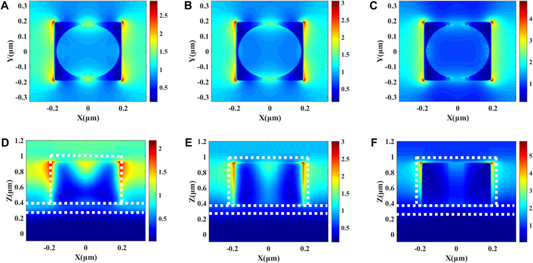
FIGURE 4. Electric field distribution at three absorption peaks. (A–C) Electric field distribution in the X-Y plane of the top layer at 1.73, 2.53 and 3.25 μm, respectively. (D–F) Electric field distribution in the X-Z plane at 1.73, 2.53 and 3.25 μm, respectively.
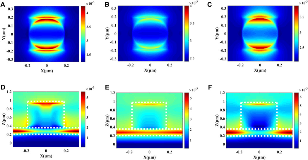
FIGURE 5. Magnetic field distribution at three absorption peaks. (A–C) Magnetic field distribution in the X-Y plane of the top layer at 1.73, 2.53 and 3.25 μm, respectively. (D–F) Magnetic field distribution in the X-Z plane at 1.73, 2.53 and 3.25 μm, respectively.
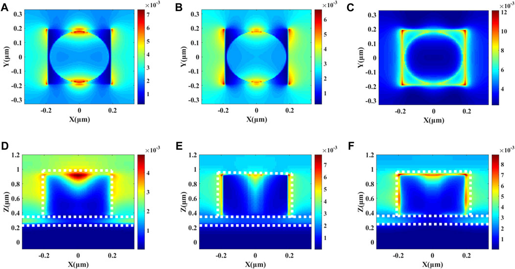
FIGURE 6. Power loss distribution at three absorption peaks. (A–C) Power loss distribution in the X-Y plane of the top layer at 1.73, 2.53 and 3.25 μm, respectively. (D–F) Power loss distribution in the X-Z plane at 1.73, 2.53 and 3.25 μm, respectively.
3 Results and discussion
The influence of the structural parameters on absorption performance is discussed. The structure and size of the absorber impact LSPR. Modifying the structural parameters can alter the electromagnetic properties of the absorber. By making precise adjustments to the relevant structural parameters, the performance of the absorber can be optimized. To explore the specific effects of various structural parameters on the absorption performance, the controlled variables method is employed. We modify the value of one parameter while keeping the other parameters constant. The top-layer periodic structure not only influences the impedance matching between the absorber and free space but also contributes to the absorption of incident light by inducing SPR. Figure 7 illustrates the impact of different parameter values in the top-layer structure on the absorption performance. As shown in Figure 7A, the cavity radius increases from 20 to 180 nm in increments of 40 nm. The absorption bandwidth undergoes a redshift as the cavity radius increases, while the absorption performance remains largely unchanged at longer wavelengths. Based on the electric field distribution depicted in Figure 4, it is evident that the LSPR at the cavity edge is significantly attenuated at longer wavelengths. As the wavelength redshifts, the electric field at the cavity edge gradually becomes stronger. As shown in Figure 7B, the side length (L) of the square pillar increases from 380 nm to 580 nm in increments of 50 nm. As L increases, the absorption performance steadily decreases across the entire wavelength range. The LSPR at the periphery of the square pillar significantly contributes to the absorption performance across the entire wavelength range. As L increases, it diminishes the plasma resonance at the periphery of the square pillar. On the other hand, the absorber experiences a greater impedance mismatch with free space. This leads to a higher reflection of incoming light back into free space, thereby reducing absorption performance. As shown in Figure 7C, when the thickness of the top layer increases from 350 to 550 nm, the average absorption gradually improves. However, the average absorption gradually decreases as the thickness increases from 550 to 750 nm, and the range of absorption exceeding 90% also diminishes. This indicates that both excessive and insufficient thickness of the top layer have adverse effects on plasmonic resonance. We selected a thickness of 550 nm as the optimal choice to achieve the best absorption performance.
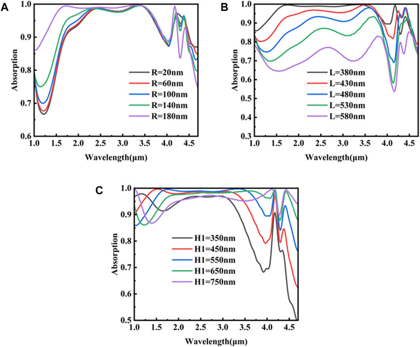
FIGURE 7. The impact of top layer structural parameters on the absorption performance. (A) The influence of cavity radius on the performance of absorption. (B) The influence of the top cube side length on the absorption performance. (C) The impact of the top layer thickness on the performance of the absorption.
The impact of dielectric thickness (H2) on absorption performance is depicted in Figure 8A. The H2 increases from 50 nm to 110 nm, leading to a gradual improvement in the average absorption rate and an expanded absorption bandwidth that exceeds 90%. When the dielectric layer thickness is increased from 110 nm to 170 nm, the average absorption rate progressively decreases. Based on the magnetic field distribution depicted in Figure 5, it is evident that PSPR occurs in the intermediate dielectric layer. This indicates that modifying the thickness of the dielectric layer can regulate PSPR and impact absorption performance. The reflection and interference of incident light between the top and bottom metal layers influence the configuration of the resonant cavity formed by the dielectric layer. Ultimately, we have chosen a thickness of 110 nm for the optimized dielectric layer. Figure 8B demonstrates the effect of unit size (P) on absorption performance. When p = 460 nm, the distance between adjacent top-layer periodic units is small. In addition to being influenced by incident light and LSPR, the cavity pillar of the top layer also experiences resonance coupling with the surrounding adjacent periodic units. This phenomenon leads to changes in the LSPR of each cavity pillar, ultimately reducing its absorption performance. When P increments from 560 nm to 860 nm in 100 nm intervals, there is a redshift in the absorption bandwidth. The range of wavelengths where absorption exceeds 90% decreases. The impact of different dielectrics on absorption performance is described in Figure 9. By fine-tuning the structural parameters, high absorption in the near-infrared to mid-infrared wavelength range is achieved using the same fundamental structure. The structural parameters of our proposed absorber with interchangeable materials are presented in Table 1. The substitutive capability of the dielectric material within the same structure significantly enhances the versatility of the absorber. The proposed absorber demonstrates an absorption rate of over 95% with four different dielectric materials. Therefore, we conclude that the proposed absorber demonstrates material substitution characteristics. As shown in Figures 10A, D, the polarization angles of the vertically incident light vary from 0° to 90°. The absorption performance of the top periodic structure is unaffected by the polarization angle due to its hollow square column shape, which is centrally symmetric. The polarization angles and incident angles of the incident light can vary significantly. Therefore, designing an absorber that is insensitive to changes in polarization angles and incident angles can accommodate various complex conditions. As shown in Figures 10B, E, the incident angles for TE polarization increase from 0° to 60°. As the incident angles increase, the absorption performance gradually decreases, and the absorption bandwidth undergoes a redshift. An absorption rate exceeding 90% is achieved within the bandwidth ranging from 1 μm to 3.47 μm when θ = 50°. However, the absorption sharply decreases when θ = 60°. As shown in Figures 10C, F, the TM polarization incident angles increase from 0° to 60°. With the increase in polarization angle, the absorption performance gradually decreases within the wavelength range of 1μm–4.7 μm. Even when θ = 60°, the absorption rate remains above 80%. The proposed absorber is insensitive to both TE and TM polarization angles. As shown in Table 2, our proposed absorber demonstrates excellent performance and material substitutability.
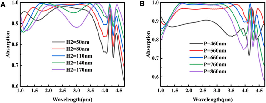
FIGURE 8. The influence of the dielectric layer and unit size on the performance of the absorption. (A) The influence of the dielectric layer thickness on the performance of absorption. (B) The effect of unit size on the performance of absorption.
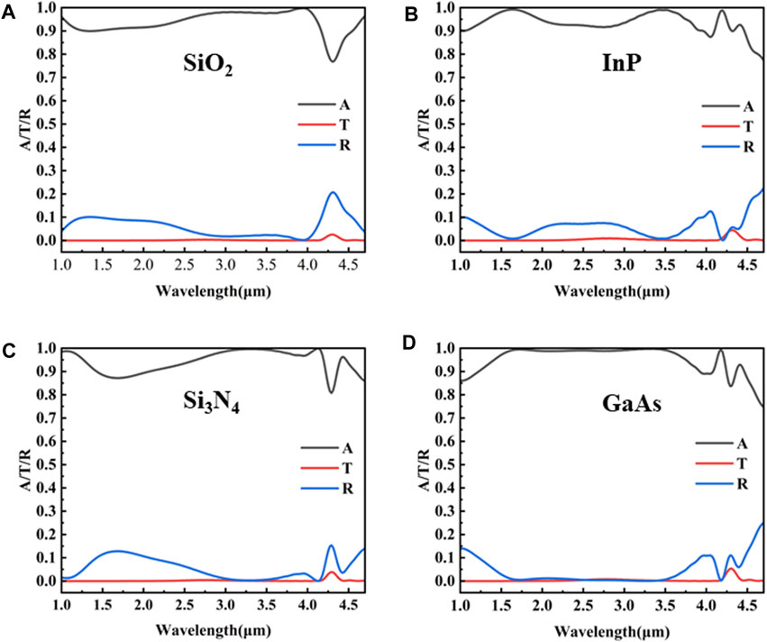
FIGURE 9. The absorption spectrum varies with different dielectrics based on the same hollow square column structure. (A) The absorption spectrum with a SiO2 dielectric layer. (B) The absorption spectrum with an InP dielectric layer. (C) The absorption spectrum with a Si3N4 dielectric layer. (D) The absorption spectrum with a GaAs dielectric layer.
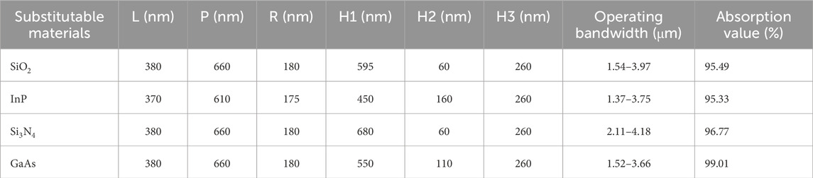
TABLE 1. The parameters of the absorber with substitutable materials.
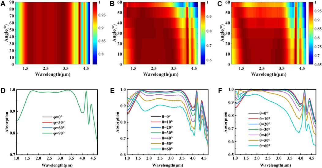
FIGURE 10. The influence of polarization angle (φ) and incident angle (θ). (A, D) The absorption spectrum with the polarization angle ranging from 0° to 90°. (B, E) The absorption spectrum with the incident angle ranging from 0° to 90° for TE polarization. (C, F) The absorption spectrum with the incident angle ranging from 0° to 90° for TM polarization.
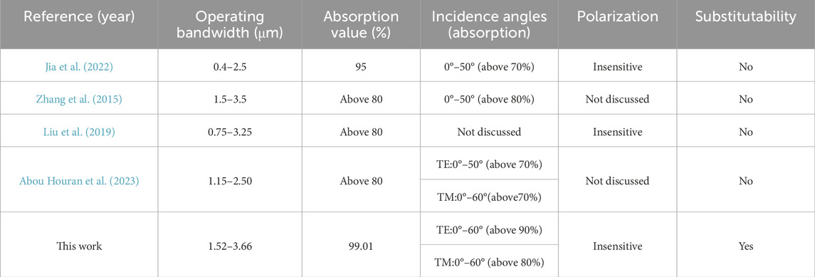
TABLE 2. Reports about broadband infrared absorber.
4 Conclusion
We proposed an absorber with a hollow square column based on the MDM structure. The average absorption is 99.01% within the wavelength range of 1.52–3.66 μm, with the highest absorption reaching 99.71% at 3.25 μm. The proposed absorber consists of a single metal material (Ti) and a single dielectric material (GaAs). The absorption curve has been verified and fits well based on impedance matching theory. Additionally, we investigated the distribution of the electromagnetic field at three absorption peaks, revealing the contribution of plasmonic resonances to the absorption performance. There is a regulating effect on the electromagnetic properties for structural parameters. We calculate the impact of the structural parameters of each part of the absorber on the absorption performance and determine the optimal parameter values. The study examines the impact of various dielectric materials on the performance of the absorber. By adjusting the structural parameters of the absorber while keeping the basic design unchanged, the substitution of different dielectric materials allows the absorber to maintain exceptional performance, achieving over 95% absorption. The proposed absorber is insensitive to polarization angles. Under TE and TM polarizations, with incident angles less than 50°, the absorption rate remains above 90%. A new structure that we proposed achieves near-perfect absorption in the short-wave infrared region. The substitutability of dielectrics allows the proposed absorber to have a wider range of potential applications in optical devices.
Data availability statement
The original contributions presented in the study are included in the article/Supplementary material, further inquiries can be directed to the corresponding authors.
Author contributions
FL: Formal Analysis, Writing–original draft, Writing–review and editing. SW: Software, Writing–original draft. ZC: Investigation, Writing–original draft. TZ: Data curation, Writing–original draft. RY: Project administration, Writing–original draft. BW: Supervision, Writing–review and editing. NL: Writing–review and editing.
Funding
The author(s) declare financial support was received for the research, authorship, and/or publication of this article. This work was supported by Qingdao Postdoctoral Application Research Project, the Chinese Ministry of Education’s Industry School Cooperation Collaborative Education Project: 220606513074515.
Conflict of interest
The authors declare that the research was conducted in the absence of any commercial or financial relationships that could be construed as a potential conflict of interest.
Publisher’s note
All claims expressed in this article are solely those of the authors and do not necessarily represent those of their affiliated organizations, or those of the publisher, the editors and the reviewers. Any product that may be evaluated in this article, or claim that may be made by its manufacturer, is not guaranteed or endorsed by the publisher.
Supplementary material
The Supplementary Material for this article can be found online at: https://www.frontiersin.org/articles/10.3389/fspas.2024.1374951/full#supplementary-material
References
Abou Houran, M., Armghan, A., Baqir, M. A., Aliqab, K., Saqlain, M., and Alsharari, M. (2023). MXene nanorods-based metasurface wideband absorber for infrared regime. Int. J. Therm. Sci. 193, 108452. doi:10.1016/j.ijthermalsci.2023.108452
Aslan, E., Kaya, S., Aslan, E., Korkmaz, S., Saracoglu, O. G., and Turkmen, M. (2017). Polarization insensitive plasmonic perfect absorber with coupled antisymmetric nanorod array. Sensors Actuators B Chem. 243, 617–625. doi:10.1016/j.snb.2016.12.030
Bakır, M., Karaaslan, M., Dincer, F., Delihacioglu, K., and Sabah, C. (2016). Tunable perfect metamaterial absorber and sensor applications. J. Mater. Sci. Mater. Electron. 27 (11), 12091–12099. doi:10.1007/s10854-016-5359-7
Bertoldi, K., Vitelli, V., Christensen, J., and Hecke, M. V. (2017). Flexible mechanical metamaterials. Nat. Rev. Mater. 2 (11), 17066. doi:10.1038/natrevmats.2017.66
Bliokh, K. Y., Bekshaev, A. Y., and Nori, F. (2016). Corrigendum: dual electromagnetism: helicity, spin, momentum, and angular momentum. New J. Phys. 18 (8), 089503. doi:10.1088/1367-2630/18/8/089503
Cao, T., Wei, C. W., Simpson, R. E., Zhang, L., and Cryan, M. J. (2014). Broadband polarization-independent perfect absorber using a phase-change metamaterial at visible frequencies. Sci. Rep. 4, 3955. doi:10.1038/srep03955
Chen, S., Meng, L., Hu, J., and Yang, Z. (2014). Fano interference between higher localized and propagating surface plasmon modes in nanovoid arrays. Plasmonics 10 (1), 71–76. doi:10.1007/s11468-014-9779-z
Ding, F., Dai, J., Chen, Y., Zhu, J., Jin, Y., and Bozhevolnyi, S. I. (2016). Broadband near-infrared metamaterial absorbers utilizing highly lossy metals. Sci. Rep. 6, 39445. doi:10.1038/srep39445
Fan, K., Suen, J. Y., Liu, X., and Padilla, W. J. (2017). All-dielectric metasurface absorbers for uncooled terahertz imaging. Optica 4 (6), 601. doi:10.1364/optica.4.000601
Gade, R., and Moeslund, T. B. (2013). Thermal cameras and applications: a survey. Mach. Vis. Appl. 25 (1), 245–262. doi:10.1007/s00138-013-0570-5
Goldenstein, C. S., Spearrin, R. M., Jeffries, J. B., and Hanson, R. K. (2017). Infrared laser-absorption sensing for combustion gases. Prog. Energy Combust. Sci. 60, 132–176. doi:10.1016/j.pecs.2016.12.002
Honniball, C. I., Lucey, P. G., Arredondo, A., Reach, W. T., and Malaret, E. R. (2022). Regional map of molecular water at high southern latitudes on the moon using 6 μm data from the stratospheric observatory for infrared Astronomy. Geophys. Res. Lett. 49 (9), 97786. doi:10.1029/2022gl097786
Hou, T., Jia, Z., Feng, A., Zhou, Z., Liu, X., Lv, H., et al. (2021). Hierarchical composite of biomass derived magnetic carbon framework and phytic acid doped polyanilne with prominent electromagnetic wave absorption capacity. J. Mater. Sci. Technol. 68, 61–69. doi:10.1016/j.jmst.2020.06.046
Huang, J., Li, J., Yang, Y., Li, J., Li, J., Zhang, Y., et al. (2020). Broadband terahertz absorber with a flexible, reconfigurable performance based on hybrid-patterned vanadium dioxide metasurfaces. Opt. Express 28 (12), 17832–17840. doi:10.1364/OE.394359
Huang, X., Cao, M., Wang, D., Li, X., Fan, J., and Li, X. (2022). Broadband polarization-insensitive and oblique-incidence terahertz metamaterial absorber with multi-layered graphene. Opt. Mater. Express 12 (2), 811. doi:10.1364/ome.451450
Jakobsen, P., Ferruit, P., Alves de Oliveira, C., Arribas, S., Bagnasco, G., Barho, R., et al. (2022). The near-infrared spectrograph (NIRSpec) on theJames WebbSpace telescope. Astronomy Astrophysics 661, A80. doi:10.1051/0004-6361/202142663
Jia, Y., Wu, T., Wang, G., Jiang, J., Miao, F., and Gao, Y. (2022). Visible and near-infrared broadband absorber based on Ti3C2Tx MXene-Wu. MXene-Wu. Nanomater. (Basel) 12 (16), 2753. doi:10.3390/nano12162753
Jung, J. Y., Lee, J., Choi, D. G., Choi, J. H., Jeong, J. H., Lee, E. S., et al. (2015). Wavelength-Selective infrared metasurface absorber for multispectral thermal detection. IEEE Photonics J. 7 (6), 1–10. doi:10.1109/jphot.2015.2504975
Khuyen, B. X., Tung, B. S., Yoo, Y. J., Kim, Y. J., Kim, K. W., Chen, L. Y., et al. (2017). Miniaturization for ultrathin metamaterial perfect absorber in the VHF band. Sci. Rep. 7, 45151. doi:10.1038/srep45151
Landy, N. I., Sajuyigbe, S., Mock, J. J., Smith, D. R., and Padilla, W. J. (2008). Perfect metamaterial absorber. Phys. Rev. Lett. 100 (20), 207402. doi:10.1103/PhysRevLett.100.207402
Lei, L., Li, S., Huang, H., Tao, K., and Xu, P. (2018). Ultra-broadband absorber from visible to near-infrared using plasmonic metamaterial. Opt. Express 26 (5), 5686–5693. doi:10.1364/OE.26.005686
Li, F. J., Du, J. S., Wang, S., Yu, R. T., Wang, X., Zhang, T. Q., et al. (2023). Ultra-broadband infrared metamaterial absorber based on MDMDM structure for optical sensing. Front. Astronomy Space Sci. 10, 1338284. doi:10.3389/fspas.2023.1338284
Li, M., Wang, G., and Gao, Y. (2022a). An infrared ultra-broadband absorber based on MIM structure. Nanomater. (Basel) 12 (19), 3477. doi:10.3390/nano12193477
Li, Q., Cai, X., Liu, T., Jia, M., Wu, Q., Zhou, H., et al. (2022b). Gate-tuned graphene meta-devices for dynamically controlling terahertz wavefronts. Nanophotonics 11 (9), 2085–2096. doi:10.1515/nanoph-2021-0801
Lin, H., Sturmberg, B. C. P., Lin, K.-T., Yang, Y., Zheng, X., Chong, T. K., et al. (2019). A 90-nm-thick graphene metamaterial for strong and extremely broadband absorption of unpolarized light. Nat. Photonics 13 (4), 270–276. doi:10.1038/s41566-019-0389-3
Lin, K. T., Lin, H., Yang, T., and Jia, B. (2020). Structured graphene metamaterial selective absorbers for high efficiency and omnidirectional solar thermal energy conversion. Nat. Commun. 11 (1), 1389. doi:10.1038/s41467-020-15116-z
Liu, C., Zhang, D., Liu, Y., Wu, D., Chen, L., Ma, R., et al. (2017). Numerical study of an efficient solar absorber consisting of metal nanoparticles. Nanoscale Res. Lett. 12 (1), 601. doi:10.1186/s11671-017-2363-7
Liu, W., and Song, Z. (2021). Terahertz absorption modulator with largely tunable bandwidth and intensity. Carbon 174, 617–624. doi:10.1016/j.carbon.2020.12.001
Liu, X., Fu, G., Liu, M., Zhan, X., and Liu, Z. (2019). Titanium nanoholes meta-surface for ultra-broadband infrared absorption. Results Phys. 15, 102578. doi:10.1016/j.rinp.2019.102578
Ma, W., Wen, Y., and Yu, X. (2013). Broadband metamaterial absorber at mid-infrared using multiplexed cross resonators. Opt. express 21 (25), 30724–30730. doi:10.1364/OE.21.030724
McCrindle, I. J. H., Grant, J., Drysdale, T. D., and Cumming, D. R. S. (2013). Multi-spectral materials: hybridisation of optical plasmonic filters and a terahertz metamaterial absorber. Adv. Opt. Mater. 2 (2), 149–153. doi:10.1002/adom.201300408
Qian, Q., Wang, C., Fan, L., Cheng, L., Chen, H., and Zhao, L. (2021). An ultra-broadband metasurface perfect absorber based on the triple Mie resonances. Opt. Mater. 116, 111103. doi:10.1016/j.optmat.2021.111103
Qin, Z., Shi, X., Yang, F., Hou, E., Meng, D., Sun, C., et al. (2022). Multi-mode plasmonic resonance broadband LWIR metamaterial absorber based on lossy metal ring. Opt. Express 30 (1), 473–483. doi:10.1364/OE.446655
Ruan, X., Dai, W., Wang, W., Ou, C., Xu, Q., Zhou, Z., et al. (2021). Ultrathin, broadband, omnidirectional, and polarization-independent infrared absorber using all-dielectric refractory materials. Nanophotonics 10 (6), 1683–1690. doi:10.1515/nanoph-2020-0627
Su, Z., Yin, J., and Zhao, X. (2015). Terahertz dual-band metamaterial absorber based on graphene/MgF_2 multilayer structures. Opt. Express 23 (2), 1679–1690. doi:10.1364/OE.23.001679
Wang, B. X., Xu, C., Duan, G., Jiang, J., Xu, W., Yang, Z., et al. (2022). Miniaturized and actively tunable triple-band terahertz metamaterial absorber using an analogy I-typed resonator. Nanoscale Res. Lett. 17 (1), 35. doi:10.1186/s11671-022-03677-5
Wang, S., Du, J., Chi, Z., Coong, H., and Wang, B. (2024). Ultra-broadband metamaterial absorber in the far infrared. Mater. Lett. 355, 135518. doi:10.1016/j.matlet.2023.135518
Xu, X., Shi, S., Tang, Y., Wang, G., Zhou, M., Zhao, G., et al. (2021). Growth of NiAl-layered double hydroxide on graphene toward excellent anticorrosive microwave absorption application. Adv. Sci. (Weinh) 8 (5), 2002658. doi:10.1002/advs.202002658
Yu, P., Besteiro, L. V., Huang, Y., Wu, J., Fu, L., Tan, H. H., et al. (2018). Broadband metamaterial absorbers. Adv. Opt. Mater. 7 (3). doi:10.1002/adom.201800995
Zhang, H. B., Du, J. S., Chi, Z. T., Cong, H. L., and Wang, B. (2024). Numerical design of a dual-wavelength confocal metalens with photonic crystal filter based on filter-substrate-metasurface structure. Opt. Commun. 554, 130157. doi:10.1016/j.optcom.2023.130157
Zhang, Q., Bai, L., Bai, Z., Hu, P., and Liu, C. (2015). Theoretical analysis and design of a near-infrared broadband absorber based on EC model. Opt. Express 23 (7), 8910–8917. doi:10.1364/OE.23.008910
Zhang, W., Azad, A. K., Han, X. J., Chen, J. J., and Zhang, X. C. (2007). Direct observation of a transition of a surface plasmon resonance from a photonic crystal effect. Phys. Rev. Lett. 98 (18), 183901. doi:10.1103/PhysRevLett.98.183901
Zhao, Y., Liao, Y. L., Wang, P., Liu, Y., Gong, Y., and Sheng, W. (2021). Tunable ultra-narrowband mid-infrared absorber with graphene and dielectric metamaterials. Results Phys. 23, 104038. doi:10.1016/j.rinp.2021.104038
Keywords: infrared, absorber, broadband, optical, astronomical
Citation: Li F, Wang S, Chi Z, Zhang T, Yu R, Wang B and Li N (2024) High-performance absorber with substitutable materials for short-wave infrared sensing. Front. Astron. Space Sci. 11:1374951. doi: 10.3389/fspas.2024.1374951
Received: 23 January 2024; Accepted: 19 February 2024;
Published: 06 March 2024.
Edited by:
Hairen Wang, Chinese Academy of Sciences (CAS), ChinaReviewed by:
Yuan Yu, Chinese Academy of Sciences (CAS), ChinaChunling Ding, Wuhan Institute of Technology, China
Copyright © 2024 Li, Wang, Chi, Zhang, Yu, Wang and Li. This is an open-access article distributed under the terms of the Creative Commons Attribution License (CC BY). The use, distribution or reproduction in other forums is permitted, provided the original author(s) and the copyright owner(s) are credited and that the original publication in this journal is cited, in accordance with accepted academic practice. No use, distribution or reproduction is permitted which does not comply with these terms.
*Correspondence: Bin Wang, cm9iaW5faHVzdEAxMjYuY29t; Ning Li, bmluZy05OUAxNjMuY29t