 Qian Wang
 Lin Zhang
 Xuejuan Liu2
- 1School of Physics and Mechanical and Electrical Engineering, Hubei Engineering Technology Research Center of Environmental Purification Materials, Hubei University of Education, Wuhan, China
- 2College of Physics and Engineering, Chengdu Normal University, Chengdu, China
Two-dimensional (2D) layered semiconductors are current research hotspots on account of their wide variety of applications in electronics and optoelectronics due to their particular ultrathin nature. In this review, the band alignment engineering in heterojunctions composed of 2D van der Waals (vdW) layered semiconductors and their device applications in optoelectronics are provided. Various approaches that induced adjustability of vdW heterojunctions are summarized, mainly including composition and thickness modulations, strain, and electric fields. Furthermore, their perspectives on future developments in optoelectronics and electronics devices based on the newly unique physical and chemical properties are outlined.
1 Introduction
According to “Moore’s law,” the number of transistors that can be placed on an integrated circuit doubles roughly every 18 months, and this rapid development depends on the constant upgrading of electronic components. Unfortunately, the rapid development speed hits a bottleneck as the characteristic size of circuit precision decreases to a few nanometers, at a level where heat dissipation becomes the biggest obstacle. The European Centre for Microelectronics suggested that two-dimensional (2D) materials become the only option for further miniaturization of chips last year, and the newly emerged 2D layered materials show great potential in applications in photoelectric and electric devices (Autere et al., 2018; Chaves et al., 2020; Chen et al., 2020; Sun et al., 2021). With strong covalent bonding within the layer and van der Waals (vdW) interaction between layers (Mak et al., 2010), 2D layered materials have special physical structures and chemical properties, including unique layer-dependent features (Zahid et al., 2013; Wang et al., 2020a), high carrier mobility (Novoselov et al., 2012; Wang et al., 2012; Butler et al., 2013), and large exciton binding energy (Kunstmann et al., 2018; Lukman et al., 2020).
The performance of van der Waals heterojunctions (vdWHs) composed of multilayer semiconductors is seriously affected by the band alignments at the interface (Geim and Grigorieva, 2013). As shown in Figure 1A, semiconductor van der Waals heterojunctions (vdWHs) can be classified into type I (symmetric), type II (staggered), and type III (broken) according to band arrangement of semiconductors (Özçelik et al., 2016; Kahn et al., 2020). The type-I heterojunctions are suitable for applications in photoluminescence and photoluminescence excitation detections (Yamaoka et al., 2018), since the photo-excited electrons tend to transfer within the CBM and VBM of the narrow bandgap rather than in the broad one, spatially confine the charge carriers, and efficiently reduce the undesirable dissociation of excitons, which in turn greatly improve the exciton efficiency (Yuan et al., 2018). Type II heterojunctions are widely used for photoelectric, photocatalysis, and unipolar electronic devices (Palummo et al., 2015), with the staggered band alignment which spatially separated holes and electrons. For type-III heterojunctions, the bandgap is broken, and the large band overlap between layers allows easier interlayer charge transfer (Cao et al., 2018; Sun et al., 2021), which facilities type-III heterojunction construct vdW Esaki tunnel diodes (Xiong et al., 2020).
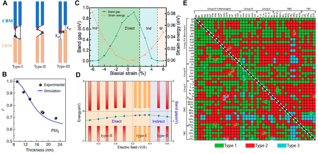
FIGURE 1. (A) Schematic illustration of heterojunctions with type-I, type-II, and type-III band alignments. (B) Thickness-dependent spin polarization in PbI2/WS2 heterojunctions. The blue line represents the numerical simulation result (Yuan et al., 2018). (C) Bandgap of the Sb/AlAs heterojunctions vary with the biaxial strain. Positive and negative numbers represent tensile and compressive strains, respectively (Jia et al., 2021). (D) Bandgap and band edge location of Janus-In2STe/InSe vdWH with various electric fields (Li et al., 2020a). (E) Periodic table of heterostructures (Özçelik et al., 2016).
Nowadays, vdWHs with different band alignments are constructed, and the resulting devices are gradually becoming the alternative to the widely used silicon-based devices. As a result, many approaches to modulate the band alignment in heterojunctions have evolved. Here, we mainly introduce these approaches and the application of vdWHs in photoelectric and electronic devices.
2 Band Alignment Engineering
Band alignment engineering governs the charge transport behavior in heterojunctions, so it is an efficient way to regulate the photoelectric and electrical properties through bandgap edge adjustment. There are many ways to regulate the band arrangement, such as composition modulation, component thickness, strain, and electric field.
Integrated by two (or more) kinds of semiconductors, the properties of heterojunctions are greatly influenced by the components, especially for the vdW layered heterojunctions composed of 2D dangling bond free surface layers (Liu et al., 2020a; Hou et al., 2020; Lee et al., 2020; Zhang et al., 2020). So, one of the most straightforward ways to get a heterojunction with the desired performance is to combine different semiconductors with diverse properties. Theoretically, dozens of 2D layer materials and their combinations of heterojunctions are explored (Özçelik et al., 2016). As shown in Figures 1A,E, a detailed list of heterojunctions is constructed. Type-I, type-II, and type-III band alignments are achieved through different combinations; therefore, the periodic table provides a useful guidance for future research.
Transition metal dichalcogenides (TMDs) are the most widely used 2D semiconductors, and the heterojunctions based on TMDs covered the three types of band arrangements. Type-II band alignment is common in TMD heterojunctions; furthermore, the type-II band alignment in vertically stacked TMD heterojunctions effectively facilitates photogenerated carrier separation and inhibits electron–hole recombination (Hong et al., 2014; Ji et al., 2017). In contrast to the strong covalent bonding within the layer, the interlaminar interactions are mainly vdW forces in the range of physical adsorption, which allows monolayer exfoliation and the layer-dependent features (Liu et al., 2020b; Chen et al., 2020). Lu et al. combined the most common TMDs, MoS2 and the other MX2, to 2D MoS2/MX2 vdWHs and found that for vdWHs with MoS2 and MoSe2, CrS2, CrSe2, and WS2 showed type-II features with an indirect bandgap while WSe2/MoS2 vdWHs kept the direct bandgap of the MoS2 layer (Lu et al., 2014).
The heterojunction that is a combination of TMDs and zinc oxide (ZnO) has attracted much interest among researchers in recent years (Ta et al., 2016). The ZnO has the same geometrical structure as graphene; like other layered materials, the bandgap is sensitive to the thickness while the bandgap of monolayer ZnO is 3.3 eV (Topsakal et al., 2009). Therefore, the bandgap of ZnO tends to significantly narrow through the formation of heterojunctions. For example, in 2H-TiS2/ZnO vdWHs, the heterojunction appears as a narrow indirect bandgap of 0.34 eV with the formation of type-II band alignment; meanwhile a large potential drop (3.75 eV) and band offset are formed which improve charge separation efficiency and then make the heterojunction desirable for optoelectronic applications (Rahimi, 2021). In MoS2/ZnO vdWHs, a type-II band alignment is formed with a large built-in electric field. These characters ensure that the heterojunction exhibits good optical absorption ability in the visible region and then potentially be used in photoelectric and photocatalytic devices (Wang et al., 2018a).
The type I band alignment based on semiconducting TMDs shows great application potential in photonic and photoelectric devices with ultrafast (∼100 fs) interface response and charge transfer velocity (Wu et al., 2019; Li et al., 2020b). The MoTe2/WS2 vdWH shows type-I band alignment and the excitons are confined in the low-bandgap MoTe2 layer; therefore, the exciton absorption of the WS2 is bleached in the adjacent MoTe2 layer (Li et al., 2021). Similarly, the bandgap edge of type-I band alignment in Sb/PtTe2 heterojunctions is contributed by the CBM and VBM of PtTe2, which also makes efficient recombination of photoexcited carriers because of confining electrons irradiated by light (Shokri and Yazdani, 2021).
Currently, both type-I and type-II band alignment are common in vdWHs, while few systems show type-III images. Type-III heterojunctions, as previously mentioned, have a broken bandgap, which is appropriate for tunneling field effect transistors (Yan et al., 2017). TMDs are still outstanding in the application of type-III band arrangement. The MX2/MoS2 heterojunctions, with M = Fe, V; X = S, Se, exhibit metallic characters with type-III band alignment (Lu et al., 2014). Also, the WTe2/HfS2 vdWH shows a type-III band alignment, which is confirmed by XPS and UV–V (Lei et al., 2019).
In addition to TMDs, other vdW layered semiconductors have been developed rapidly in the field of heterojunctions. For instance, the heterojunction composed of the metal monochalcogenides InSe and GeSe and Xenes arsenene. The InSe/GeSe vdWH shows a band alignment with a near-zero bandgap which can simplify the reversing circuit and speed regulating circuit; therefore, the field effect transistor (FET) based on the InSe/GeSe vdW heterojunction is suitable for constructing as a gate-controllable half-wave rectifier (Yan et al., 2021). The stable InS/arsenene vdWH possesses excellent flexibility and high carrier mobility, and what is more, a stable type-II band alignment is formed within the regulation of the vertical strain (Yao et al., 2021). Recently, the monolayer Janus TMD MXY has gotten a lot of attention for its broken mirror symmetry, which adds another dimension of regulation (Li et al., 2017). Stacking Janus monolayers into vdWHs have unlocked even more excellent properties (He et al., 2020). Rawat et al. systematically studied the vdWHs composed of Janus MXY (M represents Mo, W, Hf, Zr; X, Y represents S, Se, Te; and X is different from Y) (Rawat et al., 2020). The Janus MXY form 19 type-II vdWHs, and the energy conversion efficiency of five of the vdWHs is up to 15–20% (Rawat et al., 2020).
For 2D type-II heterojunctions, it is critical for the conduction and valence band edges to be momentum-matched (Özçelik et al., 2016), which will promote the efficiency of photon excited electron–hole pairs (Wang et al., 2020b). The BP/BSe vdWH is proven to be thermodynamic and kinetically stable at room temperature, and the momentum-matched type-II band alignment is achieved with electron transfer from BSe to BP (Pham et al., 2020). However, due to a natural lattice mismatch, most type-II semiconductor heterojunctions are momentum–space mismatch. To solve the intractable problem, a universal approach is proposed through using metal-supported homojunctions, and furthermore, the momentum–space match can be in a wide K-range but not a special K-point only, through a band-nesting effect in degenerately doped 2D multilayered semiconductor homojunctions induced by metal supporting (Wang et al., 2020b).
Due to the quantum confinement effect, the electronic band structure, polarization, and optical properties of layered materials can be easily affected by the thickness (Cai et al., 2014; Hamer et al., 2019). For example, the bandgap gradually widens as the number of layers decreases in most TMDs (e.g., the bandgap of MoS2 decreases as the number of layers increases (Ellis et al., 2011; Rahimi, 2021)) and black phosphorus (Ellis et al., 2011; Tongay et al., 2012; Fuh et al., 2016; Jiang et al., 2018; Zhong et al., 2018). This suggests a possible approach to construct functional heterojunctions through thickness engineering (Rahimi, 2021). Similarly, the light emission in 2D TMDs changes observably with the layer number and stacking sequence (Palummo et al., 2015). The radiative recombination in bilayer MoS2 is slower than in the monolayers, which is up to a few picoseconds at low temperature. Especially, the interlayer excitons in MoS2/WS2 and MoSe2/WSe2 vdWHs lived very long (∼20–30 ns at room temperature) since the constituted electrons and holes localized at different layers (Palummo et al., 2015). The carrier lifetime can be manipulated by layer thickness in vdW heterojunctions of type-I PbI2/WS2 and type-II PbI2/WSe2 band alignments. Similar to PbI2, the carrier lifetime of PbI2/WS2 heterojunctions increases with increasing thickness, which causes the decrease in the circular polarization. Besides, the polarization for the PbI2 from the PbI2/WS2 heterojunction decreases from 0.998 to 0.693 as the heterojunction thickness increases from 9.2 to 22.6 nm (Yamaoka et al., 2018; Zhang et al., 2020) as displayed in Figure 1B.
Semiconductor thickness can also control the carrier migration. That is, the performance of metal–2D semiconductor junctions, especially the interface barrier which represents the barrier to be crossed for carrier migration, is thickness-dependent. The Fermi-level pinning factor of metal–2D multilayered semiconductor junctions depends sensitively on the layer number of few-layer 2D semiconductors (Wang et al., 2020a; Wang et al., 2020c).
The ultrathin character allows the electronic properties of 2D materials to be tuned by external electric fields, which provides a feasible method for band arrangement in 2D heterojunctions (Wang et al., 2018b; Rahimi, 2021). Based on the capacitance model, when the gate voltage is applied, the doping concentration and even the conductive -in materials will be adjusted in the way of electrostatic doping (Pan et al., 2020; Sun et al., 2020; Rahimi, 2021). In this way, the band offset between semiconductors can be designed dynamically (Rahimi, 2021). Through the vertical electric field, a transition of band alignment from type-III to type-II is observed in WTe2/HfS2 vdW heterojunctions (Lei et al., 2019), a type-II to a type-I transformation is realized in SnS2/WSe2 bilayer heterojunctions (Guan et al., 2021), and a transformation from type-I to type-II band alignment is implemented in Sb/PtTe2 vdW heterojunctions (Shokri and Yazdani, 2021). The electric field can also change the band edge and bandgap. For SnS2/WSe2, the bandgap decreases monotonically with the increasing electric field, and when the electric field reaches above 0.3 V/Å, the heterojunction transforms to a conductor (Guan et al., 2021).
Due to the existence of the internal electric field, the Janus heterojunction shows different characteristics under the action of the external electric field. In Janus-In2STe/InSe vdWHs, both strain and the electric field can cause direct–indirect band structure transformation and staggered-straddling band alignment (Li et al., 2020a). In addition, the variation trend of the bandgap is related not only to electric field intensity but also to electric field direction (Li et al., 2020a). As shown in Figure 1D, the bandgap of type-I In2STe/InSe vdWHs first increases to the peak value of 1.32 eV with a positive electric field and then the bandgap reduces with a larger electric field, while the band alignment turns to type-II. When a negative electric field is applied, the heterojunction keeps the property of staggered band alignment (Li et al., 2020a).
As stated above, the novel strategy of the external electric field plays an important role in modulating electronic characteristics for vdW heterojunctions. Strain, including vertical and biaxial, often discussed together with the electric field, is also an effective method to regulate the electric properties such as conductivity and transportability of low-dimensional semiconductor systems (Sun et al., 2017).
Especially, the biaxial strain engineering is effective in modulating the bandgaps of 2D heterojunctions (Lei et al., 2019; Zribi et al., 2019; Guan et al., 2021). As shown in Figure 1C, the bandgap of the Sb/AlAs heterojunctions has a peak value of 0.909 eV at 1% tensile strain, and the heterojunction turns to metal at 6% tensile strain (Jia et al., 2021). Guo et al. investigated the regulation of strain on MoSSe/WSSe vdWHs (Guo et al., 2020), and they found that strain can effectually control the bandgap of vdWHs, and a large tensile strain can even turn semiconductors to metal. With biaxial tensile strain, the bandgap of MX2/MoS2 (MoSe2, CrS2, CrSe2, WS2, and WSe2) bilayer heterojunctions experience a semiconductor-to-metal transition; while for WSe2/MoS2 heterojunctions, an indirect bandgap is achieved from a direct one (Lu et al., 2014).
For 2D heterojunctions, tensile strain also provides an approach to enhance light absorption and improve solar energy conversion efficiency. As in SnS2/WSe2 heterojunctions, with compressive strain exceeding –9%, the indirect type-II semiconductor will transform to a type-I semiconductor which provides theoretical basis for future practical application (Guan et al., 2021). Similarly, the band alignment of WTe2/HfS2 vdW heterojunctions transforms from type-III to type-II with biaxial strain, which is because the position of high symmetry points of the band edge changes with strain (Lei et al., 2019).
3 Application in Optoelectronic and Electronic Devices
VdWHs, with their on-demand design capabilities, offer amazing opportunities to build new types of electronic and optoelectronic devices (Liu et al., 2020b). Especially, 2D semiconductors and heterojunctions exhibit outstanding properties, such as novel interlayer interaction (Li et al., 2020c; Li et al., 2020d; Reddy et al., 2020; Sung et al., 2020), high on/off ratio, and fast transit time (Deng et al., 2014) of current at room temperature, which make them backbones for solid-state–based atomically thin optoelectronic and electronic devices.
In type-II band arrangement vdWHs, photo-induced electrons and holes tend to move in opposite directions, resulting in high separation efficiency of charge carriers, which provides novel exciton devices with large binding energy (Furchi et al., 2014; Ross et al., 2017). As shown in Figure 2A, in MoSe2/WSe2 heterojunctions, the resulting photocurrent of the interlayer exciton is 200 times less than the amplitude of the intralayer exciton’s resonance excitation, which means that the sandwich exciton’s vibrator strength is hundreds of orders less than the intralayer exciton due to the opposite spatial separation of the electron and hole layers (Ross et al., 2017).
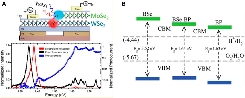
FIGURE 2. (A) MoSe2−WSe2 vdWH used in interlayer exciton optoelectronics (Ross et al., 2017). (B) Photocatalytic performance of isolated BP and BSe monolayers and BP–BSe vdWH (Pham et al., 2020).
Hydrogen is a secondary source of energy which can be obtained from other major energy sources (Veziroglu, 2007; Pham et al., 2020). For its low emission, environmental protection, and more sustainable energy system characters (Balat, 2008; Pham et al., 2020), hydrogen becomes strategically important. Recently, semiconductors and their heterojunctions have been used as major photocatalysts for converting sunlight to hydrogen because of their chemical and photochemical stability, as well as effective visible light absorption capacity because of suitable band arrangement and band structure (Osterloh, 2008; Axet et al., 2019; Pham et al., 2020). As shown in Figure 2B, the band edges of BP-BSe heterojunctions have reached an energetically favorable position and crossed the redox potential, which is suitable for water decomposition at pH = 0 (Pham et al., 2020). In addition, the bandgap value of the vdWH is larger than the lowest energy (1.23 eV) needed for the photocatalysis reactions, which is beneficial to a highly efficient photocatalyst for converting water into hydrogen and the production of clean and renewable energy equipment applications.
These results establish the foundation for utilizing the interlayer exciton and photocatalysis in future 2D heterojunction optoelectronic devices. Simultaneously, the 2D materials are promising for future two-terminal devices, transistors, and memories because of their surface dangling free bonds, atomically thin body, atomically sharp heterojunctions, and band alignments through the modulating method described above. For example, heterojunctions with type-III band alignment can actuate Esaki diodes with significant negative differential resistance, heterojunctions with p–n junctions enable vertical TFETs with an ultra-steep subthreshold slope, and the atomically thin body supplies 2D heterojunction transistors with strong immunity against short-channel effects. In electronic devices, the high contact resistance is an obstacle to realizing the potential of these materials for low-power applications. MoS2 is the outstanding representative of two-dimensional semiconductors, and the reported contact resistance of metal−MoS2 is 10 times higher than that of Si (Kang et al., 2014). The Gr/h-BN/Gr vdW heterostructure is the first reported tunneling field-effect transistor (Britnell et al., 2012), and by replacing h-BN with 2D WS2, the low tunneling current density (pA μm−2) and on/off ratio (around 50) can be improved to μA μm−2 and 106, respectively (Lopez-Sanchez et al., 2013). In addition, 2D materials can maintain their sharp band edges even at atomic thickness. This excellent property can be used to create vertical p–n junction devices (Lee et al., 2014), such as SnS2/WSe2 (Guan et al., 2021), MoS2/WS2 (Ji et al., 2017), and MoSSe/WSSe (Guo et al., 2020) as discussed before, which are on account of the mechanism of band-to-band tunneling.
However, there are many challenges and limitations in 2D optoelectronic and electronic devices, such as high-quality large-scale synthesis and large contact resistances. Further research and efforts are needed before the actual applications (Zhu et al., 2019).
4 Conclusion and Perspectives
In summary, this article provides a brief review of 2D layered materials and their vdWHs based on band alignment engineering and their applications in optoelectronic and electronic devices. In the first, three types of band alignments and their carrier transport characteristics at interfaces are introduced. Subsequently, band alignment regulation and control methods are listed, including composition modulation, layer thickness adjustment, strain, and electric field. Finally, optoelectronic and electronic devices based on 2D heterojunctions are summarized.
Although 2D layered materials have many attractive properties and advantages, there are still many problems to be overcome before their applications in reality, such as the preparation of large size and high-quality 2D materials and 2D heterojunctions. What is more, high interfacial resistance is also holding it back. Much research and development efforts should be input before 2D semiconductor devices will be ready for mainstream applications. In a word, 2D semiconductors and their heterojunctions would be a hot topic in future research and can potentially have broad applications.
Author Contributions
All authors listed have made a substantial, direct, and intellectual contribution to the work and approved it for publication.
Funding
This work was financially supported by the Natural Science Foundation of Hubei Province of China (No. 2020CFB245); Teaching Research Projects in Colleges and Universities of Hubei (No. 2020668); and Hubei Province Education Department Scientific Research Plan Guiding Project (No. B2021260).
Conflict of Interest
The authors declare that the research was conducted in the absence of any commercial or financial relationships that could be construed as a potential conflict of interest.
Publisher’s Note
All claims expressed in this article are solely those of the authors and do not necessarily represent those of their affiliated organizations, or those of the publisher, the editors, and the reviewers. Any product that may be evaluated in this article, or claim that may be made by its manufacturer, is not guaranteed or endorsed by the publisher.
Supplementary Material
The Supplementary Material for this article can be found online at: https://www.frontiersin.org/articles/10.3389/fenrg.2021.802055/full#supplementary-material
References
Autere, A., Jussila, H., Dai, Y., Wang, Y., Lipsanen, H., and Sun, Z. (2018). Nonlinear Optics with 2D Layered Materials. Adv. Mater. 30, 1705963. doi:10.1002/adma.201705963
Axet, M. R., Durand, J., Gouygou, M., and Serp, P. (2019). “Surface Coordination Chemistry on Graphene and Two-Dimensional Carbon Materials for Well-Defined Single Atom Supported Catalysts,” in Advances in Organometallic Chemistry. Editor P.J. Pérez (Cambridge: Academic Press), 53–174. doi:10.1016/bs.adomc.2019.01.002
Balat, M. (2008). Potential Importance of Hydrogen as a Future Solution to Environmental and Transportation Problems. Int. J. Hydrogen Energ. 33, 4013–4029. doi:10.1016/j.ijhydene.2008.05.047
Britnell, L., Gorbachev, R. V., Jalil, R., Belle, B. D., Schedin, F., Mishchenko, A., et al. (2012). Field-Effect Tunneling Transistor Based on Vertical Graphene Heterostructures. Science 335, 947–950. doi:10.1126/science.1218461
Butler, S. Z., Hollen, S. M., Cao, L., Cui, Y., Gupta, J. A., Gutiérrez, H. R., et al. (2013). Progress, Challenges, and Opportunities in Two-Dimensional Materials beyond Graphene. ACS Nano 7, 2898–2926. doi:10.1021/nn400280c
Cai, Y., Zhang, G., and Zhang, Y.-W. (2014). Layer-dependent Band Alignment and Work Function of Few-Layer Phosphorene. Sci. Rep. 4, 6677. doi:10.1038/srep06677
Cao, S., Xing, Y., Han, J., Luo, X., Lv, W., Lv, W., et al. (2018). Ultrahigh-photoresponsive UV Photodetector Based on a BP/ReS2 Heterostructure P-N Diode. Nanoscale 10, 16805–16811. doi:10.1039/c8nr05291c
Chaves, A., Azadani, J. G., Alsalman, H., da Costa, D. R., Frisenda, R., Chaves, A. J., et al. (2020). Bandgap Engineering of Two-Dimensional Semiconductor Materials. Npj 2d Mater. Appl. 4, 29. doi:10.1038/s41699-020-00162-4
Chen, E., Xu, W., Chen, J., and Warner, J. H. (2020). 2D Layered noble Metal Dichalcogenides (Pt, Pd, Se, S) for Electronics and Energy Applications. Mater. Today Adv. 7, 100076. doi:10.1016/j.mtadv.2020.100076
Deng, Y., Luo, Z., Conrad, N. J., Liu, H., Gong, Y., Najmaei, S., et al. (2014). Black Phosphorus-Monolayer MoS2 van der Waals Heterojunction p-n Diode. ACS Nano 8, 8292–8299. doi:10.1021/nn5027388
Ellis, J. K., Lucero, M. J., and Scuseria, G. E. (2011). The Indirect to Direct Band gap Transition in Multilayered MoS2 as Predicted by Screened Hybrid Density Functional Theory. Appl. Phys. Lett. 99, 261908. doi:10.1063/1.3672219
Fuh, H.-R., Yan, B., Wu, S.-C., Felser, C., and Chang, C.-R. (2016). Metal-insulator Transition and the Anomalous Hall Effect in the Layered Magnetic Materials VS2 and VSe2. New J. Phys. 18, 113038. doi:10.1088/1367-2630/18/11/113038
Furchi, M. M., Pospischil, A., Libisch, F., Burgdörfer, J., and Mueller, T. (2014). Photovoltaic Effect in an Electrically Tunable van der Waals Heterojunction. Nano Lett. 14, 4785–4791. doi:10.1021/nl501962c
Geim, A. K., and Grigorieva, I. V. (2013). Van der Waals heterostructures. Nature 499, 419–425. doi:10.1038/nature12385
Guan, Y., Li, X., Hu, T., Zhang, N., Niu, R., and Liu, Z. (2021). Tunable Electronic Properties of SnS2/WSe2 Hetero-Structure: A Frist Principle Study. Superlattices And Microstructures 150, 106806. doi:10.1016/j.spmi.2021.106806
Guo, W., Ge, X., Sun, S., Xie, Y., and Ye, X. (2020). The strain effect on the electronic properties of the MoSSe/WSSe van der Waals heterostructure: a first-principles study. Phys. Chem. Chem. Phys. 22, 4946–4956. doi:10.1039/D0CP00403K
Hamer, M. J., Zultak, J., Tyurnina, A. V., Zólyomi, V., Terry, D., Barinov, A., et al. (2019). Indirect to Direct Gap Crossover in Two-Dimensional InSe Revealed by Angle-Resolved Photoemission Spectroscopy. ACS Nano 13, 2136–2142. doi:10.1021/acsnano.8b08726
He, C., Han, F. S., Zhang, J. H., and Zhang, W. X. (2020). The In2SeS/g-C3N4heterostructure: a New Two-Dimensional Material for Photocatalytic Water Splitting. J. Mater. Chem. C 8, 6923–6930. doi:10.1039/D0TC00852D
Hong, X., Kim, J., Shi, S.-F., Zhang, Y., Jin, C., Sun, Y., et al. (2014). Ultrafast Charge Transfer in Atomically Thin MoS2/WS2 Heterostructures. Nat. Nanotech 9, 682–686. doi:10.1038/nnano.2014.167
Hou, X., Liu, C., Ding, Y., Liu, L., Wang, S., and Zhou, P. (2020). A Logic‐Memory Transistor with the Integration of Visible Information Sensing‐Memory‐Processing. Adv. Sci. 7, 2002072. doi:10.1002/advs.202002072
Ji, Z., Hong, H., Zhang, J., Zhang, Q., Huang, W., Cao, T., et al. (2017). Robust Stacking-independent Ultrafast Charge Transfer in MoS2/WS2 Bilayers. ACS Nano 11, 12020–12026. doi:10.1021/acsnano.7b04541
Jia, Y., Wei, X., Zhang, Z., Liu, J., Tian, Y., Zhang, Y., et al. (2021). A Theoretical Design of Photodetectors Based on Two-Dimensional Sb/AlAs Type-II Heterostructures. Crystengcomm 23, 1033–1042. doi:10.1039/d0ce01633k
Jiang, B., Zou, X., Su, J., Liang, J., Wang, J., Liu, H., et al. (2018). Impact of Thickness on Contact Issues for Pinning Effect in Black Phosphorus Field-Effect Transistors. Adv. Funct. Mater. 28, 1801398. doi:10.1002/adfm.201801398
Kahn, E., Liu, M., Zhang, T., Liu, H., Fujisawa, K., Bepete, G., et al. (2020). Functional Hetero-Interfaces in Atomically Thin Materials. Mater. Today 37, 74–92. doi:10.1016/j.mattod.2020.02.021
Kang, J., Liu, W., Sarkar, D., Jena, D., and Banerjee, K. (2014). Computational Study of Metal Contacts to Monolayer Transition-Metal Dichalcogenide Semiconductors. Phys. Rev. X 4, 4031005. doi:10.1103/PhysRevX.4.031005
Kunstmann, J., Mooshammer, F., Nagler, P., Chaves, A., Stein, F., Paradiso, N., et al. (2018). Momentum-space indirect interlayer excitons in transition-metal dichalcogenide van der Waals heterostructures. Nat. Phys 14, 801–805. doi:10.1038/s41567-018-0123-y
Lee, C.-H., Lee, G.-H., van der Zande, A. M., Chen, W., Li, Y., Han, M., et al. (2014). Atomically thin p-n junctions with van der Waals heterointerfaces. Nat. Nanotech 9, 676–681. doi:10.1038/nnano.2014.150
Lee, S.-J., Lin, Z., Huang, J., Choi, C. S., Chen, P., Liu, Y., et al. (2020). Programmable Devices Based on Reversible Solid-State Doping of Two-Dimensional Semiconductors with Superionic Silver Iodide. Nat. Electron. 3, 630–637. doi:10.1038/s41928-020-00472-x
Lei, C., Ma, Y., Xu, X., Zhang, T., Huang, B., and Dai, Y. (2019). Broken-Gap Type-III Band Alignment in WTe2/HfS2 van der Waals Heterostructure. J. Phys. Chem. C 123, 23089–23095. doi:10.1021/acs.jpcc.9b07862
Li, F., Wei, W., Zhao, P., Huang, B., and Dai, Y. (2017). Electronic and Optical Properties of Pristine and Vertical and Lateral Heterostructures of Janus MoSSe and WSSe. J. Phys. Chem. Lett. 8, 5959–5965. doi:10.1021/acs.jpclett.7b02841
Li, S.-Y., Su, Y., Ren, Y.-N., and He, L. (2020). Valley Polarization and Inversion in Strained Graphene via Pseudo-landau Levels, Valley Splitting of Real Landau Levels, and Confined States. Phys. Rev. Lett. 124, 106802. doi:10.1103/PhysRevLett.124.106802
Li, W., Lu, X., Dubey, S., Devenica, L., and Srivastava, A. (2020). Dipolar interactions between localized interlayer excitons in van der Waals heterostructures. Nat. Mater. 19, 624–629. doi:10.1038/s41563-020-0661-4
Li, X., Zhai, B., Song, X., Yan, Y., Li, J., and Xia, C. (2020). Two-dimensional Janus-In2STe/InSe Heterostructure with Direct gap and Staggered Band Alignment. Appl. Surf. Sci. 509, 145317. doi:10.1016/j.apsusc.2020.145317
Li, Y., Chen, Y., Zhou, H., and Zhu, H. (2021). Transient Optical Modulation of Two-Dimensional Materials by Excitons at Ultimate Proximity. ACS Nano 15, 5495–5501. doi:10.1021/acsnano.1c00243
Li, Y., Zhou, H., Chen, Y., Zhao, Y., and Zhu, H. (2020). Efficient Hot-Electron Extraction in Two-Dimensional Semiconductor Heterostructures by Ultrafast Resonant Transfer. J. Chem. Phys. 153, 044705. doi:10.1063/5.0018072
Liu, B., Du, J., Yu, H., Hong, M., Kang, Z., Zhang, Z., et al. (2020). The coupling effect characterization for van der Waals structures based on transition metal dichalcogenides. Nano Res. 14, 1734–1751. doi:10.1007/s12274-020-3253-3
Liu, C., Chen, H., Wang, S., Liu, Q., Jiang, Y.-G., Zhang, D. W., et al. (2020). Two-dimensional Materials for Next-Generation Computing Technologies. Nat. Nanotechnol. 15, 545–557. doi:10.1038/s41565-020-0724-3
Lopez-Sanchez, O., Lembke, D., Kayci, M., Radenovic, A., and Kis, A. (2013). Ultrasensitive Photodetectors Based on Monolayer MoS2. Nat. Nanotech 8, 497–501. doi:10.1038/nnano.2013.100
Lu, N., Guo, H., Li, L., Dai, J., Wang, L., Mei, W.-N., et al. (2014). MoS2/MX2 Heterobilayers: Bandgap Engineering via Tensile Strain or External Electrical Field. Nanoscale 6, 2879–2886. doi:10.1039/C3NR06072A
Lukman, S., Ding, L., Xu, L., Tao, Y., Riis-Jensen, A. C., Zhang, G., et al. (2020). High Oscillator Strength Interlayer Excitons in Two-Dimensional Heterostructures for Mid-infrared Photodetection. Nat. Nanotechnol. 15, 675–682. doi:10.1038/s41565-020-0717-2
Mak, K. F., Lee, C., Hone, J., Shan, J., and Heinz, T. F. (2010). Atomically ThinMoS2: A New Direct-Gap Semiconductor. Phys. Rev. Lett. 105, 136805. doi:10.1103/PhysRevLett.105.136805
Novoselov, K. S., Fal′ko, V. I., Colombo, L., Gellert, P. R., Schwab, M. G., and Kim, K. (2012). A Roadmap for Graphene. Nature 490, 192–200. doi:10.1038/nature11458
Osterloh, F. E. (2008). Inorganic Materials as Catalysts for Photochemical Splitting of Water. Chem. Mater. 20, 35–54. doi:10.1021/cm7024203
Özçelik, V. O., Azadani, J. G., Yang, C., Koester, S. J., and Low, T. (2016). Band Alignment of Two-Dimensional Semiconductors for Designing Heterostructures with Momentum Space Matching. Phys. Rev. B 94, 035125. doi:10.1103/PhysRevB.94.035125
Palummo, M., Bernardi, M., and Grossman, J. C. (2015). Exciton Radiative Lifetimes in Two-Dimensional Transition Metal Dichalcogenides. Nano Lett. 15, 2794–2800. doi:10.1021/nl503799t
Pan, C., Wang, C.-Y., Liang, S.-J., Wang, Y., Cao, T., Wang, P., et al. (2020). Reconfigurable Logic and Neuromorphic Circuits Based on Electrically Tunable Two-Dimensional Homojunctions. Nat. Electron. 3, 383–390. doi:10.1002/adfm.20190964510.1038/s41928-020-0433-9
Pham, K. D., Tan, L. V., Idrees, M., Amin, B., Hieu, N. N., Phuc, H. V., et al. (2020). Electronic structures, and optical and photocatalytic properties of the BP-BSe van der Waals heterostructures. New J. Chem. 44, 14964–14969. doi:10.1039/d0nj03236k
Rahimi, K. (2021). Electric-field- and Strain-Induced Adjustability of vdW Heterostructure of G-ZnO/2H-TiS2 for Optoelectronic Applications. Mater. Lett. 282, 128680. doi:10.1016/j.matlet.2020.128680
Rawat, A., Mohanta, M. K., Jena, N., Dimple, , Ahammed, R., and De Sarkar, A. (2020). Nanoscale Interfaces of Janus Monolayers of Transition Metal Dichalcogenides for 2D Photovoltaic and Piezoelectric Applications. J. Phys. Chem. C 124, 10385–10397. doi:10.1021/acs.jpcc.0c02199
Reddy, B. A., Ponomarev, E., Gutiérrez-Lezama, I., Ubrig, N., Barreteau, C., Giannini, E., et al. (2020). Synthetic Semimetals with van der Waals Interfaces. Nano Lett. 20, 1322–1328. doi:10.1021/acs.nanolett.9b04810
Ross, J. S., Rivera, P., Schaibley, J., Lee-Wong, E., Yu, H., Taniguchi, T., et al. (2017). Interlayer Exciton Optoelectronics in a 2D Heterostructure P-N Junction. Nano Lett. 17, 638–643. doi:10.1021/acs.nanolett.6b03398
Shokri, A., and Yazdani, A. (2021). Band alignment engineering, electronic and optical properties of Sb/PtTe2 van der Waals heterostructure: effects of electric field and biaxial strain. J. Mater. Sci. 56, 5658–5669. doi:10.1007/s10853-020-05561-y
Sun, X., Zhu, C., Liu, H., Zheng, B., Liu, Y., Yi, J., et al. (2020). Contact and Injection Engineering for Low SS Reconfigurable FETs and High Gain Complementary Inverters. Sci. Bull. 65, 2007–2013. doi:10.1016/j.scib.2020.06.033
Sun, X., Zhu, C., Zhu, X., Yi, J., Liu, Y., Li, D., et al. (2021). Recent Advances in Two‐Dimensional Heterostructures: From Band Alignment Engineering to Advanced Optoelectronic Applications. Adv. Electron. Mater. 7, 2001174. doi:10.1002/aelm.202001174
Sun, Y., Wang, R., and Liu, K. (2017). Substrate Induced Changes in Atomically Thin 2-dimensional Semiconductors: Fundamentals, Engineering, and Applications. Appl. Phys. Rev. 4, 011301. doi:10.1063/1.4974072
Sung, J., Zhou, Y., Scuri, G., Zólyomi, V., Andersen, T. I., Yoo, H., et al. (2020). Broken Mirror Symmetry in Excitonic Response of Reconstructed Domains in Twisted MoSe2/MoSe2 Bilayers. Nat. Nanotechnol. 15, 750–754. doi:10.1038/s41565-020-0728-z
Ta, H., Zhao, L., Pohl, D., Pang, J., Trzebicka, B., Rellinghaus, B., et al. (2016). Graphene-Like ZnO: A Mini Review. Crystals 6 (8), 100. doi:10.3390/cryst6080100
Tongay, S., Zhou, J., Ataca, C., Lo, K., Matthews, T. S., Li, J., et al. (2012). Thermally Driven Crossover from Indirect toward Direct Bandgap in 2D Semiconductors: MoSe2 versus MoS2. Nano Lett. 12, 5576–5580. doi:10.1021/nl302584w
Topsakal, M., Cahangirov, S., Bekaroglu, E., and Ciraci, S. (2009). First-principles Study of Zinc Oxide Honeycomb Structures. Phys. Rev. B 80, 235119. doi:10.1103/PhysRevB.80.235119
Veziroglu, T. N. (2007). 21st Century's Energy: Hydrogen Energy System. Dordrecht: Springer Netherlands, 9–31. doi:10.1007/978-1-4020-6442-5_2
Wang, C., Peng, L., Qian, Q., Du, J., Wang, S., and Huang, Y. (2018). Tuning the Carrier Confinement in GeS/Phosphorene van der Waals Heterostructures. Small 14, 1703536. doi:10.1002/smll.201703536
Wang, Q., Dou, K., and Shi, X. (2020). Band Alignment in Multilayered Semiconductor Homojunctions Supported on Metals. J. Mater. Chem. C 8, 959–967. doi:10.1039/C9TC04512K
Wang, Q. H., Kalantar-Zadeh, K., Kis, A., Coleman, J. N., and Strano, M. S. (2012). Electronics and Optoelectronics of Two-Dimensional Transition Metal Dichalcogenides. Nat. Nanotech 7, 699–712. doi:10.1038/nnano.2012.193
Wang, Q., Shao, Y., Gong, P., and Shi, X. (2020). Metal-2D Multilayered Semiconductor Junctions: Layer-Number Dependent Fermi-Level Pinning. J. Mater. Chem. C 8, 3113–3119. doi:10.1039/C9TC06331E
Wang, Q., Shao, Y., and Shi, X. (2020). Mechanism of Charge Redistribution at the Metal-Semiconductor and Semiconductor-Semiconductor Interfaces of Metal-Bilayer MoS2 Junctions. J. Chem. Phys. 152, 244701. doi:10.1021/acsnano.0c0866810.1063/5.0010849
Wang, S., Ren, C., Tian, H., Yu, J., and Sun, M. (2018). MoS2/ZnO van der Waals heterostructure as a high-efficiency water splitting photocatalyst: a first-principles study. Phys. Chem. Chem. Phys. 20, 13394–13399. doi:10.1039/c8cp00808f
Wu, L., Chen, Y., Zhou, H., and Zhu, H. (2019). Ultrafast Energy Transfer of Both Bright and Dark Excitons in 2D van der Waals Heterostructures Beyond Dipolar Coupling. ACS Nano 13, 2341–2348. doi:10.1021/acsnano.8b09059
Xiong, X., Kang, J., Hu, Q., Gu, C., Gao, T., Li, X., et al. (2020). Reconfigurable Logic‐in‐Memory and Multilingual Artificial Synapses Based on 2D Heterostructures. Adv. Funct. Mater. 30, 1909645. doi:10.1002/adfm.201909645
Yamaoka, T., Lim, H. E., Koirala, S., Wang, X., Shinokita, K., Maruyama, M., et al. (2018). Efficient Photocarrier Transfer and Effective Photoluminescence Enhancement in Type I Monolayer MoTe2/WSe2 Heterostructure. Adv. Funct. Mater. 28, 1801021. doi:10.1002/adfm.201801021
Yan, X., Liu, C., Li, C., Bao, W., Ding, S., Zhang, D. W., et al. (2017). Tunable SnSe2/WSe2 Heterostructure Tunneling Field Effect Transistor. Small 13, 1701478. doi:10.1002/smll.201701478
Yan, Y., Li, S., Du, J., Yang, H., Wang, X., Song, X., et al. (2021). Reversible Half Wave Rectifier Based on 2D InSe/GeSe Heterostructure with Near‐Broken Band Alignment. Adv. Sci. 8 (4), 1903252. doi:10.1002/advs.201903252
Yao, H., Zhang, C., Wang, Q., Li, J., Yu, Y., Xu†, F., et al. (2021). Tunable Electronic Properties and Band Alignments of InS-Arsenene Heterostructures via External Strain and Electric Field. New J. Chem. 45, 2508–2519. doi:10.1039/d0nj05787h
Yuan, L., Chung, T.-F., Kuc, A., Wan, Y., Xu, Y., Chen, Y. P., et al. (2018). Photocarrier Generation from Interlayer Charge-Transfer Transitions in WS 2 -graphene Heterostructures. Sci. Adv. 4 (2), 1700324. doi:10.1126/sciadv.1700324
Zahid, F., Liu, L., Zhu, Y., Wang, J., and Guo, H. (2013). A Generic Tight-Binding Model for Monolayer, Bilayer and Bulk MoS2. Aip Adv. 3 (5), 052111. doi:10.1063/1.4804936
Zhang, D., Liu, Y., He, M., Zhang, A., Chen, S., Tong, Q., et al. (2020). Room temperature near unity spin polarization in 2D Van der Waals heterostructures. Nat. Commun. 11, 442. doi:10.1038/s41467-020-18307-w
Zhong, M., Xia, Q., Pan, L., Liu, Y., Chen, Y., Deng, H.-X., et al. (2018). Thickness-Dependent Carrier Transport Characteristics of a New 2D Elemental Semiconductor: Black Arsenic. Adv. Funct. Mater. 28, 1802581. doi:10.1002/adfm.201802581
Zhu, W., Low, T., Wang, H., Ye, P., and Duan, X. (2019). Nanoscale Electronic Devices Based on Transition Metal Dichalcogenides. 2d Mater. 6, 032004. doi:10.1088/2053-1583/ab1ed9
Keywords: 2D semiconductor heterojunction, band alignment, strain, electric field, optoelectronics
Citation: Wang Q, Zhang L, Liu X and Li S (2021) Two-Dimensional Semiconductor Heterojunctions for Optoelectronics and Electronics. Front. Energy Res. 9:802055. doi: 10.3389/fenrg.2021.802055
Received: 26 October 2021; Accepted: 15 November 2021;
Published: 20 December 2021.
Edited by:
Chao Han, University of Technology Sydney, AustraliaCopyright © 2021 Wang, Zhang, Liu and Li. This is an open-access article distributed under the terms of the Creative Commons Attribution License (CC BY). The use, distribution or reproduction in other forums is permitted, provided the original author(s) and the copyright owner(s) are credited and that the original publication in this journal is cited, in accordance with accepted academic practice. No use, distribution or reproduction is permitted which does not comply with these terms.
*Correspondence: Sha Li, bGlzaGFAaHVlLmVkdS5jbg==