 T. Saravanakumar
 R. Saravana kumar
- School of Electrical Engineering, Vellore Institute of Technology, Vellore, India
Due to the increasing number of direct current (DC) loads in electric vehicles (EVs), DC–DC converters are widely used in EV applications. Hence, a DC distribution system with DC–DC converters is more efficient. A three-phase interleaved step-up DC–DC converter (ISC) has been proposed for use in electric vehicles. Other uses of the proposed ISC converter include aircraft, satellites, industrial, and traction drives. The proposed converter is subjected to a thorough frequency response study, which is explained in detail. The design technique recommends the proper quantity of switches to be used in the system. The reduction in the number of switches results in a 94% increase in the efficiency of this converter. The economic aspects of ISC, such as cost analysis and its procedure, have been discussed. Design models were checked using MATLAB/Simulink, which was interfaced with the real-time simulator OPAL-RT (OP5700) to ensure that they were appropriate. The results have been presented in detail.
1 Introduction
Recently, the scarcity of fossil fuel resources and rising global warming concerns have become global worries. As a result, electric vehicles (EVs) are the most reliable and realistic solution for adhering to rigorous environmental safety laws (Saadi et al., 2020). The majority of these vehicles are equipped with battery packs capable of powering EVs (Karthikeyan et al., 2019). Power control units like DC–DC converters are considered a vital feature of modern EV chargers and provide a DC link between the battery and the inverter circuit (Babaei et al., 2017; Athikkal et al., 2018). A three-phase interleaved step-up DC–DC converter [ISC] designed for electric vehicles (EV) has been proposed. Additionally, the proposed ISC converter could be used in airplanes, satellites, industrial applications, and traction motor systems. The proposed ISC converter integrates the concepts of boost converter [BC] and interleaved converter [IC] to increase the voltage gain (Bonab et al., 2018; Saravanan et al., 2020). The inputs and outputs are connected in parallel, which ensures a uniform distribution of power in the switching period. This is called interleaving (Guilbert et al., 2016; Zhuo et al., 2019a). The primary characteristics of the boost DC–DC converter topology are as follows: 1) ease of meeting EMI requirements, 2) affordability, and 3) ease of control. The drawbacks of the boost DC–DC converter topology are as follows: 1) large capacitors are required, 2) gain in voltage <4:1, 3) parallel devices are necessary at high power levels, and 4) the rate of ripples is high. The primary characteristics of an interleaved DC–DC converter are as follows: 1) reduced size of passive components and input current ripples, 2) greater voltage gain, and 3) easier to manage. The drawbacks of the interleaved DC–DC converter topology include a larger component count and a significant switching loss. The proposed ISC is intended to overlook the limitations of existing converters. This work proposed an ISC converter to reduce the voltage stress and losses. This efficient method increases efficiency and voltage gain (Kolli et al., 2015; Babaei et al., 2018; Gupta et al., 2020). The proposed ISC converter is a three-phase interleaved step-up DC–DC converter [ISC]. This converter can be operated in a step-up mode of operation (Hegazy et al., 2012; Bharathidasan et al., 2022). Electric vehicle propulsion systems need high input voltage. Electric vehicles are designed and manufactured with high-energy battery packs to store the energy required to produce the required torque and speed (Guilbert et al., 2015; Zhuo et al., 2019b). The semiconductor switch with high resistance in the converter drops the input voltage (Hegazy et al., 2012; Yao et al., 2018). Therefore, semiconductor switches should be used with low equivalent resistance in electric vehicle propulsion applications (Wang et al., 2014a). MOSFETs and diodes have low equivalent resistance, making them ideal for use in converter circuits (Wang et al., 2014b; Padala and Yeddula, 2022). Furthermore, the conduction losses in the windings account for a greater proportion of the voltage drop than in other semiconductor devices in the converter (Kabalo et al., 2012; Wen and Su, 2015). The existing interleaved boost converter topology is similar to interconnecting multiple boost converter topology, which has been used in electric vehicles (Hasan et al., 2017; Zhang et al., 2020). The existing DC–DC converter topology for EVs may be a boost converter, buck-boost, and interleaved converter. These are widely used due to the downsizing features of battery packs. Once the battery packs are downsized, they will reduce the rated voltage (Lee et al., 2000; Khan et al., 2020). Aside from that, the battery pack provides rated voltage, which is enhanced by the DC‐DC converter and is used to connect the battery to the transmission unit (Kirubakaran et al., 2009; Kabalo et al., 2013; Reddy and Sudhakar, 2018), as illustrated in Figure 1.
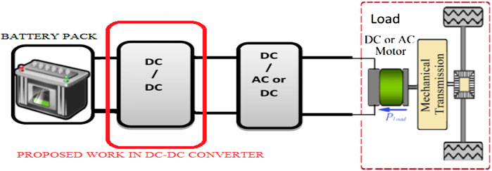
FIGURE 1. Structure of electric vehicle.
The single-phase interleaved converter in electric vehicles is incapable of supplying sufficient voltage to the transmission system (electric motor) (Chakraborty et al., 2019; Khan et al., 2021a). The proposed topology incorporates a three-phase interleaved boost converter that supplies the electric motor unit with sufficient voltage (Zaid et al., 2020; Khan et al., 2021b). The voltage gain, voltage stress, and duty cycle of the ISC converter and the conventional interleaved boost converter are compared (Khan et al., 2021c; Zaid et al., 2021). A PI controller is constructed to achieve the closed response characteristics for the proposed converter (Maalandish et al., 2017; Khan et al., 2021d). The proposed converter’s construction components are compared with the existing DC–DC converters (Li et al., 2012; Khalilzadeh and Abbaszadeh, 2015; Meier et al., 2018). Economic behavior is discussed in terms of a cost analysis of the proposed ISC converter (Aghdam and Abapour, 2016; Krishnachaitanya and Chitra, 2021). Hence, a high step-up is possible with the proposed ISC converter topology shown in Figure 2.
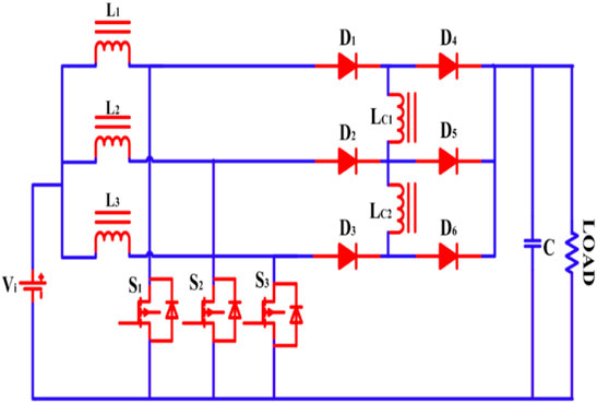
FIGURE 2. Proposed three-phase interleaved step-up DC–DC converter [ISC].
The converter topology is designed to combine a three-winding transformer between two phases, and the overall design makes a five-winding transformer. The high step-up operation produces a high output voltage to supply the motor propulsion and overcome the back emf produced in the drive. The windings L1, L2, and L3 are directly connected to the battery. The central windings LC1 and LC2 are connected to the cathodes of the diodes D1, D2, D3, and the anodes of the diodes D4, D5, and D5. Additionally, the ISC converter design consists of three power semiconductor switches (S1, S2, and S3) and an output capacitor (C) connected across the load. Additionally, a freewheeling diode is connected across the switches to freewheeling the leakage current through the switch. In this work, the three-phase interleaved boost converter is designed and validated. The steady-state analysis and state space model of this converter topology is derived. Frequency response analysis is also derived from the state space model of this converter, which proves the converter’s stability. In addition to that, the number of switches is reduced by this topology. Hence, switching losses are also being reduced in the ISC converter topology. The proposed ISC converter topology is capable of producing 139 V of output voltage and producing a power range of 881 W. Hence, this converter design attains high voltage gain and is suitable for medium and high-power applications. This proposed ISC converter design is simulated by the MATLAB/Simulink model and interfaced with the real-time simulator OPAL-RT (OP5700). The simulated outcomes clearly show that the proposed DC–DC converter is more competent and highly reliable when compared to other DC–DC converter topologies. The operational modes of the proposed ISC converter are presented in section 2. The steady-state analysis, which explains both voltage gain and voltage stress calculations, is described in section 3. In section 4, the proposed ISC converter’s state space representation is explained. For stability analysis, frequency domain calculations are conducted based on state space modeling. The experimental results and discussions are presented in section 5, economic behaviors are interpreted in terms of cost analysis in section 6 and the article is concluded in section 7.
2 Operating Modes of the Proposed ISC Converter
The structure of ISC is shown in Figure 2. The proposed ISC converter modes of operation are discussed in Figure 3. The characteristic waveforms of BCM are depicted in Figure 4A, whereas the characteristic waveforms of CCM and DCM are depicted in Figure 4B. The turn’s ratio is the ratio of the number of turns in the central winding
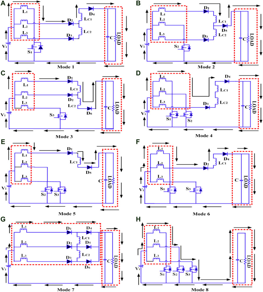
FIGURE 3. Modes of operation.
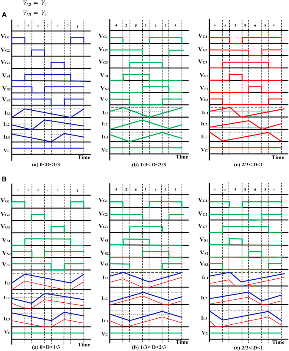
FIGURE 4. Characteristics waveforms (A) BCM (B) CCM (blue line) and DCM (red Line).
Mode 1: as shown in Figure 3A, switch S1 is initially turned on, while switches S2 and S3 are turned off. Current from the battery flows through the winding L1 and switch S1. The battery current also conducts L2 and L3. Current flows through L2 to D2, LC1, D4, C, and the load. Current flows through L3 to D3, LC2, LC1, D4, C, and the load. The voltage equation is given as
Mode 2: as Figure 3B depicts, initially the switch S2 is ON, and S1 and S3 are in an OFF condition. Current from the battery flows to the switch S2 through the winding L2. The battery current also conducts L1 and L3. Current flows through L1 to D1, LC1, D5, C, and the load. Current flows through L3 to D3, LC2, D5, C, and the load.
Mode 3: as shown in Figure 3C, the switch S3 is initially turned on, while the switches S1 and S2 are turned off. Current from the battery flows through the winding L3 and switch S3. The battery current also conducts L1 and L2. Current flows through L1 to D1, LC1, LC2, D6, C, and the load. Current flows through L2 to D2, LC2, D6, C, and the load.
Mode 4: as shown in Figure 3D, the switches S1 and S2 are initially turned on, while S3 is turned off. Current from the battery flows through the winding L1 and switch S1, and through the winding L2 and switch S2. The battery current also conducts L3, D3, LC2, LC1, D4, C, and the load. The voltage equation is given as
Mode 5: as shown in Figure 3E, the switches S2 and S3 are initially turned on, and S1 is turned off. Current from the battery flows through the winding L2 and switch S2, and through the winding L3 and switch S3. The battery current also conducts L1, D1, LC1, D5, C, and the load. The voltage equation is given as
Mode 6: as Figure 3F depicts, initially S1 and S3 are turned ON, and S2 is turned OFF. Current from the battery flows through the winding L1 and switch S1, and through the winding L3 and switch S3. The battery current also conducts L2, D2, LC1, D4, C, and the load. The voltage equation is given as
Mode 7: as Figure 3G depicts, all three switches S1, S2, and S3 are turned OFF. The battery current conducts the winding L1, L2, and L3. Battery current conducts through the windings L1 to D1, D4, C, and the load. Through L2 current conducts D2, D5, C, and the load. Through L3 current conducts D3, D6, C, and the load.
3 Steady-State Analysis
3.1 Continuous Conduction Mode (CCM)
Phase difference Ф =
The flux produced in the inductor winding is given as
The relationship between the central winding and external winding voltage is given as
Voltage gain (M) is the ratio of output voltage to the input voltage is given as
The expression for the voltage gain is given as
Figure 5 shows the relationship between voltage gain and duty cycle for the proposed ISC converter with different turns ratio. The curve clearly shows that the proposed ISC converter can provide higher output voltage than the conventional interleaved boost converter and conventional boost converter.
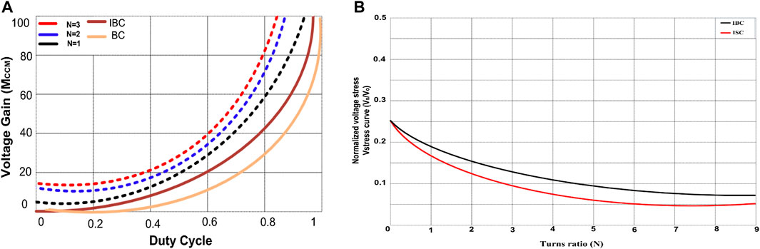
FIGURE 5. (A) Duty cycle Vs Voltage gain with different turns ratio (B) Relationship between turns ratio and switch voltage stress.
3.2 Switch Voltage Stress Calculation
The known inductor and capacitor voltages can be used to calculate all of the voltage stress on semiconductor components. The voltage stresses of the power switches and diodes are identical and they are calculated as follows:
The total voltage across the capacitor is
Since the capacitor is connected in parallel to the load, the voltage across the capacitor is equal to the output voltage.
Voltage stress of the diodes (
Figure 5A shows the Duty cycle Vs Voltage gain with different turn ratios and Figure 5B shows the relationship between voltage stress and turns ratio, N. All of the component voltage stress is lower than the output voltage Vo. The voltage stress on the power switches and diodes is less than 0.5 V. As a result, the proposed ISC converter’s semiconductor components are subjected to low voltage stress.
3.3 Input Current Ripples
The difference between the inductor’s maximum
Under identical inductor current, output voltage, and input voltage conditions, the duty cycle of the ISC converter and the conventional three-phase interleaved boost converter (IBC) may be represented as
The proposed ISC converter’s reduction in input current ripple when compared to IBC can be represented as
where
3.4 Design of the Inductor and Capacitor
The current ripple is used to design inductors, and the voltage ripple is used to design capacitors. Current ripples of the inductors and the value of inductance are given in Eqs 37, 38.
The capacitors are chosen based on the switching frequency and the output voltage ripple allowed across the capacitance-voltage connection, and other parameters are as follows:
The value of the inductor and capacitor is calculated by using Eqs 37, 39.
3.5 Discontinuous Conduction Mode (DCM)
The converter is analyzed in both continuous conduction mode and discontinuous conduction mode. In DCM, Current through the inductors can be calculated.
Mode 1: this mode is the same as CCM’s mode 1 when switch S1 is ON. The peak currents through the inductors L1, L2, and L3 can be obtained as
Mode 2: this mode is the same as CCM’s mode 2 when switch S2 is ON. The peak currents through the inductors L1, L2, and L3 can be obtained as
Mode 3: this mode is the same as CCM’s mode 3 when switch S3 is ON. The peak currents through the inductors L1, L2, and L3 can be obtained as
Mode 4: this mode is the same as CCM’s mode 4 when switch S1 and S2 are ON. The peak currents through the inductors L1, L2, and L3 can be obtained as
Mode 5: this mode is the same as CCM’s mode 5 when switch S2 and S3 are ON. The peak currents through the inductors L1, L2, and L3 can be obtained as
Mode 6: this mode is the same as CCM’s mode 6 when switch S1 and S3 are ON. The peak currents through the inductors L1, L2, and L3 can be obtained as
Mode 7: this mode is the same as CCM’s mode 7, when switch S1, S2, and S3 is OFF. The peak currents through the inductors L1, L2, and L3 can be obtained as
Mode 8: as Figure 3H depicts, all three switches S1, S2, and S3 are turned ON, inductor current of the central windings LC1 and LC2 becomes zero. Battery current flows through the windings L1 and S1, through the windings L2 and S2, and through the windings L3 and S3. Furthermore, the capacitor C is discharged into the load. The voltage equation is given as
when switch S1, S2, and S3 are ON. The peak currents through the inductors L1, L2, and L3 can be obtained as
When the volt-sec balance principle is applied to the inductors, the following relationship is obtained:
The normalized inductor time constant
With the use of Eqs 67, 69, the following quadratic function can be calculated:
Voltage gain in DCM mode is given by
3.6 Boundary Condition Mode Operation
This mode of operation allows the voltage gain of the CCM to be equivalent to the voltage gain of the DCM mode.
Figure 6 depicts the boundary normalized inductor time constant
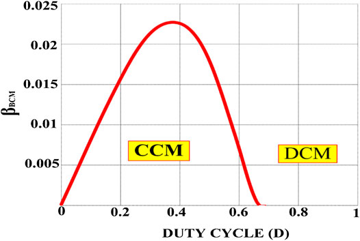
FIGURE 6. Boundary normalized inductor time constant Vs duty cycle curve.
3.7 Efficiency Calculation for the Proposed ISC Converter
The efficiency equation is computed by taking all losses into account. Input power is the sum of all the losses and the output power.
3.7.1 Power Loss in the Switches
Power loss in the switch is the sum of conduction loss and switching loss. Current through the switches S1, S2, and S3 are 2.5, 2.1, and 2.9 A, respectively and the resistance of the switches is 0.3Ω. The total power loss in the switch is 9.4 W which can be computed by the following formula:
3.7.2 Power Loss in the Capacitor
Current through the capacitor is 6.3 A and the resistance of the capacitor is 0.1Ω. The total power loss in the capacitor is 4 W which can be found by the following formula:
3.7.3 Power Loss in the Diodes
Current through the diodes is D1 to D6 is 2.5, 2.9, 3.1, 3.5, 2.8, 3.2 A and the resistance of the diodes is 0.4Ω. The total power loss in the diodes is 25.8 W which can be determined by the following formula:
3.7.4 Power Loss in the Inductor Winding
Current through the inductor is 3.2, 3.3, 3.1, 3.8, 3.6 A and the resistance of the inductor is 0.4Ω. The total power loss in the inductor is 23.2 W which can be determined by the following formula:
3.7.5 Efficiency of the Proposed ISC Converter
The output-to-input power ratio is known as efficiency. The sum of all losses and output power equals the input power. The efficiency of the proposed ISC converter is 94% which is calculated by the following formula:
4 Stability Analysis OF ISC
The state space model provides the dynamic performance of the converter circuit. It is the mathematical approach to the circuit represented in matrix form with a minimum number of equations called state variables. A state space approach is derived for both the ON and OFF states of the converter circuit. State space analysis is used to derive the transfer function of the ISC.
General state space equation of the system
Output equation
Here,
Applying KVL for mode 1 shown in Figure 3A,
State space derived for mode 1 is
Similarly, mode 2 is
Similarly, mode 3 is
Similarly, mode 4 is
Similarly, mode 5 is
Similarly, mode 6 is
Similarly, mode 7 is
Similarly, mode 8 is
where duty cycle,
The state space equation is
The output equation is
The closed loop transfer function can be derived for the proposed ISC converter topology from state space Eqs 87, 88 by MATLAB coding.
The transfer function and Bode plot are obtained by MATLAB coding from the matrices of the state space analysis. It is possible to observe the uncompensated bode plot and construct a suitable controller. Generally, a PI controller works best with lower-order systems. The uncompensated bode plot reveals that the system is stable, but contains zeros in the right half plane (Khan et al., 2021a). To maintain an appropriate phase margin, a compensator is designed to eliminate steady-state error and high-frequency disturbances. To optimize the performance of the proposed interleaved Step-up DC–DC converter [ISC], the voltage controller circuit depicted in Figure 7A evaluates both the reference and output voltages. Figure 7B shows the magnitude and phase plots of the interleaved step-up DC–DC converter [ISC]. In MATLAB, the dynamic response of an open loop and a closed loop is calculated. Although the bode plot of the uncompensated system is stable, the phase margin of the system is not desirable, which is 45°. For closed loop stability, the phase margin should be set at 79° to ensure the system has a suitable step response. Both the magnitude and phase plots of the interleaved step-up DC–DC converter are positive, indicating that the ISC circuit design will perform a stable operation. The proposed ISC converter has fewer switches, which decreases switching losses and lowers the circuit cost. The component quantity comparison is discussed in Table 1.
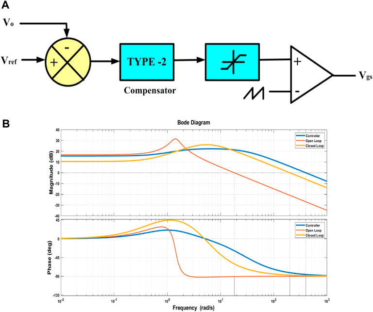
FIGURE 7. (A) voltage control loop (B) Bode plot for open loop, closed loop, and compensator.
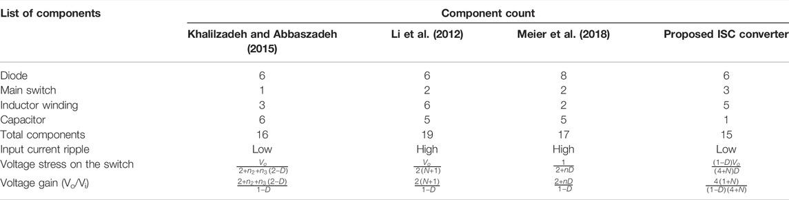
TABLE 1. Constructional components comparison of the DC–DC converters.
5 Results and Discussion
To validate the performance of the ISC converter, an 881 W real-time simulation model is built in MATLAB/Simulink and interfaced with OPAL-RT (OP5700) with the specifications defined in Table 2. The converter is operated at a duty ratio of 30 and 40% in continuous conduction mode at a switching frequency of 50 kHz with a measured input voltage of 70 V and an output voltage of 139 V. The overall real-time interfacing setup using the OP5700 is shown in Figure 8. The characteristic waveform of the switch S1, S2, and S3 are shown in Figures 9–11. The voltage across the switch S1 is 52.9V, S2 is 53.1 V and S3 is 55.2 V. Voltage across the diode D1 and the current waveforms of inductors IL1, IL2 and IL3 show that the converter is in the CCM mode of operation is shown in Figure 12. The inductor current achieves its maximum values linearly at 4.6, 3.9, and 4.2 A. Voltage across the diode D2 and current through the coil ILC1 is 3.8 A are shown in Figure 13. The converter’s input voltage and the voltage across the diode D3 Figure 14. The converter’s input current and the voltage across the diode D4 are shown in Figure 15. Capacitor voltage and the voltage across the Diode D5 are shown in Figure 16. If the duty cycle increases from 0.3 to 0.4, the output voltage rises from 65 V to 145 V. The voltage across the capacitor is as same as the output voltage. The output voltage waveform with a measured voltage of 139 V of the converter and the voltage across the diode D6 are shown in Figure 17. The current through the coil ILC2 is 3.6 A shown in Figure 18. The output current waveform with a measured current of 6.3 A for 40Ω is shown in Figure 19.
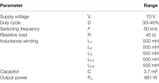
TABLE 2. Ratings of the components involved in the proposed topology.

FIGURE 8. Real-time setup using OP5700.
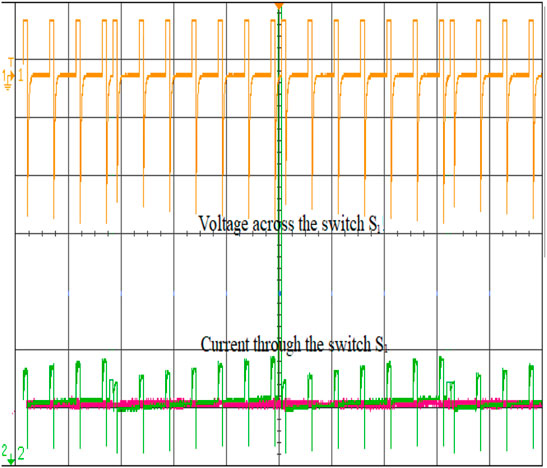
FIGURE 9. Characteristics of switch S1.
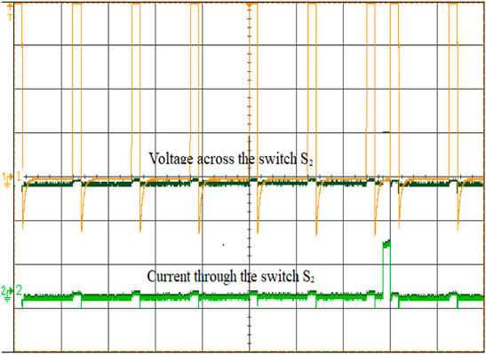
FIGURE 10. Characteristics of switch S2.

FIGURE 11. Characteristics of switch S3.
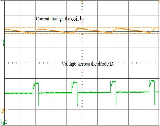
FIGURE 12. Current through the coil IL1.
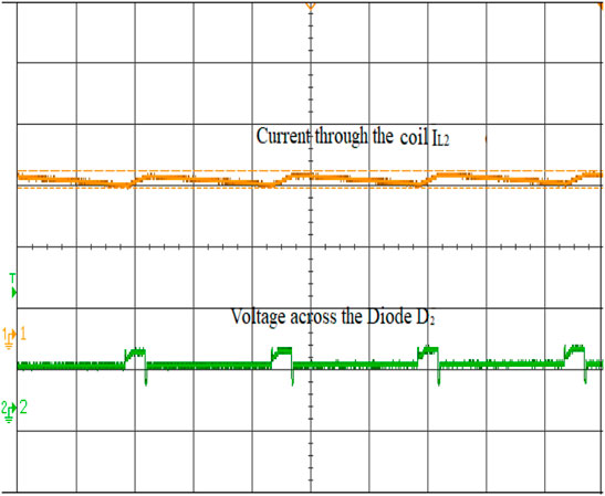
FIGURE 13. Current through the coil IL2. The voltage across the diode D1 Voltage across the diode D2.
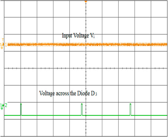
FIGURE 14. Input Voltage Vin and Diode Voltage D3.
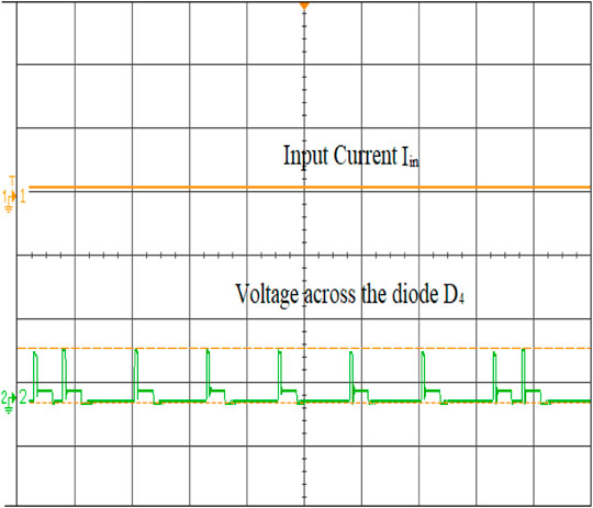
FIGURE 15. Input Current Iin and Diode Voltage D4.
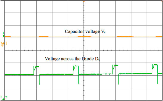
FIGURE 16. Capacitor Voltage Vc and Diode Voltage D5.
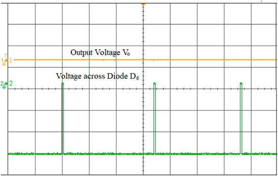
FIGURE 17. Output Voltage Vo and Diode Voltage D6.
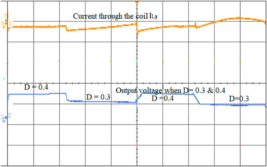
FIGURE 18. Current through ILC2 and Vout at D = 0.3 and 0.4.
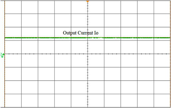
FIGURE 19. Output current of the ISC converter.
In Figure 20A, the efficiency of the converter is plotted against the output power, and when the output power increases, the efficiency gradually increases as well. The proposed converter’s efficiency increases to 94% when the output power is increased from 400 to 881 W.
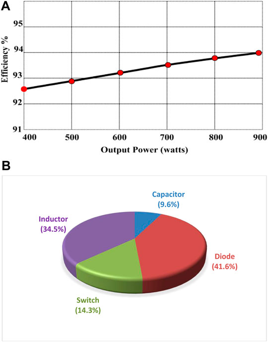
FIGURE 20. (A) ISC converter’s Efficiency with Various Output Power (B) Power Loss in various components.
The loss distribution among semiconductor components is depicted in Figure 20B. According to the same chart, the highest power loss in the diodes (D1 to D6) is 41.6%. Switch losses (S1, S2, and S3) are 14.3%. Inductors and capacitors have total losses of 34.5 and 9.6%, respectively.
6 Economic Behavior OF the ISC Converter
Once examining economic behavior, it is necessary to take switching losses and the cost function into account. The number of power switches in the topology impacts the implementation cost. The performance of the equipment is proportional to its tangible cost. Costs are categorized as variable or fixed. The cost structure varies by product. The goal of this study is to determine the converter topology’s cost. The variable cost of the product is related to the quantity manufactured, while the variable cost per unit is fixed. This results in a price discrepancy for the product; this is referred to as the “tangible cost,” and it is used to estimate the price of the equipment.
However, because the fixed cost per unit changes according to the system, selecting products based on their fixed costs may result in economic loss. This is suited for products in modest quantities. The ISC converter’s cost was estimated using a cost estimation tool that adheres to industry standards. The cost function of the ISC converter is proportional to the number of devices and DC voltage sources connected. Typically, the cost of electronics is dictated by the voltage, current, and power rating of the product. Thus, these are the components that contribute to the cost assessment of the product. Figure 21A depicts the elements included in the proposed ISC converter’s cost evaluation. The ISC Converter’s implementation costs have been divided into four categories: primary level, secondary level, tertiary level, and final level. The entire sequence necessary to determine the cost of implementing the ISC is depicted in Figure 21B. ISC converter’s total system cost comprises the initial installation cost, downtime costs, and power loss costs. The installation cost of the ISC converter comprises the investment in a power converter system. Three-phase ISC converters used in EV systems are composed of the following components: a battery, three power switches, six diodes, five inductors, and a capacitor. According to (Aghdam and Abapour, 2016), the cost of a single power MOSFET, a single inductor, a single diode, and a single capacitor is $3.6, $1.15, $1.9, and $1.5, respectively. As a result, the total cost of installation of three-phase ISC converters decreases.
Where,
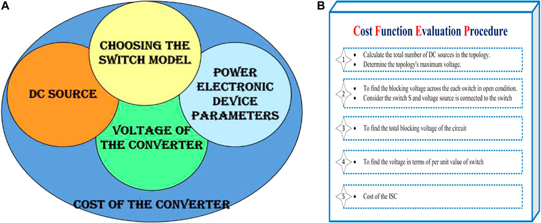
FIGURE 21. (A) Factors considered for Cost of the converter (B) Process for estimating the ISC’s implementation costs.
Downtime is defined as any period of time during which equipment is neither working nor producing. One week is necessary to replace the failed equipment. For a downtime period, a financial loss of $2.5 per hour would be assumed. To calculate downtime costs, N years and mean time between failures (MTBF) are taken into account. MTBF is the average time between system failures.
Additionally, the cost of power loss is estimated to be $0.1 per kilowatt-hour. As a result, the total cost of power loss over 1 year is as follows:
The following calculation can be used to determine the total cost of the ISC:
The total cost of the proposed converter for 15 years is $1,211.3 and for 30 years $2387.1. Cost comparison of conventional interleaved converter Vs ISC is shown in Table 3. The calculated total cost of the proposed ISC is much lower than the conventional interleaved converter. Hence, it is economical.

TABLE 3. Cost comparison of conventional interleaved converter vs. ISC.
The cost comparison clearly shows that the installation cost and the downside cost are nearly the same for both converters and that the cost of loss is higher in a conventional interleaved converter. In ISC, the cost of loss is very low than in conventional interleaved converters. Hence, the proposed ISC reduces the cost of loss. As a result, the total cost is reduced for ISC. The proposed converter excels over conventional converters in terms of switching losses, efficiency, stability, and cost function. As a result, the proposed topology can be used in commercial applications because it is economically efficient.
7 Conclusions
The three-phase interleaved step-up DC–DC converter [ISC] has been proposed, and the topology performance has been validated by the analysis of stability in the frequency domain. The proposed converter operates in both closed and open loop modes, which results in the proposed converter ensuring stable operation. The operating concepts and theoretical analysis of CCM and DCM are thoroughly explored. The proposed topology has been compared to the existing topology in terms of its constructional features, which clearly shows the proposed converter has the minimum number of switches. Due to the reduction of switches in the proposed ISC converter, which reduces switching losses and lowers the cost of making the converter circuit. Hence, it is economically efficient. The implementation of the proposed topology has been performed in the environment of MATLAB/Simulink and interfaced with OPAL-RT (OP5700). It has also been demonstrated through experimental results that voltage stress on the semiconductor components is smaller than that of the output voltage. The real-time implementation of a maximum power rating of 881 W was tested, and the maximum efficiency was observed to be 94%. Additionally, it was revealed that decreasing the input voltage reduces efficiency due to increased conduction losses. The converter performed effectively under steady-state and dynamic-state behavior, and the experimental results were consistent with the theoretical predictions. The economic behavior of ISC has been discussed and compared with the conventional interleaved converter. The overall analysis clearly shows the proposed ISC is superior in terms of voltage gain, switching losses, efficiency, stability, and cost function. Since this topology is promising for EV applications.
8 Future Scope
At a future point, a bidirectional version of the proposed ISC converter topology could be developed, with both step-up and step-down operations performed in the same circuit. At present, the converter is in step-up mode. The switches are connected in parallel with the diode. Once the main switch is turned off, the device enters step-down mode, and energy is saved in the battery, thereby achieving bidirectional operation. Bidirectional mode refers to the flow of power from the source to the load and vice versa. Furthermore, soft switching techniques are used. To minimize switching losses, soft switching approaches employ resonant mechanisms to turn on at zero voltage and turn off at zero current. The reliability, stability, switching losses, economic efficiency, and economic behavior of the bidirectional version of the proposed ISC converter topology will be incorporated.
Data Availability Statement
The original contributions presented in the study are included in the article/Supplementary Materials; further inquiries can be directed to the corresponding author.
Author Contributions
All authors listed have made a substantial, direct, and intellectual contribution to the work and approved it for publication.
Conflict of Interest
The authors declare that the research was conducted in the absence of any commercial or financial relationships that could be construed as a potential conflict of interest.
Publisher’s Note
All claims expressed in this article are solely those of the authors and do not necessarily represent those of their affiliated organizations, or those of the publisher, the editors, and the reviewers. Any product that may be evaluated in this article, or claim that may be made by its manufacturer, is not guaranteed or endorsed by the publisher.
Supplementary Material
The Supplementary Material for this article can be found online at: https://www.frontiersin.org/articles/10.3389/fenrg.2022.813081/full#supplementary-material
References
Aghdam, F. H., and Abapour, M. (2016). Reliability and Cost Analysis of Multistage Boost Converters Connected to PV Panels. IEEE J. Photovoltaics 6 (4), 981–989. doi:10.1109/JPHOTOV.2016.2566885
Athikkal, S., Guru Kumar, G., Sundaramoorthy, K., and Sankar, A. (2018). Performance Analysis of a Positive Output Voltage Dual Input Dc–Dc Converter for Hybrid Energy Application. J.Circ., Syst. Comput. 27 (1–22), 1850159. doi:10.1142/S0218126618501591
Babaei, E., Mashinchi Maheri, H., Sabahi, M., and Hosseini, S. H. (2018). Extendable Nonisolated High Gain DC-DC Converter Based on Active-Passive Inductor Cells. IEEE Trans. Ind. Electron. 65, 9478–9487. doi:10.1109/TIE.2018.2807367
Babaei, E., Saadatizadeh, Z., and Ivatloo, B. M. (2017). A New Interleaved Bidirectional Zero Voltage Switching DC/DC Converter with High Conversion Ratio. J.Circ., Syst. Comput. 26 (1–25), 1750105. doi:10.1142/S0218126617501055
Bharathidasan, M., Indragandhi, V., Kuppusamy, R., Teekaraman, Y., Urooj, S., and Alwad, N. (2022). Intelligent Fuzzy Based High Gain Non-isolated Converter for DC Micro-grids. Comput. Mater. Continua 71 (2), 4069–4084. doi:10.32604/cmc.2022.021846
Bonab, H. A. F., Banaei, M. R., and Kalantari, N. T. (2018). A Voltage Multiplier Based High Voltage Gain Transformerless Buck–Boost DC–DC Converter. J.Circ., Syst. Comput. 27 (1–21), 1850188. doi:10.1142/S0218126618501888
Chakraborty, S., Vu, H.-N., Hasan, M. M., Tran, D.-D., El Baghdadi, M. E., and Hegazy, O. (20192019). DC-DC Converter Topologies for Electric Vehicles, Plug-In Hybrid Electric Vehicles and Fast Charging Stations: State of the Art and Future Trends. Energies 12, 1569. doi:10.3390/en12081569
Guilbert, D., Gaillard, A., N'Diaye, A., and Djerdir, A. (2016). Power Switch Failures Tolerance and Remedial Strategies of a 4-leg Floating Interleaved DC/DC Boost Converter for Photovoltaic/fuel Cell Applications. Renew. Energy 90, 14–27. doi:10.1016/j.renene.2015.12.054
Guilbert, D., Guarisco, M., Gaillard, A., N'Diaye, A., and Djerdir, A. (2015). FPGA Based Fault-Tolerant Control on an Interleaved DC/DC Boost Converter for Fuel Cell Electric Vehicle Applications. Int. J. Hydrogen Energy 40, 15815–15822. doi:10.1016/j.ijhydene.2015.03.124
Gupta, N., Bhaskar, M. S., Almakhles, D., Sanjeevikumar, P., Subramaniam, U., Leonowicz, Z., et al. (20202020). “Novel Non-isolated Quad-Switched Inductor DoubleSwitch Converter for DC Microgrid Application,” in IEEE International Conference on Environment and Electrical Engineering and 2020 IEEE Industrial and Commercial Power Systems Europe (EEEIC/I&CPS Europe) (Madrid, Spain: IEEE), 1–6. doi:10.1109/EEEIC/ICPSEurope49358.2020.9160839
Hasan, N. S., Rosmin, N., Osman, D. A. A., and Musta’amal, A. H. (2017). Reviews on Multilevel Converter and Modulation Techniques. Renew. Sustain.Energy Rev. 80, 163–174. doi:10.1016/j.rser.2017.05.163
Hegazy, O., Van Mierlo, J., and Lataire, P. (2012). Analysis, Modeling, and Implementation of a Multidevice Interleaved DC/DC Converter for Fuel Cell Hybrid Electric Vehicles. IEEE Trans. Power Electron 27, 4445–4458. doi:10.1109/tpel.2012.2183148
Kabalo, M., Paire, D., Blunier, B., Bouquain, D., Simões, M. G., and Miraoui, A. (2013). Experimental Evaluation of Four- Phase Floating Interleaved Boost Converter Design and Control for Fuel Cell Applications. IET Power Electron 6, 215–226. doi:10.1049/iet-pel.2012.0221
Kabalo, M., Paire, D., Blunier, B., Bouquain, D., Simões, M. G., and Miraoui, A. (2012). Experimental Validation of High- Voltage-Ratio Low-Input-Current-Ripple Converters for Hybrid Fuel Cell Supercapacitor Systems. IEEE Trans. Veh. Technol. 61, 3430–3440. doi:10.1109/tvt.2012.2208132
Karthikeyan, V., Kumaravel, S., and Gurukumar, G. (2019). High Step-Up Gain DC-DC Converter with Switched Capacitor and Regenerative Boost Configuration for Solar PV Applications. IEEE Trans. Circuits Syst. II Express Briefs 66, 122022–122026. doi:10.1109/TCSII.2019.2892144
Khalilzadeh, M., and Abbaszadeh, K. (2015). Non-isolated High Step-Up DC–DC Converter Based on Coupled Inductor with Reduced Voltage Stress. IET Power Electron. 8, 2184–2194. doi:10.1049/iet-pel.2014.0899
Khan, S., Mahmood, A., Tariq, M., Zaid, M., Khan, I., and Rahman, S. (2021c). “Improved Dual Switch Non-isolated High Gain Boost Converter for DC Microgrid Application,” in 2021 IEEE Texas Power and Energy Conference (TPEC) (IEEE), 1–6. doi:10.1109/TPEC51183.2021.9384956
Khan, S., Mahmood, A., Zaid, M., Tariq, M., Lin, C.-H., Ahmad, J., et al. (2021a). A High Step-Up DC-DC Converter Based on the Voltage Lift Technique for Renewable Energy Applications. Sustainability 13 (19), 11059. doi:10.3390/su131911059
Khan, S., Mahmood, A., Zaid, M., Tariq, M., and Sadaf, S. (2020). “A Single Inductor, Single Switch High Gain DC-DC Boost Converter,” in IEEE International Women in Engineering (WIE) Conference on Electrical and Computer Engineering (WIECON-ECE) (IEEE), 98–101. doi:10.1109/WIECON-ECE52138.2020.9398038
Khan, S., Varshney, K., Zaid, M., Tariq, M., Ahmad, J., and Sarwer, Z. (2021d). “A Single Input Dual Output High Gain DC-DC Converter with Reduced Voltage Stress,” in IECON 2021 – 47th Annual Conference of the IEEE Industrial Electronics Society (IEEE), 1–6. doi:10.1109/IECON48115.2021.9589488
Khan, S., Zaid, M., Mahmood, A., Nooruddin, A. S., Ahmad, J., Alghaythi, M. L., et al. (2021b). A New Transformerless Ultra High Gain DC–DC Converter for DC Microgrid Application. IEEE Access 9, 124560–124582. doi:10.1109/ACCESS.2021.3110668
Kirubakaran, A., Jain, S., and Nema, R. K. (2009). A Review on Fuel Cell Technologies and Power Electronic Interface. Renew. Sustain. Energy Rev. 13, 2430–2440. doi:10.1016/j.rser.2009.04.004
Kolli, A., Gaillard, A., De Bernardinis, A., Bethoux, O., Hissel, D., and Khatir, Z. (2015). A Review on DC/DC Converter Architectures for Power Fuel Cell Applications. Energy Convers. Manag. 105, 716–730. doi:10.1016/j.enconman.2015.07.060
Krishnachaitanya, D., and Chitra, A. (2021). Quantitative Analysis of Asymmetric Multilevel Inverters with Reduced Device Count from Reliability and Cost Function Perspective—A Review. IEEE Trans. Power Electron. 36 (10), 11068–11086. doi:10.1109/TPEL.2021.3071375
Lee, P.-W., Lee, Y.-S., Cheng, D. K. W., and Liu, X.-C. (2000). Steady-state Analysis of an Interleaved Boost Converter with Coupled Inductors. IEEE Trans. Industrial Electron. 47 (4), 787–795. doi:10.1109/41.857959
Li, W., Zhao, Y., Wu, J., and He, X. (2012). Interleaved High Step-Up Converter with Winding-Cross-Coupled Inductors and Voltage Multiplier Cells. IEEE Trans. Power Electron. 27 (1), 133–143. doi:10.1109/TPEL.2009.2028688
Maalandish, M., Hosseini, S. H., Ghasemzadeh, S., Babaei, E., Shalchi Alishah, R., and Jalilzadeh, T. (2017). Six-phase Interleaved Boost Dc/dc Converter with High-Voltage Gain and Reduced Voltage Stress. IET Power Electron. 10 (14), 1904–1914. doi:10.1049/ietpel.2016.1029
Meier, M. B., Avelino da Silva, S., Badin, A. A., Romaneli, E. F. R., and Gules, R. (2018). Soft-Switching High Static Gain DC–DC Converter without Auxiliary Switches. IEEE Trans. Industrial Electron. 65 (3), 2335–2345. doi:10.1109/TIE.2017.2739684
Padala, S. R., and Yeddula, P. (2022). A Non‐isolated Switched Inductor‐capacitor Cell Based Multiple High Voltage Gain DC‐DC Boost Converter. Int. J. Circuit Theory Appl, 1–25. doi:10.1002/cta.3239
Reddy, K. J., and Sudhakar, N. (2018). High Voltage Gain Interleaved Boost Converter with Neural Network Based MPPT Controller for Fuel Cell Based Electric Vehicle Applications. IEEE Access 6, 3899–3908. doi:10.1109/access.2017.2785832
Saadi, R., Hammoudi, M. Y., Kraa, O., Ayad, M. Y., and Bahri, M. (2020). A Robust Control of a 4-leg Floating Interleaved Boost Converter for Fuel Cell Electric Vehicle Application. Math. Comput. Simul. 167, 32–47. doi:10.1016/j.matcom.2019.09.014
Saravanan, S., Karunanithi, K., and Pragaspathy, S. (2020). A Novel Topology for Bidirectional Converter with High Buck Boost Gain. J. Circ. Syst. Comput. 27, 2050222. doi:10.1142/s0218126620502229
Wang, Y.-X., Yu, D.-H., Chen, S.-A., and Kim, Y.-B. (2014a). Robust DC/DC Converter Control for Polymer Electrolyte Membrane Fuel Cell Application. J. Power Sources 261, 292–305. doi:10.1016/j.jpowsour.2014.03.048
Wang, Y.-X., Yu, D.-H., and Kim, Y.-B. (2014b). Robust Time-Delay Control for the DC–DC Boost Converter. IEEE Trans. Ind. Electron. 61, 4829–4837. doi:10.1109/tie.2013.2290764
Wen, H., and Su, B. (2015). Practical Implementation of an Interleaved Boost Converter for Electric Vehicle Applications. J. Power Electron 15, 1035–1046. doi:10.6113/jpe.2015.15.4.1035
Yao, T., Nan, C., and Ayyanar, R. (2018). A New Soft-Switching Topology for Switched Inductor High Gain Boost. IEEE Trans. Industry Appl. 54 (3), 2449–2458. doi:10.1109/tia.2018.2791972
Zaid, M., Lin, C-H., Khan, S., Ahmad, J., Tariq, M., Mahmood, A., et al. (2021). A Family of Transformerless Quadratic Boost High Gain DC-DC Converters. Energies 14 (14), 4372. doi:10.3390/en14144372
Zaid, M., Ahmad, J., Sarwar, A., Sarwer, Z., Tariq, M., and Alam, A. (2020). “A Transformerless Quadratic Boost High Gain DC-DC Converter,” in 2020 IEEE International Conference on Power Electronics, Drives and Energy Systems (PEDES) (IEEE), 1–6. doi:10.1109/PEDES49360.2020.9379778
Zhang, G., Jin, N., Qu, L., and Yu, S. S. (2020). Inherently Non-pulsating Input Current DC-DC Converter for Battery Storage Systems. IEEE Access 8, 140293–140302. doi:10.1109/ACCESS.2020.3012709
Zhuo, S., Arnaud, G., Guo, L., Xu, L., Paire, D., and Gao, F. (2019a). Active Disturbance Rejection Voltage Control of Floating Interleaved DC-DC Boost Converter with Switch Fault Consideration. IEEE Trans. Power Electron. 34 (12), 12396–12406. doi:10.1109/tpel.2019.2905897
Keywords: step-up converter, interleaved converter, state space model, Bode plot, electric vehicles
Citation: Saravanakumar T and Saravana kumar R (2022) Design, Validation, and Economic Behavior of a Three-Phase Interleaved Step-Up DC–DC Converter for Electric Vehicle Application. Front. Energy Res. 10:813081. doi: 10.3389/fenrg.2022.813081
Received: 11 November 2021; Accepted: 28 April 2022;
Published: 02 June 2022.
Edited by:
Antonio J. Marques Cardoso, University of Beira Interior, PortugalReviewed by:
Mohd Tariq, Aligarh Muslim University, IndiaAravind C K, Mepco Schlenk Engineering College, India
Fernando Bento, University of Beira Interior, Portugal
Copyright © 2022 Saravanakumar and Saravana kumar. This is an open-access article distributed under the terms of the Creative Commons Attribution License (CC BY). The use, distribution or reproduction in other forums is permitted, provided the original author(s) and the copyright owner(s) are credited and that the original publication in this journal is cited, in accordance with accepted academic practice. No use, distribution or reproduction is permitted which does not comply with these terms.
*Correspondence: R. Saravana kumar, cnNhcmF2YW5ha3VtYXJAdml0LmFjLmlu