 Hassan Yousif Ahmed1*
 Omar Abdel-Rahim
 Ziad M. Ali
- 1College of Engineering at Wadi Addawaser, Prince Sattam Bin Abdulaziz University, Al-Kharj, Saudi Arabia
- 2Electrical Engineering Department, Faculty of Engineering, Aswan University, Aswan, Egypt
Due to the low voltage of the PV module and to enable AC module technology, where every PV module has its own DC-AC converter, this paper introduces a new high step-up seven-level two-stage multilevel inverter for a grid-connected Photovoltaic (PV) system. The introduced schematic consists of two stages. The first stage is a switched capacitor boost converter and the second stage is a seven-level seven-switches multilevel inverter. The first stage is designed to extract the maximum power of PV module and step-up its input voltage. The proposed seven-level seven-switches topology generates seven levels with only seven switches. Thus, the number of switches is reduced. The proposed inverter has eight valid switching states. In each switching state only three switches are ON at the same time. The proposed topology has some distinct features such as reduced number of switches and reduced conduction; total harmonic distortion (THD) of the current is 23% in case of pure resistive and with no filtration at the output and less than 3% using a small filter with integration into the grid. Due to the high boosting ability of the switched capacitor boost converter, a wide voltage gain is easily achievable. In this paper the system is tested at different voltage gains and the highest simulated efficiency was around 96%. The developed system is simulated in MATLAB/SIMULINK and in real time using DSPACE1202. Both simulation and real-time results are consistent with the theoretical analysis.
Introduction
Renewable energy is now essential in order to reduce pollution and to keep climate change under control. Photovoltaic (PV) power generation is one of the leading forms of renewable power generation, especially in residential power generation. PV module-generated voltage is small and requires a step-up converter to match with load requirement and extract the maximum power from the module. A DC-AC conversion stage is mandatory in case of AC grid integration. Different inversion topologies have been reported in the literature, however multilevel inverters are gaining more attention due to their inherent merits as their output voltage is in a staircase shape, which reduces filter requirements and enables the utilization of low rating switching devices (Jeevananthan et al., 2006; Mondal et al., 2009; Rahim et al., 2011).
Multilevel inverters are classified based on their structure into three main categories: Cascaded H-Bridge (CHB)topologies, Flying Capacitor (FC), and Neutral Point Clamped (NPC) (Rajeevan et al., 2011).
NPC inverters are widely used configurations in the industry and are well identified by academia, where DC-link voltage is split by means of a series of connected capacitors (Saeedifard et al., 2012; Tian et al., 2018). However, special consideration should be made to keep the balance of the split capacitors (Sebaaly et al., 2016; Akagi, 2017; Giri et al., 2017; Hu et al., 2017). FC is another style of multilevel topologies where floating capacitors are used to generate the required voltage levels. Similar to NPC, special care should be given to floating capacitors voltage balance as they are utilizing a large number of capacitors for higher voltage levels (Amini et al., 2016; Amini and Moallem, 2017; Lei et al., 2017). CHB multilevel configuration is implemented by a series of connections of H-bridges. Each H-bridge is connected to an isolated DC-voltage source. The number of bridges connected in a series are based on the required voltage level (Wu et al., 2017; Iqbal et al., 2020). Owing to the modularity of this structure and straightforwardness of its control, it is very convenient to use in high-power applications (Pulikanti et al., 2013; Wang et al., 2017; Siddique et al., 2021). One disadvantage of such a structure is the number of isolated DC-DC sources increases with any increasing number of voltage levels (Babaei and Hosseini, 2009; Malinowski et al., 2010; Gautam et al., 2017).
Switched Capacitor Multilevel Inverter (SCMLI) is a good candidate for PV applications, due to its boosting ability. In SCMLI, capacitors are charged from the PV module and discharge their energy into the load in different series and parallel combinations to achieve higher voltage at the output (Roy et al., 2021). SCMLI presented in Taghvaie et al. (2018) works on reducing the maximum voltage stress of switches by eliminating the h-bridge part. However, it utilized a bigger number of switches to achieve the required voltage level. Authors in Khoun Jahan et al. (2019) modified the CHB inverter by replacing the DC sources with switched capacitors. However, switches are controlled to sustain the balance of the switched capacitors. The seven-level SCMLI proposed in Siddique et al. (2020a) utilizes only two switched capacitors to realize the seven levels but with a large number of switching devices.
A general schematic of the proposed system is shown in Supplementary Figure S1. PV panel is connected to switched capacitor boost (SC-boost) converter. SC-boost converter extracts the maximum power from the PV panel and generates a three-level output voltage: Vco1, Vco2, and Vco3. The voltage on the three switched capacitor is utilized by the novel seven-level multilevel inverter to provide high-quality output voltage or to be integrated with the grid voltage. A control system is also divided into two parts: The maximum Power Point Tracking (MPPT) control part, which is used to control the SC-boost DC/DC converter to extract the maximum power from the PV panel, and the PI control with level-shift PWM to control the switches of the proposed seven-level multilevel inverter to control the output voltage in case of islanded operation or control the output current in case of grid integration case.
Proposed Switched Capacitor Seven Level Multilevel Inverter
The structure of the proposed two-stage switched-capacitor boost multilevel inverter is shown in Supplementary Figure S2. SC-Boost converter developed in (Tran et al., 2018; Farhadi-Kangarlu and Marangalu, 2019) is used as the first stage to boost PV voltage to a higher voltage level and extract maximum power from the PV panel; its three output switched capacitor is used as input to the proposed seven-level multilevel inverter. The proposed multilevel inverter is shown in Supplementary Figure S3.
It consists of seven switches, one of them, switch S3, is without an antibody diode. Two switches are operating at a fundamental frequency, S5 and S7, and are operating in a complementary manner. In each switching state, only three switches are conducting at the same time. Output voltage is a staircase of seven levels. The inverter has eight valid switching states, as shown in Supplementary Figure S4 and Table 1.
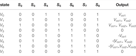
TABLE 1. Switching states of the seven-level multilevel inverter.
Mode 1 takes place by activating switches S4, S5, and S8 and deactivating switches S2, S3, S6, and S7. Output voltage is equal to capacitor Co1 voltage Vco1 (see Supplementary Figure S4A).
Mode 2 In order to achieve this mode, switches S3, S5, and S8 are ON, while switches S2, S4, S6, and S7 are OFF. Output voltage is equal to the sum of capacitor Co1 voltage and capacitor Co2 voltage, Vco1+Vco2 (see Supplementary Figure S4B.
Mode 3 occurs by activating switches S2, S5, and S8 and deactivating switches S3, S4, S6, and S7. Output voltage is equal to the sum of capacitor Co1 voltage, capacitor Co2 voltage, and capacitor Co3 voltage, Vco1 + Vco2+Vco3 (see Supplementary Figure S4C)
Mode 4 represents a freewheeling mode, where the output voltage is zero. As illustrated in Supplementary Figure S4D, switches S5 and S6 are ON, while switches S2, S3, S4, S6, and S7 are OFF.
Mode 5 takes place by activating switches S4, S6, and S7, and deactivating switches S2, S3, S5, and S8. Output voltage is equal to the negative of capacitor Co1 voltage Vco1 (see Supplementary Figure S4E).
Mode 6 occurs by triggering switches S3, S6, and S7 ON and triggering switches S2, S4, S5, and S8 OFF. Output voltage is equal to the negative of the sum of capacitor Co1 voltage and capacitor Co2 voltage, switches, while switches, -(Vco2+Vco1) (see Supplementary Figure S4F) of capacitor Co1 voltage, capacitor Co2 voltage, and capacitor Co3 voltage., -(Vco2+ Vco3+Vco1) (see Supplementary Figure S4G).
Mode 8 is a freewheeling mode; output voltage is zero. Switches S7 and S8 are ON, while switches S2, S3, S4, S6, and S5 are OFF (see Supplementary Figure S4H).
Table 2 is a comparison between previously published 7-level inverters and the proposed one. The proposed converter has an optimum number of components plus the ability to step-up voltage.
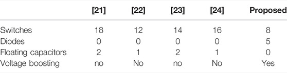
TABLE 2. Comparison between different 7-level multilevel converters.
The voltage gain of the converter is obtained considering the steady state analysis of the DC-DC converter, as below:
Charge state, which is illustrated in Supplementary Figure S5A, occurs when switch S1 is turned on, activating the main switch capacitors C1, and C2 to be connected in parallel with output capacitors Co1 and Co2, and the main characteristic equation of this mode is as follow,
Discharge state, which is illustrated in Supplementary Figure S5B, occurs when main switch S1 is turned off. Inductors and supply are charging the output capacitors; main characteristic equation of this mode as follow:
Considering the two modes, the voltage gain of the converter is given as:
A graph of the converter voltage gain is illustrated in Supplementary Figure S6, where the converter step-up ability is 3 times that of a traditional boost converter. Voltage and current stress of circuit-switching devices are illustrated in Table 3.
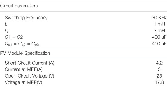
TABLE 3. Circuit parameters.
Control Approach
A block diagram of the control system is depicted in Supplementary Figure S7A. As illustrated in the figure, PV voltage and current are measured and an MPPT control technique is applied to extract the maximum power from the PV. MPPT algorithm generates a reference signal to the PI controller. The reference signal generated by the MPPT is multiplied by unity amplitude sinusoidal waveform. PI controller is used to control the output voltage of the multilevel inverter in case of islanded operation or control the output current in case of a grid-connected system.
Level-Shift Pulse Width Modulation (LS-PWM) is generated to control the 7-level inverter proposed in this paper (Baksi and Behera, 2021), see Supplementary Figure S7B. Switching pattern of different switching devices is depicted in Supplementary Figure S8.
Results and Discussions
In order to validate the proper operation of the proposed system, the system is simulated using MATLAB/SIMULINK platform; system parameters are given in Table 3. PV panel is controlled to generate its maximum power under different operating conditions. P&O algorithm is applied to the DC-DC converter to extract the maximum power from the PV panel. The algorithm introduces a perturbation
Once the algorithm reaches near the MPP, the process will go backward and forward around the MPP (see Supplementary Figure S9). PV panel is operating at its maximum power under different environmental conditions (see Supplementary Figure S9), an abrupt change in solar radiation takes place, and the controller extracts the maximum power in an efficient way. In Supplementary Figure S10A, the system is investigated under a resistive load. Output voltage is a staircase with seven levels, same as the load current. Capacitors Co1, Co2, and Co3 voltages are also displayed in the same graph. Supplementary Figure S10B is another case study with inductive load, output voltage, current, and capacitors voltage depicted in the graph. The grid integration case of the study is also considered; the proposed system is connected to the grid and its output is depicted in Supplementary Figure S11.
In order to investigate the system performance and assure its proper operation, the system is experimentally demonstrated using DSPACE 1202. Different cases of studies are investigated and the results are depicted in Supplementary Figure S12. Supplementary Figure S12A represents the output where the load is resistive and Supplementary Figure S12B represent an inductive load case. The obtained results are consistent with simulation results. In order to test system efficiency under different step up-points, the system is simulated at different power levels and different step-up ratios. Simulated efficiency results are illustrated in Supplementary Figure S17.
Conclusion
Two-stage boost multilevel inverter is presented in this paper. The first stage is based on SC-Boost converter to boost PV low voltage and extract maximum power from the PV panel, and its switched capacitor serves as input sources to the second stage. The second stage of the two-stage inverter is constructed from a novel seven-level multilevel inverter to generate seven-level output voltage. The proposed seven level inverter has some distinct features such as its compact size, low cost, reduced number of switches, and less condition loss. This is because it is constructed from only seven switches and has eight possible switching states. In each switching state, three switches are ON at the same time. Level shift PWM is implemented to drive the switches of the multilevel inverter. Different case studies have been considered in simulation and in real-time simulation, with resistive load, inductive load, and a grid-connection case (Tian et al., 2018; Saeedifard et al., 2012; Wang et al., 2017; Pulikanti et al., 2013; Siddique et al., 2021; Siddique et al., 2020b; Iqbal et al., 2020; Wu et al., 2017).
Data Availability Statement
The original contributions presented in the study are included in the article/Supplementary Material, further inquiries can be directed to the corresponding authors.
Author Contributions
OA-R designed and performed the simulations and obtained the results; OA-R, HY, and ZM analyzed the obtained results. OA-R and ZM wrote the paper, which was further reviewed by HY. All authors have read and agreed to the published version of the manuscript.
Conflict of Interest
The authors declare that the research was conducted in the absence of any commercial or financial relationships that could be construed as a potential conflict of interest.
Publisher’s Note
All claims expressed in this article are solely those of the authors and do not necessarily represent those of their affiliated organizations, or those of the publisher, the editors and the reviewers. Any product that may be evaluated in this article, or claim that may be made by its manufacturer, is not guaranteed or endorsed by the publisher.
Acknowledgments
The authors extend their appreciation to the Deputyship for the Research & innovation, Ministry of Education in Saudi Arabia for funding this research work through the project number (IF-PSAU-2021/01/18678).
Supplementary Material
The Supplementary Material for this article can be found online at: https://www.frontiersin.org/articles/10.3389/fenrg.2022.869662/full#supplementary-material
References
Akagi, H. (2017). Multilevel Converters: Fundamental Circuits and Systems. Proc. IEEE 105 (11), 2048–2065. doi:10.1109/jproc.2017.2682105
Amini, J., and Moallem, M. (2017). A Fault-Diagnosis and Fault-Tolerant Control Scheme for Flying Capacitor Multilevel Inverters. IEEE Trans. Ind. Electron. 64 (3), 1818–1826. doi:10.1109/tie.2016.2624722
Amini, J., Viki, A. H., Radan, A., and Moallem, M. (2016). A General Active Capacitor Voltage Regulating Method for L-Level M-Cell N-phase Flying Capacitor Multilevel Inverter with Arbitrary DC Voltage Distribution. IEEE Trans. Ind. Electron. 63 (5), 2659–2668. doi:10.1109/tie.2016.2517058
Babaei, E., and Hosseini, S. H. (2009). New Cascaded Multilevel Inverter Topology with Minimum Number of Switches. Energ. Convers. Manag. 50 (11), 2761–2767. doi:10.1016/j.enconman.2009.06.032
Baksi, S. K., and Behera, R. K. (2021). “A Reduced Switch Count 7-Level Boost ANPC Inverter Topology for Photovoltaic Application,” in Proceeding of the 2021 IEEE 2nd International Conference on Smart Technologies for Power, Energy and Control (STPEC), Bilaspur, Chhattisgarh, India, Dec. 2021 (IEEE), 1–6. doi:10.1109/STPEC52385.2021.9718671
Farhadi-Kangarlu, M., and Marangalu, M. G. (2019). “A Single DC-Source Five-Level Inverter Applied in Stand-Alone Photovoltaic Systems Considering MPPT Capability,” in Proceeding of the 2019 10th International Power Electronics, Drive Systems and Technologies Conference (PEDSTC), Shiraz, Iran, Feb. 2019 (IEEE), 338–342. doi:10.1109/pedstc.2019.8697896
Gautam, S. P., Gupta, S., and Kumar, L. (2017). Reliability Improvement of Transistor Clamped H‐bridge‐based Cascaded Multilevel Inverter. IET Power Elect. 10 (7), 770–781. doi:10.1049/iet-pel.2016.0574
Giri, S. K., Chakrabarti, S., Banerjee, S., and Chakraborty, C. (2017). A Carrier-Based PWM Scheme for Neutral Point Voltage Balancing in Three-Level Inverter Extending to Full Power Factor Range. IEEE Trans. Ind. Electron. 64 (3), 1873–1883. doi:10.1109/tie.2016.2624721
Hu, C., Yu, X., Holmes, D. G., Shen, W., Wang, Q., Luo, F., et al. (2017). An Improved Virtual Space Vector Modulation Scheme for Three-Level Active Neutral-Point-Clamped Inverter. IEEE Trans. Power Electron. 32 (10), 7419–7434. doi:10.1109/tpel.2016.2621776
Iqbal, A., Siddique, M. D., Ali, J. S. M., Mekhilef, S., and Lam, J. (2020). A New Eight Switch Seven Level Boost Active Neutral Point Clamped (8S-7l-BANPC) Inverter. IEEE Access 8, 203972–203981. doi:10.1109/ACCESS.2020.3036483
Jeevananthan, S., Madhavan, R., Padmanabhan, T. S., and Dananjayan, P. (2006). “State-of-the-art of Multi-Carrier Modulation Techniques for Seven Level Inverter: A Critical Evaluation and Novel Submissions Based on Control Degree of freedom,” in Proceeding of the IEEE International Conference on Industrial Technology, Mumbai, India, Dec. 2006 (IEEE), 1269–1274. doi:10.1109/icit.2006.372400
Khoun Jahan, H., Abapour, M., and Zare, K. (2019). Switched-capacitor-based Single-Source Cascaded H-Bridge Multilevel Inverter Featuring Boosting Ability. IEEE Trans. Power Electron. 34 (2), 1113–1124. doi:10.1109/tpel.2018.2830401
Lei, Y., Barth, C., Qin, S., Liu, W.-C., Moon, I., Stillwell, A., et al. (2017). A 2-kW Single-phase Seven-Level Flying Capacitor Multilevel Inverter with an Active Energy Buffer. IEEE Trans. Power Electron. 32 (11), 8570–8581. doi:10.1109/tpel.2017.2650140
Malinowski, M., Gopakumar, K., Rodriguez, J., and Pérez, M. A. (2010). A Survey on Cascaded Multilevel Inverters. IEEE Trans. Ind. Electron. 57 (7), 2197–2206. doi:10.1109/tie.2009.2030767
Mondal, G., Sivakumar, K., Ramchand, R., Gopakumar, K., and Levi, E. (2009). A Dual Seven-Level Inverter Supply for an Open-End Winding Induction Motor Drive. IEEE Trans. Ind. Electron. 56 (5), 1665–1673. doi:10.1109/tie.2008.2010159
Pulikanti, S. R., Konstantinou, G., and Agelidis, V. G. (2013). Hybrid Seven-Level Cascaded Active neutral-point-clamped-based Multilevel Converter under SHE-PWM. IEEE Trans. Ind. Electron. 60 (11), 4794–4804. doi:10.1109/tie.2012.2218551
Rahim, N. A., Chaniago, K., and Selvaraj, J. (2011). Single-phase Seven-Level Grid-Connected Inverter for Photovoltaic System. IEEE Trans. Ind. Electron. 58 (6), 2435–2443. doi:10.1109/tie.2010.2064278
Rajeevan, P. P., Sivakumar, K., Patel, C., Ramchand, R., and Gopakumar, K. (2011). A Seven-Level Inverter Topology for Induction Motor Drive Using Two-Level Inverters and Floating Capacitor Fed H-Bridges. IEEE Trans. Power Electron. 26 (6), 1733–1740. doi:10.1109/tpel.2010.2090541
Roy, T., Tesfay, M. W., Nayak, B., and Panigrahi, C. K. (2021). A 7-Level Switched Capacitor Multilevel Inverter with Reduced Switches and Voltage Stresses. IEEE Trans. Circuits Syst. 68 (12), 3587–3591. doi:10.1109/TCSII.2021.3078903
Saeedifard, M., Barbosa, P. M., and Steimer, P. K. (2012). Operation and Control of a Hybrid Seven-Level Converter. IEEE Trans. Power Electron. 27 (2), 652–660. doi:10.1109/tpel.2011.2158114
Sebaaly, F., Vahedi, H., Kanaan, H. Y., Moubayed, N., and Al-Haddad, K. (2016). Design and Implementation of Space Vector Modulation-Based Sliding Mode Control for Grid-Connected 3L-NPC Inverter. IEEE Trans. Ind. Electron. 63 (12), 7854–7863. doi:10.1109/tie.2016.2563381
Siddique, M. D., Mekhilef, S., Shah, N. M., Ali, J. S. M., and Blaabjerg, F. (2020). A New Switched Capacitor 7L Inverter with Triple Voltage Gain and Low Voltage Stress. IEEE Trans. Circuits Syst. 67 (7), 1294–1298. doi:10.1109/tcsii.2019.2932480
Siddique, M. D., Ali, J. S. M., Mekhilef, S., Mustafa, A., Sandeep, N., and Almakhles, D. (2020). Reduced Switch Count Based Single Source 7L Boost Inverter Topology. IEEE Trans. Circuits Syst. 67 (12), 3252–3256. doi:10.1109/TCSII.2020.2988090
Siddique, M. D., Mekhilef, S., Padmanaban, S., Memon, M. A., and Kumar, C. (2021). Single-Phase Step-Up Switched-Capacitor-Based Multilevel Inverter Topology with SHEPWM. IEEE Trans. Ind. Applicat. 57 (3), 3107–3119. doi:10.1109/TIA.2020.3002182
Taghvaie, A., Adabi, J., and Rezanejad, M. (2018). A Self-Balanced Step-Up Multilevel Inverter Based on Switched-Capacitor Structure. IEEE Trans. Power Electron. 33 (1), 199–209. doi:10.1109/tpel.2017.2669377
Tian, H., Li, Y., and Li, Y. W. (2018). A Novel Seven-Level Hybrid-Clamped (HC) Topology for Medium-Voltage Motor Drives. IEEE Trans. Power Electron. 33 (7), 5543–5547. doi:10.1109/tpel.2017.2780058
Tran, V. T., Nguyen, M. K., Choi, Y. O., and Cho, G. B. (2018). Switched-capacitor-based High Boost DC-DC Converter. Energies 11 (4), 987. doi:10.3390/en11040987
Wang, H., Kou, L., Liu, Y.-F., and Sen, P. C. (2017). A Seven-Switch Five-Level Active-Neutral-Point-Clamped Converter and its Optimal Modulation Strategy. IEEE Trans. Power Electron. 32 (7), 5146–5161. doi:10.1109/tpel.2016.2614265
Keywords: photovoltaic, maximum power point, seven-level multilevel, switched capacitor boost converter, MPPT, high_Gain
Citation: Ahmed HY, Abdel-Rahim O and Ali ZM (2022) High-Gain Seven-Level Switched-Capacitor Two-Stage Multi-Level Inverter. Front. Energy Res. 10:869662. doi: 10.3389/fenrg.2022.869662
Received: 04 February 2022; Accepted: 29 March 2022;
Published: 09 May 2022.
Edited by:
Ningyi Dai, University of Macau, ChinaReviewed by:
Mohamed Salem, Universiti Sains Malaysia (USM), MalaysiaMarif Daula Siddique, Virginia Tech, United States
Copyright © 2022 Ahmed, Abdel-Rahim and Ali. This is an open-access article distributed under the terms of the Creative Commons Attribution License (CC BY). The use, distribution or reproduction in other forums is permitted, provided the original author(s) and the copyright owner(s) are credited and that the original publication in this journal is cited, in accordance with accepted academic practice. No use, distribution or reproduction is permitted which does not comply with these terms.
*Correspondence: Hassan Yousif Ahmed, aC5haG1lZEBwc2F1LmVkdS5zYQ==; Omar Abdel-Rahim, by5hYmRlbHJhaGltQGFzd3UuZWR1LmVn; Ziad M. Ali, ei5hbGlAcHNhdS5lZHUuc2E=