 Zuohao Luo
 Zaijun Wu1*
 Xingfeng Xie
- 1School of Electrical Engineering, Southeast University, Nanjing, China
- 2College of Electrical Engineering and Information Engineering, Lanzhou University of Technology, Lanzhou, China
Synchronous rectification (SR) technology has been a critical technology for LLC converters to achieve high efficiency and power density. However, conventional SR driving methods face challenges in terms of light-load condition, module size, switching accuracy, and circuit complexity. This paper proposes an SR driving strategy based on resonant inductor voltage (RLV) to address those issues. This RLV-SR driving strategy does not require current sensors and is insensitive to rectifier parasitic parameters. In addition, the RLV-SR driving strategy can be applied in a relatively wide operating frequency range and load conditions. Experimental results based on a 100-W/24-V LLC converter are presented to verify the effectiveness of the proposed RLV-SR driving strategy. Furthermore, the error of turn-on time caused by stray inductance is significantly reduced compared with the conventional VDS-ON sensing method, which improves the power converter’s efficiency.
1 Introduction
LLC converters are widely used in server power supply (Lee et al., 2016; Ahmed et al., 2019), light-emitting diode (LED) drivers (Wang Y. et al., 2016), electric vehicle charging (Wang X. et al., 2016; Lin et al., 2023), renewable energy systems (Tayebi et al., 2019), and solid-state transformers (Zhang et al., 2021) due to the high conversion efficiency brought by its soft-switching characteristics. The secondary side rectifier diode conduction loss is one of the major losses (Yang et al., 2013) through the analysis of the conventional LLC topology loss. Synchronous rectification (SR) has a pivotal role in improving the efficiency of LLC converters. SR technology is to use MOSFETs instead of rectifier diodes. The MOSFET is turned on when rectified current passes through, while the MOSFET is turned off the rest of the time. Since the MOSFET has a small on-resistance, the large loss of the on-resistance on the diode is significantly reduced. As a result, the conversion efficiency is improved. Recent years have seen a considerable increase in the literature concerning the SR driving strategies of LLC converters.
The reported SR driving strategies can be divided into the following four categories: current-driven method, sensorless model-based method,
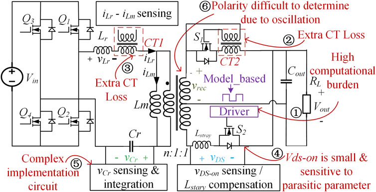
FIGURE 1. Conventional SR driving schemes: ① for sensorless model-based method, ②, ③for current sensing, ④ for VDS-on sensing, and ⑤, ⑥ for high-voltage sensing.
The first category of SR driving strategies is the sensorless model-based method. Zhu et al. (2021) built a mathematical model to determine that the turn-on instant and conduction time are adjusted adaptively. Li et al. (2021) built mathematical models based on the LLC equivalent impedance to calculate the SR on-time in the forward and reverse modes. Li et al. (2022) built a mathematical model to calculate the SR conduction time online in the forward and reverse modes and to determine the SR turn off instant considering the switching frequency and load. These schemes can modulate the SR control signal with high accuracy in the steady state. These solutions can reduce the cost by eliminating additional sensors; however, the theoretical models of these schemes are complex, leading to a high computational burden on the controller.
The second category is based on detecting primary or secondary side currents. A method to directly drive the SR based on the secondary current is proposed in Xie et al. (2001). The advantage of the direct driving strategy its simplicity and accuracy, and the strategy can be used in different working modes without additional driving power. In Kim et al. (2012), an SR scheme based on the primary side current drive of the transformer is introduced. By generating an auxiliary current source, the magnetizing current (
The third category of the existing technology is the
One method is to use an RC circuit to compensate for the stray inductance. Fu et al. (2009) used resistors, capacitors, and switches, and the conduction of the SR body diode was almost 0. A compensation circuit based on resistors, capacitors, and diodes was proposed by Wang et al. (2010) and Wang and Liu (2014), which can realize the compensation function more reliably and simply. However, this method needs to obtain an accurate SR parasitic inductance value to set the RC compensation circuit. At the same time, the compensation circuit may require a small switch MOS, which will increase the complexity of the system.
Another method is the use of an adaptive control strategy. The method was introduced by Qian et al. (2022) to improve reverse current. Moon et al. (2019) proposed an adaptive control method based on the last dead time measurement to realize the SR function. Measurement of dead time and a high-speed controller are also needed. The method proposed in Fei et al. (2018) is synchronized with the primary side, in which the switch-on point is at the primary side’s turn-on time, and the switch-off point is based on the automatic adjustment process. The main advantage of this method is that it reduces the controller requirements through ripple measurement. These methods may introduce system reliability issues, which may lead to shoot-through. MOS changes in on-time may also introduce loss.
The last category is the high-voltage sensing method. In Hsu et al. (2019), the synchronous rectification function is realized by integrating and comparing the resonant capacitor voltage (
To resolve the aforementioned challenges of LLC converters, an SR strategy for LLC resonant converters based on the resonant inductor voltage (
The principle of this method is shown in Figure 2. This method can judge the working stage of the LLC resonant converter by measuring the value of the resonant inductor voltage (
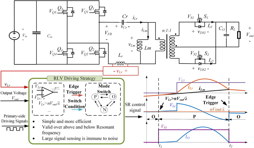
FIGURE 2. Proposed RLV strategy senses large voltage signals.
The proposed RLV strategy can turn on the SR MOS accurately and quickly and improve the conversion efficiency of the LLC converter. The inductor voltage
Section 2 describes the detailed steps of operations, which demonstrate that the RLV method covers a wide operating range of frequencies from below to above and loads from heavy to light. The realization of a driving strategy based on RLV-SR is also introduced in this section. In Section 3, experimental results are presented to verify the effectiveness of the proposed RLV method. The conclusion is provided in Section 4.
2 RLV-SR driving strategy
To illustrate this method, the LLC topology circuit is shown in Figure 2. A full-bridge structure is adopted for the inverter part, and the rectifier part is a half-bridge structure. The system inverter part Q1/Q4 is a group of identical signals, and Q2/Q3 is a group of identical signals, which are sent out by the controller as known signals.
The implementation of the proposed driving scheme is shown in Figure 3. The resonant inductor voltage
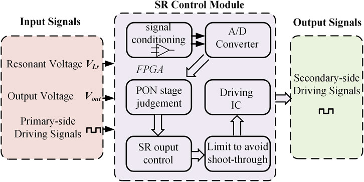
FIGURE 3. Key implementation of the proposed driving scheme.
The FPGA module uses the RLV-SR strategy to determine the PON stage according to
Before the SR drive signals are output, some output limits are set to avoid MOS shoot-through. When the upper and lower transistors of the SR signal are turned on, a dead time is set to prevent the MOS from being shoot-through. At the same time, when
For LLC converters, according to the relationship between the current
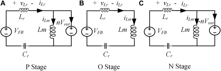
FIGURE 4. Three operation stages for the LLC resonant converter. (A) P stage. (B) N stage. (C) O stage.
If
If
The RLV-based SR signal needs to be completed through the following steps.
Step 1:. Measure the resonant inductor Lr voltage
Step 2:. Judge the working stage of the LLC converter according to the value of
Step 3:. Measure the duration of the P stage (
Step 4:. Using the current working stage obtained in Step 2 and the duration of each stage measured in Step 3, under the condition that the system output voltage is stable and the system output frequency is stable, output the synchronous rectification signals
2.1 Below resonant frequency region
When the operating frequency (
(1) The controller measures the resonant inductor vLr in real time, and the falling edge time of the control signal
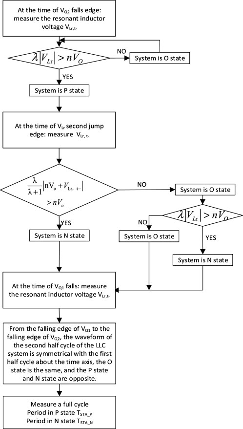
FIGURE 5. Flow chart of the RLV-SR strategy algorithm for below resonance.
If the system meets condition (1) before
(2) At the time of the rising edge of the control signal
(3) Continue to judge condition (1), if
(4) After the system enters the P state, by measuring the resonant inductor Lr voltage
If it is converted from the P state to the O state, calculate the voltage
If the calculated value
(5) If the system is at the O stage, the next stage will be the N stage. By measuring the resonant inductor Lr voltage
(6) If the system is converted to the N state, this state remains until the end of the first half cycle, and the end time is the control signal
(7) From the time of the falling edge of
As shown in Figure 6, the waveform of the lower half cycle of the LLC system is symmetrical with the upper half cycle about the time axis, and the O state is the same, while the P state and N state are opposite.
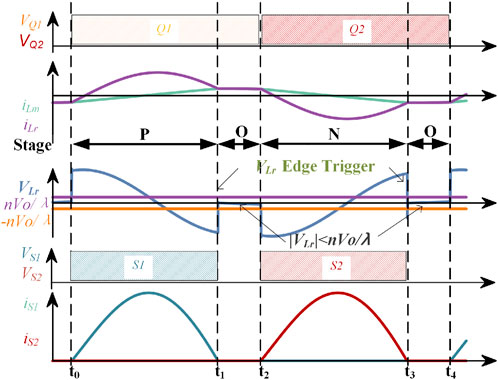
FIGURE 6. Key waveform of the RLV scheme for below resonance.
The specific algorithm flow chart of the RLV-SR strategy algorithm for below resonance is shown in Figure 5.
Since the real-time status of the system can be measured by the aforementioned method, the P stage and N stage duration time can be measured synchronously.
2.2 Above resonant frequency region
When
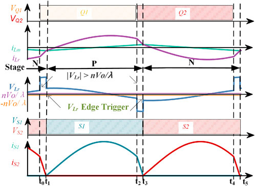
FIGURE 7. Key waveform of the RLV scheme for above resonance.
From the time of the falling edge of
(1) The controller measures the resonant inductor
If the system meets condition (1) before
(2) At the time of the rising edge of the control signal
(3) Continue to judge condition (1). If
(4) After the system enters the N state, by measuring the resonant inductor Lr voltage
If it is converted from the P state to the O state, calculate the voltage
If the calculated value
(5) If the system is at the O stage, the next stage will be the P stage. By measuring the resonant inductor Lr voltage
(6) If the system is converted to the P state, this state remains until the end of the first half cycle, and the end time is the control signal
(7) From the time of the falling edge of
The flow chart of the RLV-SR strategy algorithm for above resonance is similar to the one shown in Figure 5.
As shown in Figure 7, the waveform of the lower half cycle of the LLC system is symmetrical with the upper half cycle about the time axis, and the O state is the same, while the P state and N state are opposite. Since the real-time stage can be measured by the aforementioned method, the P stage and N stage duration time can be measured synchronously.
2.3 Light-load condition
When the system works in a light-load condition, it is divided into below and above resonant frequency zones, as shown in Figure 8.
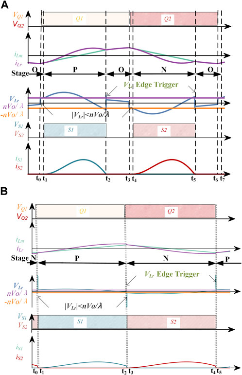
FIGURE 8. Key waveform of the RLV scheme for light-load condition: (A) below resonance and (B) above resonance.
The situation below the resonant frequency with light-load condition is shown in Figure 8A. At time
During
During
During the second half cycle of
The situation above the resonant frequency with light load is shown in Figure 8B. During
During
It can be seen from the aforementioned analysis that the state of the system changes from N to P in the first half cycle.
During the second half cycle of
3 Experimental results
This section presents the experimental results of the proposed RLV strategy based on Table 1. This 100-W/24-V LLC converter is used to provide isolation for single-board power supplies. The RLV-SR strategy is compared with the conventional
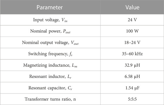
TABLE 1. Parameters of the LLC resonant converter.
The experimental converter is shown in Figure 9. A full-bridge inverter on the primary side is controlled by the DSP controller. The RLV-SR control function is completed by the FPGA controller, and the driving signal of the SR is determined by collecting
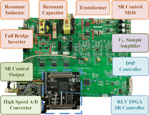
FIGURE 9. Experimental prototype: 100-W/24V resonant converter based on the RLV-SR control strategy.
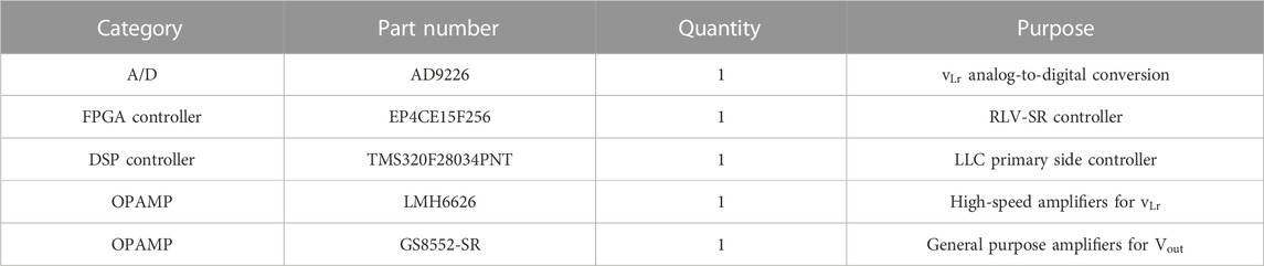
TABLE 2. Parameters of the SR controller.
Four voltage signals were given in the experimental result figures. While
In the below resonant frequency region, the converter operates at the same load and frequency, the results of the conventional
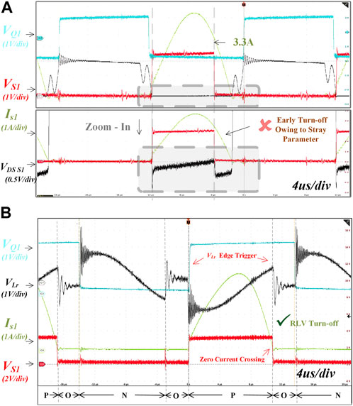
FIGURE 10. Experimental results below resonant frequency at the maximum power, 100 W/36 kHz. (A) VDS-ON measurement method shuts down the SR early since the
As shown in the bottom part of Figure 10A,
Unlike the conventional
In the operating range above the resonant frequency, when the converter operates under the same load and frequency, the conventional
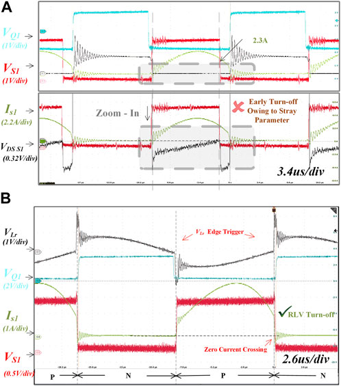
FIGURE 11. Experimental results of above resonant frequency at the maximum current, 3A/58 kHz. (A) The
When the operating frequency (
It can be seen in the upper part of Figure 11A that
As shown in Figure 11B, when the converter operates in a mode above the resonant frequency, the RLV strategy effectively determines the zero-current crossing point by detecting the jump edge of
When the load of the converter is light, the output power of the system is 20 W, and the system works at 36 kHz. The experiment results are shown in Figure 12. The traditional
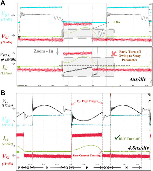
FIGURE 12. Experimental results at a light-load mode below resonant frequency, 20 W/36 kHz. (A) The
As shown in Figure 12A, the conventional
On the contrary, with the RLV-based strategy, the system state can be accurately judged by the magnitude and jump edge of the
The RLV-SR strategy tracks the actual rectifier current conduction time instantaneously under severe current dynamics. The input voltage of the experimental system is fixed. Therefore, the dynamic response results are shown while the load is changed dramatically. The results when the load condition steps up from 20 W to a load of 66 W are shown in Figure 13A. In the figure, IS1 represents the output current, and VS1 represents the driving signal of SR MOS. There are no spikes in the dynamic waveforms, which means the SRs can operate safely. To regulate the output voltage, the S1 peak current steps up from 3.8 A to 12 A. Figure 13B shows the load step-down response from 62 W to 20 W with a step-up increase in S1 peak current from 3.8 A to 12 A. The zoomed-in figure shows the waveforms after transients. It can be seen that the conducting time of SR can be tracked properly during the transients with the proposed driving scheme.
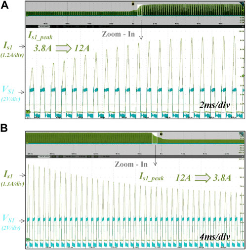
FIGURE 13. Dynamic test waveforms under a large load change: (A) Is1_peak from 3.8 A to 12 A and (B) Is1_peak from 12 A to 3.8 A.
The experimental results verify that the RLV-based synchronous rectification strategy can effectively cover the operating range from below to above the resonant frequency and can also cover the working scenarios from light load to heavy load. Compared with the conventional
A comparison of the different schemes is shown in Table 3. The proposed RLV strategy does not require current sensors, which may introduce volume and cost issues. Although the proposed strategy contains one voltage sensor, it shows excellent performance in low extra power losses, low noise sensitivity, and low circuit, resulting in high SR accuracy and high efficiency. To summarize, the proposed SR scheme achieves better performance than most of the existing SR schemes of the LLC resonant converter to some extent.
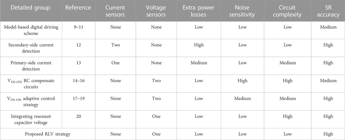
TABLE 3. Comparison of different driving schemes.
As shown in Figure 14, the converter achieves a peak efficiency of 92.45% with an improvement of 0.5% at 50 W compared to the conventional driving scheme because the current over zero point can be determined by detecting the jump edge of VLR and the operating state of the system.
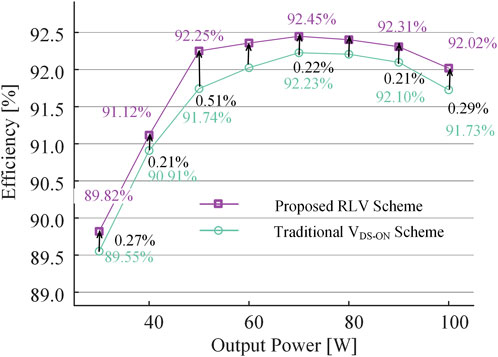
FIGURE 14. Comparison of driving scheme efficiency.
4 Conclusion
In this paper, an RLV-SR strategy is proposed. This RLV-SR strategy does not use a current sensor, and the working stage of the LLC converter is judged by measuring the magnitude and jump time of the
Compared with the conventional
Therefore, the RLV-SR strategy proposed in this paper is a simple and effective method to realize the synchronous rectification function of the LLC resonant converter.
Data availability statement
The original contributions presented in the study are included in the article/Supplementary Material; further inquiries can be directed to the corresponding author.
Author contributions
ZL: writing—original draft and review. ZW and XQ: conceptualization. XX, XD, and QH: formal analysis and revision.
Conflict of interest
The authors declare that the research was conducted in the absence of any commercial or financial relationships that could be construed as a potential conflict of interest.
Publisher’s note
All claims expressed in this article are solely those of the authors and do not necessarily represent those of their affiliated organizations, or those of the publisher, the editors, and the reviewers. Any product that may be evaluated in this article, or claim that may be made by its manufacturer, is not guaranteed or endorsed by the publisher.
References
Ahmed, M. H., de Rooij, M. A., and Wang, J. (2019). High-power density, 900-W LLC converters for servers using GaN FETs: Toward greater efficiency and power density in 48 V to 6\/12 V converters. IEEE Power Electron. Mag. 6, 40–47. doi:10.1109/MPEL.2018.2886106
Fei, C., Li, Q., and Lee, F. C. (2018). Digital implementation of adaptive synchronous rectifier (SR) driving scheme for high-frequency LLC converters with microcontroller. IEEE Trans. Power Electron. 33, 5351–5361. doi:10.1109/TPEL.2017.2731942
Fu, D., Liu, Y., Lee, F. C., and Xu, M. (2009). A novel driving scheme for synchronous rectifiers in LLC resonant converters. IEEE Trans. Power Electron. 24, 1321–1329. doi:10.1109/TPEL.2009.2012500
Hsu, J.-D., Ordonez, M., Eberle, W., Craciun, M., and Botting, C. (2019). LLC synchronous rectification using resonant capacitor voltage. IEEE Trans. Power Electron 34, 10970–10987. doi:10.1109/tpel.2019.2900459
Kim, B.-C., Park, H.-S., Moon, S. C., Kim, Y.-D., Kim, D.-Y., and Moon, G.-W. (2012). “The novel synchronous rectifier driving method for LLC series resonant converter,” in Iecon 2012 - 38th annual conference on IEEE industrial electronics society (Montreal, QC, Canada), 810–813. doi:10.1109/IECON.2012.6388647
Lee, J.-B., Kim, J.-K., Baek, J.-I., Kim, J.-H., and Moon, G.-W. (2016). Resonant Capacitor <sc>O</sc>n/<sc>O</sc>ff Control of Half-Bridge <italic>LLC</italic> Converter for High-Efficiency Server Power Supply. IEEE Trans. Ind. Electron. 63, 5410–5415. doi:10.1109/TIE.2016.2558481
Li, H., Wang, S., Zhang, Z., Zhang, J., Li, M., Gu, Z., et al. (2021). Bidirectional synchronous rectification on-line calculation control for high voltage applications in SiC bidirectional LLC portable chargers. IEEE Trans. Power Electron. 36, 5557–5568. doi:10.1109/TPEL.2020.3027703
Li, H., Wang, S., Zhang, Z., Zhang, J., Zhu, W., Ren, X., et al. (2022). An impedance-based digital synchronous rectifier driving scheme for bidirectional high-voltage SiC LLC converter. IEEE Trans. Ind. Electron. 69, 11314–11323. doi:10.1109/TIE.2021.3127037
Lin, J.-Y., Yueh, H.-Y., Lin, Y.-F., and Liu, P.-H. (2023). Variable-frequency and phase-shift with synchronous rectification advance on-time hybrid control of LLC resonant converter for electric vehicles charger. IEEE J. Emerg. Sel. Top. Ind. Electron. 4, 348–356. doi:10.1109/JESTIE.2022.3176206
Mohammadi, M., and Ordonez, M. (2019). Synchronous rectification of LLC resonant converters using homopolarity cycle modulation. IEEE Trans. Ind. Electron. 66, 1781–1790. doi:10.1109/tie.2018.2840493
Moon, S. C., Chen, C., and Park, D. (2019). “Adaptive dead time synchronous rectification control for high efficiency LLC resonant converter,” in 2019 IEEE applied power electronics conference and exposition (APEC) (Anaheim, CA, USA: IEEE), 2939–2946. doi:10.1109/APEC.2019.8721896
Qian, Q., Liu, Q., Zheng, M., Zhou, Z., Xu, S., and Sun, W. (2022). An improved adaptive synchronous rectification method with the enhanced capacity to eliminate reverse current. IEEE Trans. Power Electron. 37, 1–1410. doi:10.1109/TPEL.2021.3106477
Tayebi, S. M., Hu, H., Abdel-Rahman, S., and Batarseh, I. (2019). Dual-input single-resonant tank LLC converter with phase shift control for PV applications. IEEE Trans. Ind. Appl. 55, 1729–1739. doi:10.1109/TIA.2018.2883015
Wang, D., Jia, L., Fu, J., Liu, Y.-F., and Sen, P. C. (2010). “A new driving method for synchronous rectifiers of LLC resonant converter with zero-crossing noise filter,” in 2010 IEEE energy conversion congress and exposition (Atlanta, GA: IEEE), 249–255. doi:10.1109/ECCE.2010.5618032
Wang, D., and Liu, Y.-F. (2014). A zero-crossing noise filter for driving synchronous rectifiers of LLC resonant converter. IEEE Trans. Power Electron. 29, 1953–1965. doi:10.1109/TPEL.2013.2264774
Wang, X., Jiang, C., Lei, B., Teng, H., Bai, H. K., and Kirtley, J. L. (2016a). Power-loss analysis and efficiency maximization of a silicon-carbide MOSFET-based three-phase 10-kW bidirectional EV charger using variable-DC-bus control. IEEE J. Emerg. Sel. Top. Power Electron. 4, 880–892. doi:10.1109/JESTPE.2016.2575921
Wang, Y., Gao, S., Guan, Y., Huang, J., Xu, D., and Wang, W. (2016b). A single-stage LED driver based on double LLC resonant tanks for automobile headlight with digital control. IEEE Trans. Transp. Electrification 2, 357–368. doi:10.1109/tte.2016.2571781
Xie, X., Liu, J. C. P., Poon, F. N. K., and Pong, M. H. (2001). A novel high frequency current-driven synchronous rectifier applicable to most switching topologies. IEEE Trans. Power Electron. 16, 635–648. doi:10.1109/63.949496
Yang, C.-H., Liang, T.-J., Chen, K.-H., Li, J.-S., and Lee, J.-S. (2013). “Loss analysis of half-bridge LLC resonant converter,” in 2013 1st international future energy electronics conference (IFEEC) (Tainan, Taiwan: IEEE), 155–160. doi:10.1109/IFEEC.2013.6687496
Zhang, J., Shao, S., Li, Y., Zhang, J., and Sheng, K. (2021). A voltage balancing method for series-connected power devices in an LLC resonant converter. IEEE Trans. Power Electron. 36, 3628–3632. doi:10.1109/TPEL.2020.3025595
Keywords: LLC resonant converter, resonant inductor voltage, driving strategy, synchronous rectification, DC–DC converters
Citation: Luo Z, Wu Z, Quan X, Xie X, Dou X and Hu Q (2023) Synchronous rectification of LLC resonant converters based on resonant inductor voltage. Front. Energy Res. 11:1199397. doi: 10.3389/fenrg.2023.1199397
Received: 03 April 2023; Accepted: 06 June 2023;
Published: 29 June 2023.
Edited by:
Tao Xu, Shandong University, ChinaReviewed by:
Qinglei Bu, Xi’an Jiaotong-Liverpool University, ChinaLiansong Xiong, Xi’an Jiaotong University, China
Copyright © 2023 Luo, Wu, Quan, Xie, Dou and Hu. This is an open-access article distributed under the terms of the Creative Commons Attribution License (CC BY). The use, distribution or reproduction in other forums is permitted, provided the original author(s) and the copyright owner(s) are credited and that the original publication in this journal is cited, in accordance with accepted academic practice. No use, distribution or reproduction is permitted which does not comply with these terms.
*Correspondence: Zaijun Wu, emp3dUBzZXUuZWR1LmNu