 Wenping Zhang
 Donghui Li
 Yiming Wang2
- 1School of Electrical and Information Engineering, Tianjin University, Tianjin, China
- 2Research Center, Ginlong Technologies Co., Ltd., Ningbo, China
In large PV plants, a large number of PV inverters are linked together at grid-side to generate more power. However, as the number of PV inverter modules increases, the ground current problem worsens. This can result in a ground current fault, and cause the inverter failed and disconnected from the grid. In this paper, the solutions, including hardware and software, are proposed to suppress the ground current. The hardware solution is to connect filter capacitors back to the DC-bus, directing more ground current to the inverter rather than the grid to reduce the ground current. Additionally, the software solutions, including carrier phase shifting and carrier frequency shifting, are proposed. In the software solutions, the ground current for PV inverters can be cancelled each other, which can alleviate the ground current problem. In the paper, the system architecture is presented first. The concept of connecting the neutral point of the filter capacitors to the DC-bus midpoint is explained. The zero-sequence mathematical model is then built. Moreover, the effect of the zero-sequence voltages of the DC/AC converter and the grid on the zero-sequence current is investigated. Then, the hardware solution is explained. The control architecture is presented, followed by an explanation of how to obtain the three-phase output voltage and zero-sequence components for PV inverters. Two software solutions, including carrier phase shifting and carrier frequency shifting, are detailed. Finally, the experiment is conducted to verify the theory.
1 Introduction
With the increasing severity of environmental pollution and energy crisis, developing and utilizing renewable energy has become a top priority (Zhang et al., 2023a). As a result, photovoltaic generation has received a lot of attention in recent years, and grid-connected inverters are widely used for energy conversion (Xu et al., 2023). To maximize power generation efficiency in PV systems, MPPT technology is widely used to track maximum power point of PV strings (Ranjan Satpathy et al., 2024a)- (Ranjan Satpathy et al., 2024b). However, when PV modules are blocked to varying degrees, the power curve will have multiple peaks; thus, numerous improved MPPT algorithms are proposed to improve system power tracking efficiency. At the same time, the topology of grid-connected inverters has direct impact on energy conversion efficiency. Different topology structures are proposed to improve switching losses, EMI suppression, common mode voltage, and so on (Azizi et al., 2025). Grid-connected inverters can be divided into two types based on their topology: isolated and non-isolated. Transformerless non-isolated grid-connected inverters are ideal for photovoltaic grid-connected systems due to their small size, low costs, and simple structure, as well as their high efficiency (Azizi et al., 2025)- (Sharma et al., 2023). As a result, an increasing number of PV grid-connected inverters are adopting non-isolated topologies. However, in the absence of the electrical isolation function, the system can generate a large ground current due to inverter and PV parasitic capacitors connected to the ground. Ground current can increase system losses while also posing safety and electromagnetic compatibility concerns. In recent years, academics have conducted extensive research on ground current suppression technology (Anand et al., 2023)- (Gyawali et al., 2024). The main idea is to create a new freewheeling path between the photovoltaic and AC grid sides. As a result, the common-mode voltage is held constant. The ground current can be reduced when the common-mode voltage remains constant. The following are some examples of typical topology modifications based on this concept.
For single-phase full-bridge topology, there are numerous modifications. H5 topology is one of them (Xiao et al., 2011). The H5 topology, as shown in Figure 1a, adds an additional switch SDC in series at the DC input. The additional switch allows for the decoupling of the AC and DC sides, which suppresses ground current. However, because SDC is always operated at high frequencies, it withstands high switching losses. There is another H5 variant (Tofigh Azary et al., 2018), which is shown in Figure 1b. In comparison to H5 topology, the switch SDC is divided into two (SDC1 and SDC2). As a result, the original SDC loss can be shared by SDC1 and SDC2. This can make heat dissipation design less difficult. Another typical topology modification is Highly Efficient Reliable Inverter Concept (HERIC) (Gonzalez et al., 2007)- (Xiao et al., 2014). On the AC side, the HERIC topology adds a freewheeling circuit consisting of two switches (Sac1, Sac2), as shown in Figure 1c. In comparison to H5, the number of conducting devices is always two, resulting in a lower conduction loss. As a result, the device loss distribution is more balanced, potentially extending the device lifetime. The main disadvantage is that the costs are relatively high. Figure 1d depicts the topology of H6 (Ji et al., 2013)- (Liu et al., 2017). Based on the traditional full-bridge topology, this topology adds switches S5 and S6 as well as diodes D1 and D2. These additional switches provide a freewheeling path. Then, the DC side can be disconnected from the grid to suppress common-mode voltage. The benefit of this topology is that the voltage stress of the devices is reduced to 1/2 of the DC-bus voltage, effectively reducing switching loss. The main disadvantage remains the additional costs.
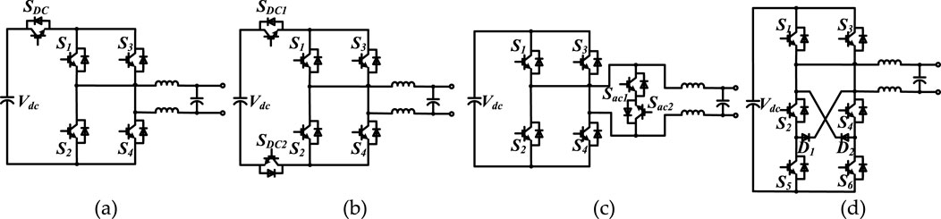
Figure 1. Full-bridge topology modifications, (a) H5 topology; (b) H5 variant; (c) HERIC topology; (d) H6 topology.
For the modulation, unipolar, bipolar, and frequency doubling unipolar are typically used in single-phase full-bridge topology (Mohon et al., 1995)- (Holmes and Lipo, 2003). The common-mode voltage for unipolar and frequency doubling unipolar modulations varies between 0 and Vdc. Contrarily, with bipolar modulation, the common-mode voltage is a constant of Vdc/2 and the ground current is 0. Therefore, the bipolar modulation is frequently employed in single-phase full-bridge topology in order to suppress ground current.
For half-bridge topologies or three phase topologies with three half-bridges, a common method to suppress ground current is to connect the grid to the DC-bus’s midpoint. Because the DC-bus capacitors are relatively large, they can provide a low impedance path for the ground current. This allows the majority of the ground current to flow into the DC-bus. As a result, the ground current flowing into the earth can be greatly reduced. In high-power applications, multi-level inverters are frequently used to improve output waveform quality, reduce switching stress, and lower electromagnetic interference levels (Azizi et al., 2025). For typical 1500V PV systems, 3-level topologies are widely adopted. The three-level inverters differ from traditional two-level inverters in that it has an additional intermediate voltage level known as zero level. Figure 2a presents the neutral-point clamped (NPC) topology. The zero level is connected to the midpoint of the DC bus via a diode, improving output voltage control and system power quality (Nabae et al., 1981)- (Barzegarkhoo et al., 2023). It is known that the outer switches (S1 and S4) operate at a high frequency, resulting in high switching losses. In contrast, the inner switches (S2 and S3) operate at a low switching frequency, with low switching losses. As a result, in long-term operation, the loss distribution is uneven, which affects device reliability. In order to solve the problem of uneven distribution of device losses, Active NPC (ANPC) topology is proposed, as shown in Figure 2b (Barzegarkhoo et al., 2023). Furthermore, T-type 3-level are also widely adopted as shown in Figure 2c. This topology features higher efficiency in medium switching frequency (Zhang et al., 2023c)- (Zhang et al., 2024). Although 3-level topologies described above are widely used in PV systems, they have limitations in terms of ground current suppression (Barzegarkhoo et al., 2023). It is worth noting that this ground current suppression method requires grid neutral-point accessibility. A novel 3-phase H8 architecture is proposed by adding two additional switches in the DC path that allow decoupling the AC side from the DC side during freewheeling phases (Noroozi et al., 2017)- (Concari et al., 2017). Furthermore, optimized modulation strategies are explained.
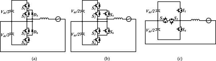
Figure 2. Half-bridge topology, (a) NPC topology; (b) ANPC topology; (c) T-type.
In practice, 3-wire systems are widely used for 3-phase PV systems. This means that the grid neutral-point cannot be accessed and thus cannot be connected to the dc-bus. In this case, it is common ground current suppression practice to increase the inverter’s capacitors to ground. However, this comes at a higher cost, and the suppression effect is not perfect. Furthermore, in large PV plants, a large number of PV inverters are linked together at the grid-side to generate more power. As the number of PV inverter modules increases, the ground current problem worsens. This can easily result in a ground current fault, and cause the inverter system failed and disconnected from the grid. Therefore, this paper will propose solutions for reducing ground current in 3-phase systems with a large number of PV inverter modules. The hardware solution is to connect filter capacitors back to the DC-bus, directing more ground current to the inverter rather than the grid to reduce the ground current. The software solutions include carrier phase shifting and carrier frequency shifting. The ground current for the PV inverter modules can be cancelled each other in software solutions, which can alleviate the ground current problem.
The following are the main contributions of this paper.
1) The concept of connecting neutral point of filter capacitors to DC-bus midpoint to suppress ground current is introduced. The effects of the DC/AC converter’s zero-sequence voltage and the grid’s zero-sequence voltage on zero-sequence current are investigated.
2) A hardware solution is proposed to suppress ground current. When the zero-sequence current is primarily caused by the DC/AC converter’s zero-sequence voltage, increasing the value of capacitors connected to DC-bus can reduce ground current. When the zero-sequence voltage is primarily from the grid side, increasing the value of capacitors connected to the grid neutral point can reduce ground current.
3) Two software solutions, carrier phase shifting and carrier frequency shifting, are proposed to suppress ground current, particularly in systems with a large number of PV inverter modules. The concept and implementation for two proposed software solutions are detailed.
It is worth mentioning that the proposed hardware solution simply connects filter capacitors to the dc-bus or the grid neutral point to suppress ground current, which is significantly less expensive than adding additional switching devices. Furthermore, the software solution, which is intended for multi-inverter parallel scenarios, uses phase shifting and frequency staggering of the carrier to effectively suppress ground currents without incurring additional hardware costs.
2 System architecture and zero-sequence model
The system architecture is presented in Figure 3. PV feeds the grid via DC/AC converters. The DC/AC converter uses 3-level NPC topology, but not limited to it. In Figure 3, there are three ground capacitors. CPV+ and CPV- represent the capacitors of the PV to the ground; Cdc+ and Cdc- represent the capacitors of the DC-bus to the ground; and Cac represents the capacitor of the output filter to the ground. The output zero-sequence current i0 is measured, which represents the system’s ground current.
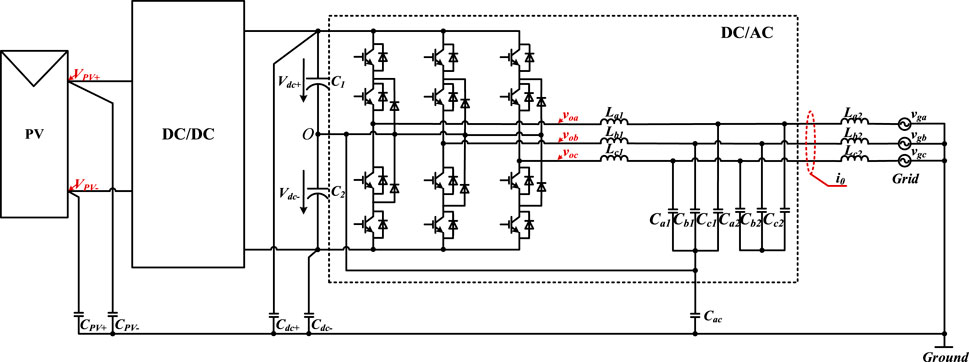
Figure 3. System architecture.
In the architecture, the output filter capacitors are divided into two groups. Ca1, Cb1 and Cc1 are in one group, while Ca2, Cb2 and Cc2 are in the other group. The distinction is whether the neutral point of the filter capacitors is connected to the DC-bus midpoint. By connecting the filter capacitors (Ca1, Cb1 and Cc1) to the DC-bus, a portion of the zero-sequence current from the inverter-side can flow into the DC-bus, which can reduce the ground current flowing into the grid-side.
Assume that the DC/AC converter’s output voltages with respect to the DC-bus neutral point O are voa, vob, and voc. Furthermore, the PV positive and negative with respect to the DC-bus neutral point O are VPV+ and VPV-, respectively. The equivalent mathematical model is obtained and illustrated in Figure 4a.
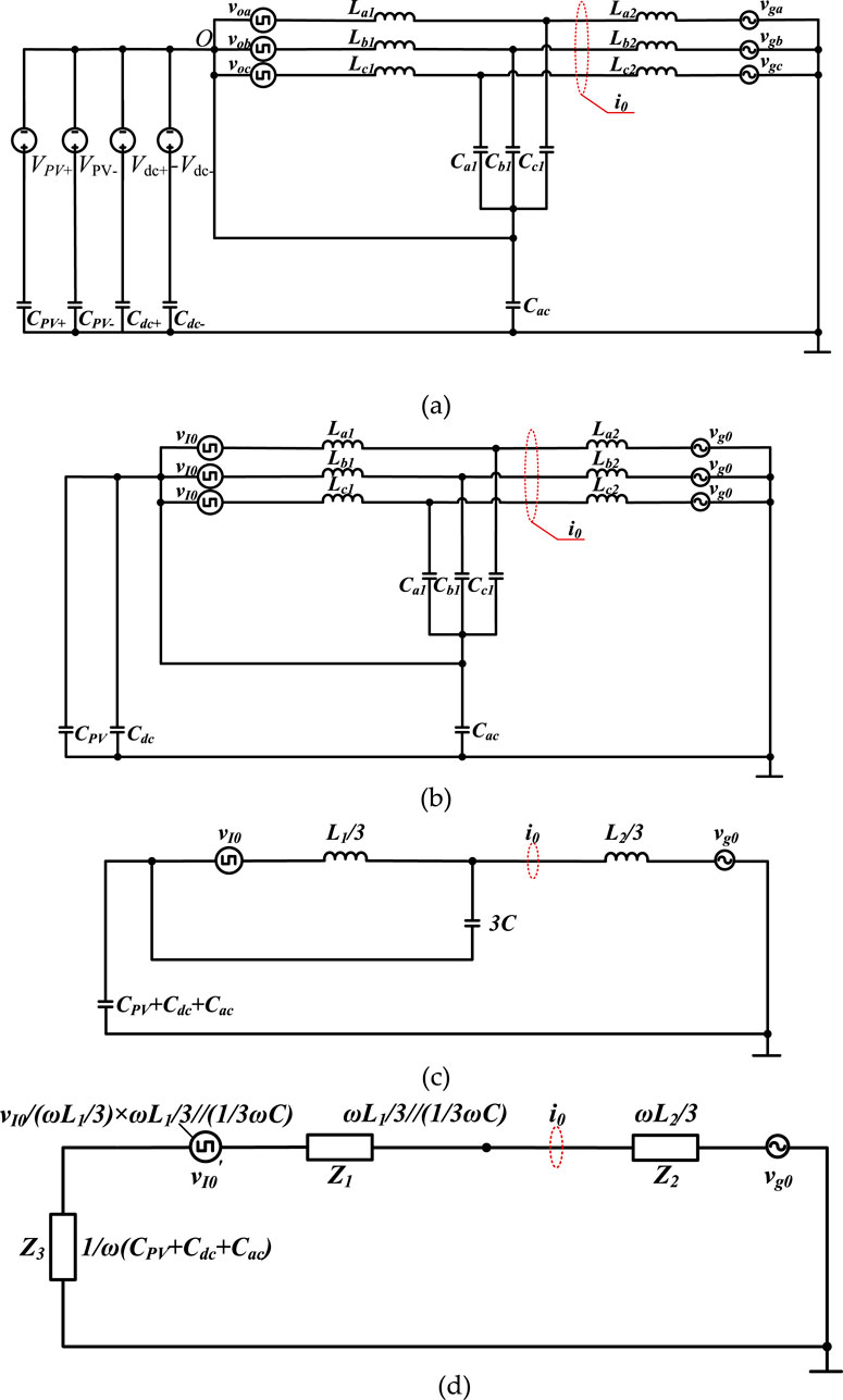
Figure 4. Zero-sequence model, (a) equivalent model; (b) simplified model; (c) further simplified model; (d) impedance model.
Because ground current is proportional to zero-sequence voltage, the zero-sequence equivalent circuit is investigated. Assume the DC/AC converter’s output zero-sequence voltage is vI0 and the grid’s zero-sequence voltage is vg0. Furthermore, assuming that Vdc+ = Vdc- = Vdc/2, VPV+ = –VPV-, CPV+ = CPV- = CPV/2, and Cdc+ = Cdc- = Cdc/2, Figure 4a can be simplified to Figure 4b.
Due to the symmetry of the parameters La1 = Lb1 = Lc1 = L1, La2 = Lb2 = Lc2 = L2 and Ca1 = Cb1 = Cc1 = C, Figure 4b can be simplified to Figure 4c.
The circuit can be further simplified from Figure 4c, and the corresponding impedance model can be obtained, which is shown in Figure 4d.
3 Zero-sequence current analysis
Based on Figure 4, the following will investigate the effect of the DC/AC converter’s zero-sequence voltage vI0 and the grid’s zero-sequence voltage vg0 on zero-sequence current i0.
3.1 Effect of DC/AC converter’s zero-sequence voltage on zero-sequence current
First, by setting the grid zero-sequence voltage vg0 to zero, examine the effect of the DC/AC converter’s zero-sequence voltage vI0 on the zero-sequence current i0. From Figure 4d, the expressions for
From Figure 4d, the zero-sequence current i0 can be obtained as well. Table 1 shows the system parameters. With the parameters and Table 1, the zero-sequence current i0 can be calculated.
Table 1. System parameters.
Figure 5 shows bode diagram for the zero-sequence current i0 when only vI0 exists and vg0 = 0. From Figure 5, there are two resonant frequencies. One is the resonance of L1 and C with a resonant frequency of around 5 kHz. The second is the resonance of L2 and CPV, Cdc and Cac, with a resonant frequency of around 120 kHz.
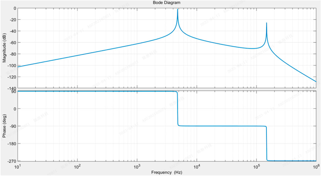
Figure 5. Bode diagram for the zero-sequence current i0 when only vI0 exists.
Figure 6 presents bode diagram for the zero-sequence current i0 in case of different filter capacitors C. From it, it can be seen that the resonant frequency shifts to the left as the value of the capacitor connected to the DC-bus increases. As a result, the zero-sequence current suppression in the high frequency band is improved. Specifically, when the capacitor connected to the DC-bus is doubled, the zero-sequence current suppression in the range of 10 kHz–100 kHz is increased by approximately 7 dB. Furthermore, taking 10 kHz as an example, when C is 1.1μF, the magnitude of i0 is −45 dB. When C is 2.2μF, the magnitude of i0 is −53dB, and when C is 4.4μF, the magnitude of i0 is further suppressed to −60 dB.
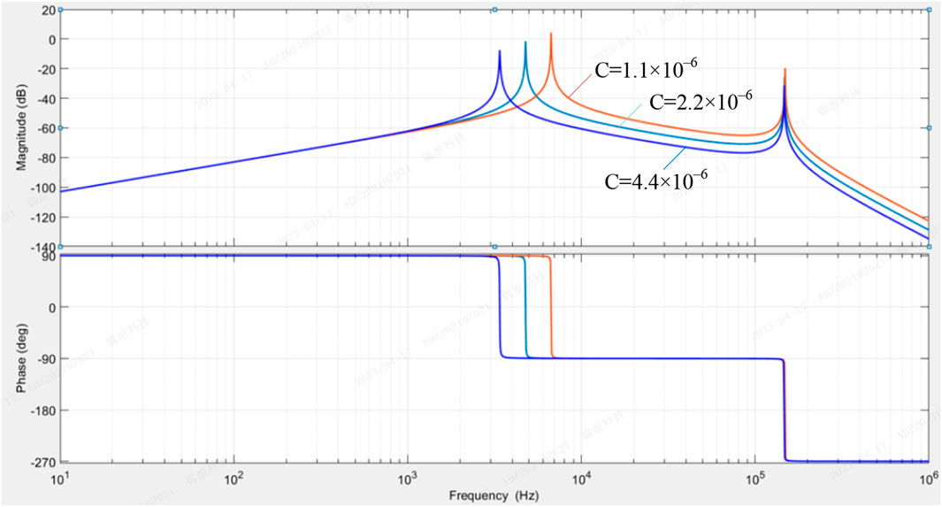
Figure 6. Bode diagram for the zero-sequence current i0 in case of different filter capacitor C when only vI0 exists.
3.2 Effect of the grid’s zero-sequence voltage on zero-sequence current
Similarly, by setting the DC/AC converter’s zero-sequence voltage vI0 to zero, examine the effect of the zero-sequence grid voltage vg0 on the zero-sequence current i0. From Figure 4c, the zero-sequence current i0 can be obtained as well.
With the parameters in Table 1 and Equation 5, the zero-sequence current i0 can be calculated. Figure 7 shows bode diagram for the zero-sequence current i0 when only vg0 exists and vI0 = 0. From Figure 7, there are two resonant frequencies. The first one is the resonance of L1 and C with a resonant frequency of around 5 kHz. The second one is the resonance of L2 and CPV, Cdc and Cac, with a resonant frequency of around 120 kHz. Furthermore, compared with the result in Figure 5, of these two resonators, the second resonator (∼120K) predominates in this case.
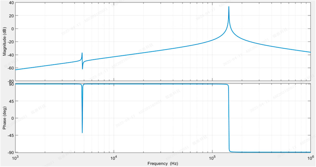
Figure 7. Bode diagram for the zero-sequence current i0 when only vg0 exists.
Figure 8 presents bode diagram for the zero-sequence current i0 in case of different filter capacitors C. From it, the first resonant frequency shifts to the left as the capacitor connected to the DC-bus C increases. Generally, there are no changes on the effect of zero-sequence current suppression. This is because, the zero-sequence current is determined by the loop impedance, and the impedance of the loop is determined primarily by the capacitors of CPV, Cdc and Cac, rather than the capacitor connected to DC-bus C.
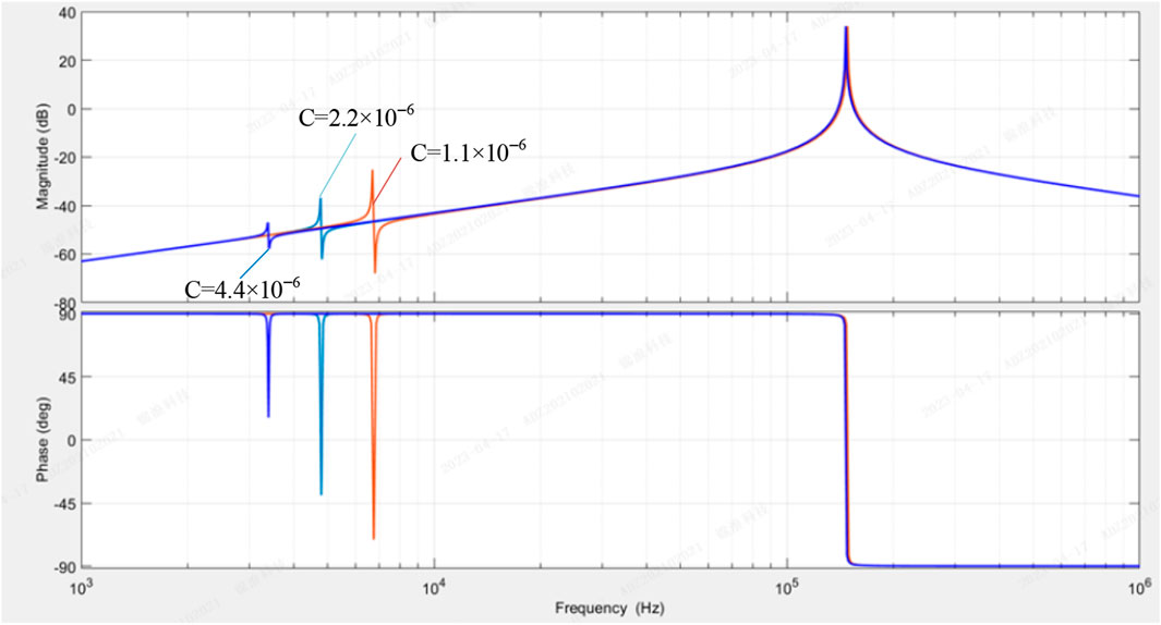
Figure 8. Bode diagram for the zero-sequence current i0 in case of different filter capacitor C when only vg0 exists.
4 Hardware solution for ground current suppression
According to the above analysis, when the zero-sequence current is caused by the DC/AC converter’s zero-sequence voltage, increasing capacitance connected to the DC-bus can greatly improve zero-sequence current suppression. When the zero-sequence current is caused by the zero-sequence grid voltage, increasing capacitance connected to DC-bus C has no effect on the zero-sequence current suppression. Therefore, when the zero-sequence voltage comes primarily from the converter side rather than the grid side, one simple way to reduce ground current is to increase the capacitance of filter capacitors connected to the DC-bus.
When the zero-sequence voltage is primarily from the grid side rather than the inverter side, installing capacitors connected to the grid neutral point is a simple way to reduce ground current. Figure 9 depicts an alternative system architecture in which the capacitors Cga1∼Cgc1 are added and connected to the grid neutral point. The capacitors Cga1∼Cgc1 can suppress the ground current caused by grid-side zero-sequence components.
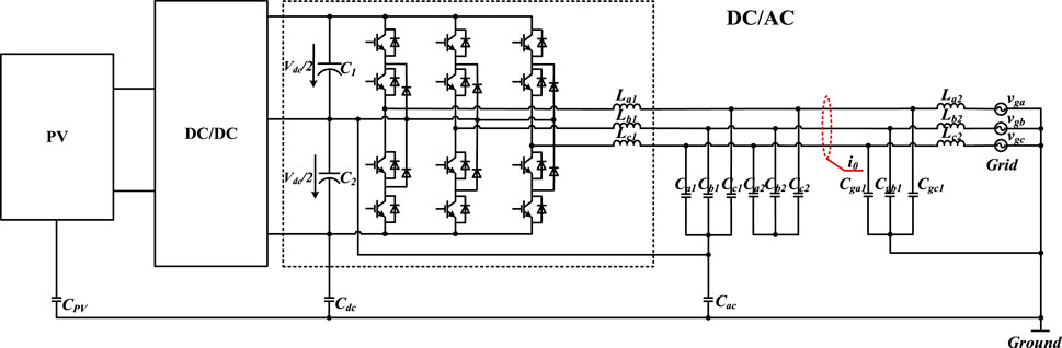
Figure 9. Hardware solution: system architecture variant I.
It is worth noting that as the capacitance of Ca1 ∼ Cc1 increases, so does the current flowing into the DC-bus, resulting in greater DC-bus fluctuation. As a result, we need make a compromise in selecting the capacitance connected to the DC-bus in order to achieve a balance between the DC-bus fluctuation and ground current. Figure 10 depicts another alternative system architecture. All filter capacitors are connected to the DC-bus midpoint or the grid neutral via a triode for alternating current (TRIAC). As shown in Figure 10, the filter capacitors (Ca1, Cb1, Cc1) are connected to the DC-bus midpoint via T1, and the filter capacitors (Cga1, Cgb1, Cgc1) are connected to the grid neutral-point via Tg1. As a result, the system has more degrees of freedom and can freely select which group of the capacitors to connect back to the midpoint of the DC-bus based on the value of the system ground current. On one hand, the ground current can be suppressed in this manner to meet the requirement; on the other hand, the impact on the DC-bus is minimal.
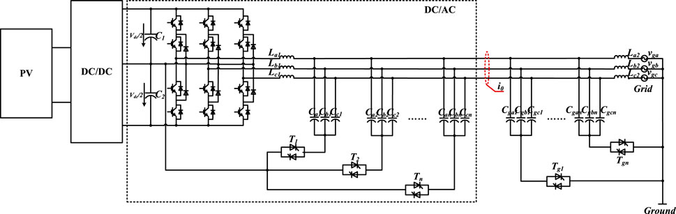
Figure 10. Hardware solution: system architecture variant II.
From the above analysis, the proposed methods for suppressing ground current are highly scalable. This approach is not limited by the inverter’s power level or the number of parallel inverters, making it particularly useful for high-power applications. The most difficult challenge is dealing with various scenarios in which ground current is caused by either the inverter or the grid. As a result, modified solutions are also proposed in the paper.
5 Software solution for ground current suppression
5.1 Control architecture
Figure 11 depicts the control architecture for the DC/AC converter in PV string systems. The outer loop is a DC-bus voltage loop, while the inner loop is a current loop. The three phases are transformed into d-q frame, and the control method is the same as the conventional one. Then, the three-phase references generated are fed into the modulation unit and cross-intercepted with the triangular wave carrier to form three-phase switching signals.
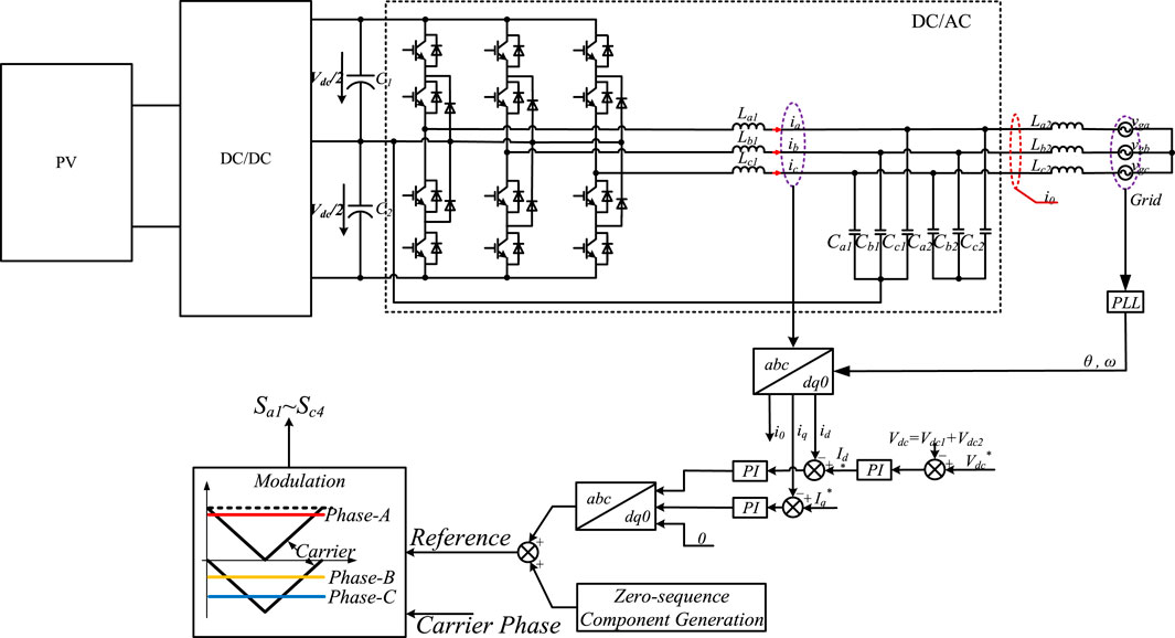
Figure 11. Control architecture.
The concept of the modulation unit is presented in Figure 12. The three-phase reference signals and triangle wave carrier are cross-sectioned, and then three-phase switching signals are obtained. As a result, three-phase output voltages (va, vb and vc) are generated, and the zero-sequence component of three-phase output voltages vcom can be calculated using (6). The three-phase output voltages and the corresponding zero-sequence component are shown in Figure 12 as well.
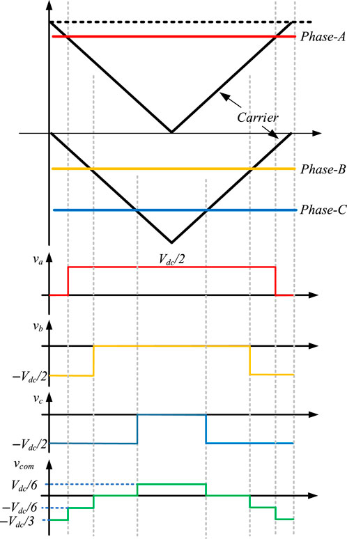
Figure 12. 3-phase references are cross-intercepted with the triangular wave carrier to form a three-phase switching signals.
The three-phase output voltage and zero-sequence components for any PV inverters can be obtained using the same method. In a large PV plant, many PV inverters are linked together at the grid-side to generate more power. Taking three PV inverter modules as an example, assuming that the voltage reference of each module is the same, the three-phase output voltages and the corresponding zero-sequence voltage components are shown in Figure 13. Using Equation 7, the sum of zero-sequence voltages for three PV inverter modules vcom_sum can be obtained, which is shown in Figure 13 as well. From Figure 13, for three PV inverter system, the maximum step of the zero-sequence voltage is Vdc/2 and the range of the change is–Vdc to Vdc/2. Also, it can be seen that as the size of the PV inverter modules increases, so do the sum of the corresponding zero-sequence voltages and the corresponding ground current. Therefore, as the number of PV inverter modules increases, the ground current may exceed the standard. This can result in a ground current fault, which can cause the inverter system failed and disconnected from the grid.
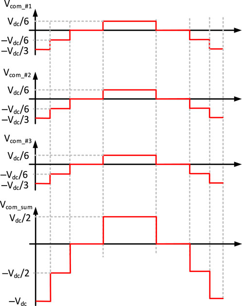
Figure 13. Zero-sequence component for three PV inverter modules.
From the above analysis, it is necessary to suppress ground current, especially for the system with high number of PV inverter modules. The following are two software solutions proposed.
5.2 Software solution I: carrier phase shifting
To suppress ground current, a triangulation wave carrier phase shifting method is proposed in this section. As shown in Figure 14, the triangle wave carrier for different inverter modules is shifted by a degree of Ø. Taking three of inverter modules as an example, when compared to module #1, the triangle wave carrier for module #2 lags by Ø, while the triangle wave carrier for module #3 is ahead by Ø.
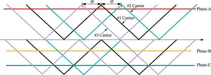
Figure 14. Carrier phase shifting method.
Figure 15 depicts the intersection of the reference signals and the phase-shifted triangle wave carriers for three inverter modules, which can result in three-phase switching signals and three-phase output voltages (va, vb, vc). Due to the fact that the triangular wave carriers for three inverter modules are phase shifted by a degree of Ø. As a result, the output voltages of three inverter modules are phase shifted by the degree of Ø, which is shown in Figure 15.
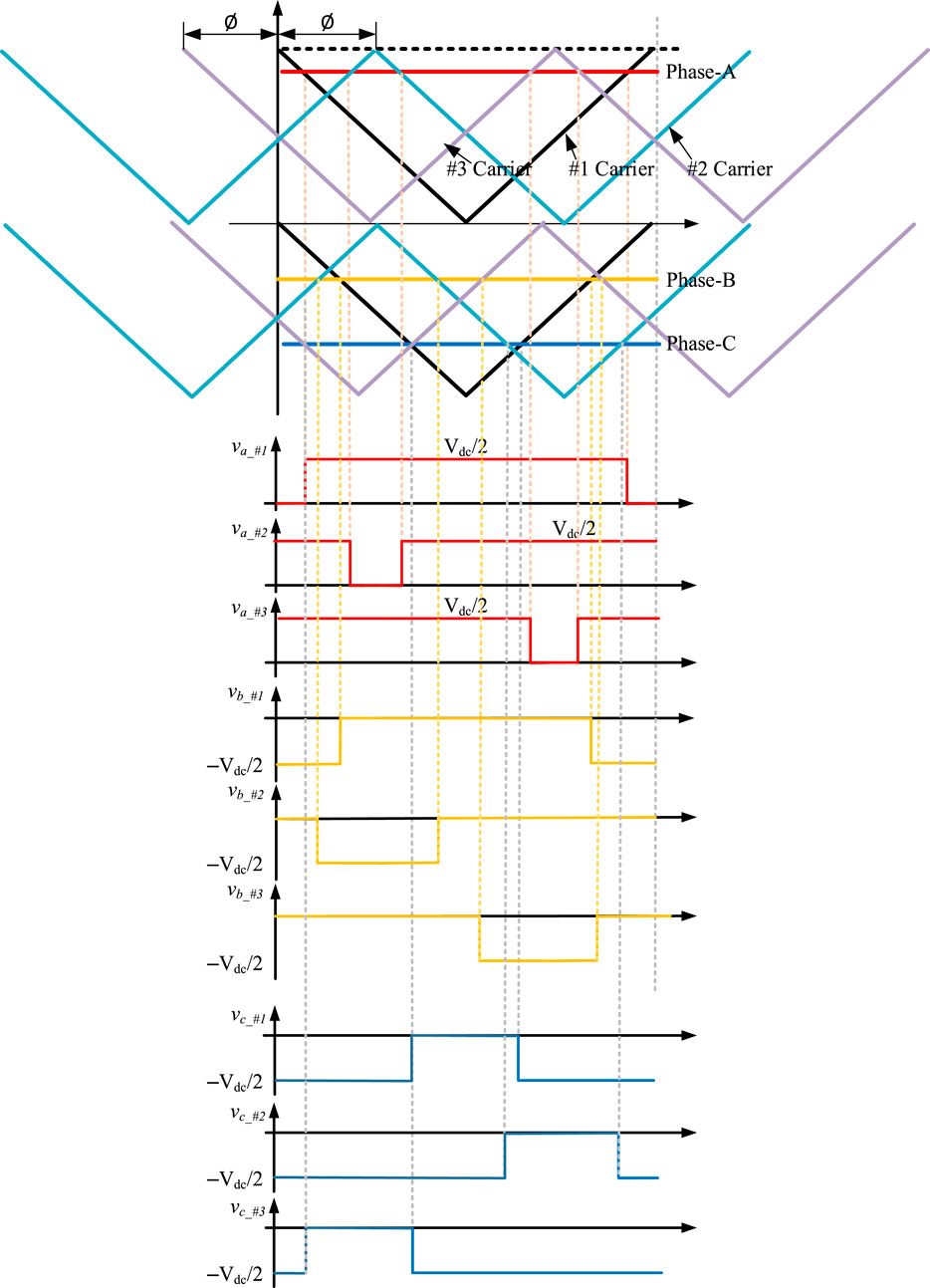
Figure 15. The intersection of the reference signals and the phase-shifted triangle wave carriers for three inverter modules.
The corresponding zero-sequence voltage component is obtained from the three-phase output voltages. Figure 16 depicts the proposed method’s zero-sequence voltage component. It can be seen that the three modules’ zero-sequence voltage has a phase shift of Ø as well. As illustrated in Figure 16, the total zero-sequence voltage of the three modules vcom_sum is with a maximum step of Vdc/3 and a variation range of–Vdc/3 to Vdc/6. For the conventional method, the maximum step is Vdc/2 and the range of change is–Vdc to Vdc/2. Therefore, compared to the traditional method, the maximum step and variation range of the zero-sequence voltage are greatly improved by the proposed triangular wave phase shifting. As a result, the proposed method can effectively improve the problem of ground current as the number of PV inverter modules increases. Therefore, the proposed method can effectively suppress the ground current to avoid exceeding the limit.
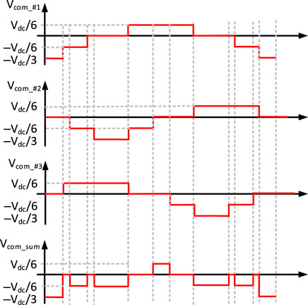
Figure 16. The zero-sequence voltage component for the carrier phase shifting method.
5.3 Software solution II: carrier frequency shifting
In this section, another method with triangulation wave carrier frequency shifting is proposed to suppress ground current. As shown in Figure 17, the triangle wave carrier frequencies for different inverter modules are shifted by Δf. Taking three of inverter modules as an example, the triangle wave carrier frequency for module #1 is f1. When compared to module #1, the triangle wave carrier frequency for module #2 is reduced by Δf, while the triangle wave carrier for module #3 is increased by Δf.
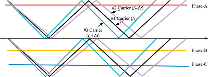
Figure 17. Carrier frequency shifting method.
Following the same method above, the reference signals and the triangle wave carriers are intersected for three inverter modules. Then, three-phase switching signals and three-phase output voltages (va, vb, vc) are obtained. With the three-phase output voltage, the corresponding zero-sequence voltage component is obtained, which is shown in Figure 18. As illustrated in Figure 18, for the zero-sequence voltage sum vcom_sum, the step is roughly Vdc/6 and the range is roughly between–Vdc/3 to Vdc/6. Therefore, compared to the traditional method, the maximum step and variation range of the zero-sequence voltage are improved with the proposed triangular wave frequency shifting. As a result, the proposed method can effectively suppress ground current as the number of PV inverter modules increases.
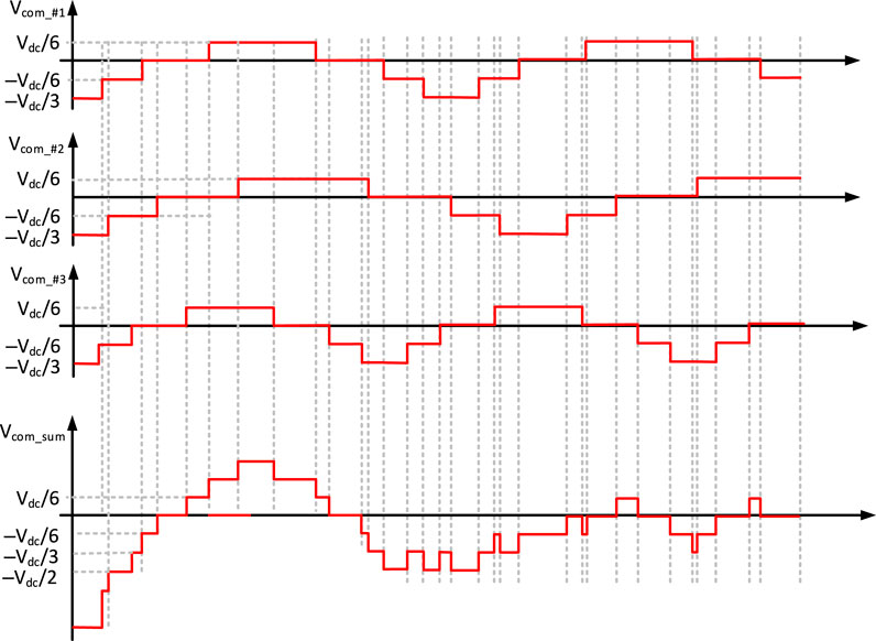
Figure 18. The zero-sequence voltage component for the carrier phase shifting method.
Figure 19 depicts an implementation method, which includes the addition of a carrier synchronization cable and a communication cable such as CAN. All PV inverter modules can realize triangulation wave carrier synchronization via the carrier synchronization cable. The carrier phase shift angles or frequencies can be transmitted via the communication cable. Normally, there is one inverter module called the master unit, which can calculate all phases or frequencies for all the inverter modules. The rest of the inverter modules are referred to slave units and they receive the phase or frequency information transmitted by the communication cable. Module #2, for example, receives the phase shift angle ΔØ2 transmitted through the communication cable and then implements carrier phase shifting.
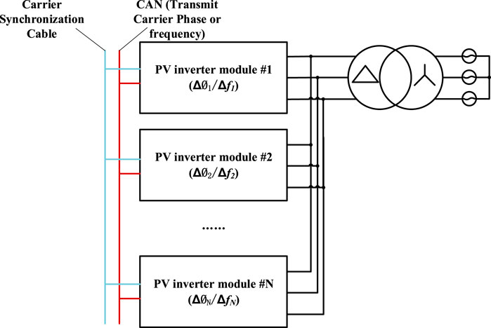
Figure 19. Carrier synchronization cable and communication cable for implementation.
From above, only the communication process for the master inverter to send phase shift angles to the slave inverters is included. This process can be completed before the inverter is started, and there are almost no additional requirements for the controller’s processing capability, making it extremely simple to deploy.
The software solution specifically proposes a method for carrier frequency shifting and phase shifting for multi-inverter systems that has shown excellent performance in inverter parallel operation and is thus appropriate for high-power applications. The greatest challenge is achieving phase angle synchronization. Nonetheless, relevant papers in detail will be published in the future.
Using TI’s TMS320F28374S as the main control chip, the phase-shifting and frequency-shifting ground current suppression method described in this paper is integrated into the existing control algorithm. TMS320F28374S’s main frequency is 200MHz, and its Read-Only Memory (ROM) resources are allocated as detailed below. The TMS320F28374S DSP chip has 64 KB flash, 1 KB One Time Programmable (OTP) ROM, and 4 KB Boot ROM. The address for Flash ranges from 0x3E8000 to 0 × 3F8000. The original code only takes about 32 KB. Because the proposed method involves phase or frequency shifting for the carriers, the extra flash space increases by only a few bytes. As a result, there is no risk of using up too much code space.
The system’s operating process is described below. There is no operating system, and a single interrupt is used. As shown in Figure 20, the entire process consists of three parts: initialization, the main loop, and the interrupt service routine (ISR). In the Initialization section, RAM is initialized using assembly with CodeStartBranch.asm. In addition, the chip peripherals, interrupts, and global variables are initialized. The main loop section implements communication with the ARM, sub-DSP, and host computer. Other tasks include digital IO processing, start-stop-restart logic, fault handling, and operating mode switching. In the ISR part, DMA triggers AD sampling at a sampling frequency of 160 kHz. The DMA interrupt is triggered every eight samples, giving the interrupt frequency of 20 kHz. The ISR performs sampling conversion and filtering, loop control, phase locking, logic processing, and a small amount of communication handling.
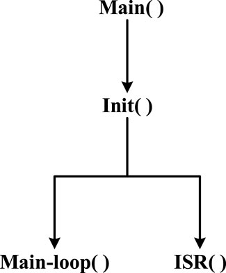
Figure 20. Software process.
In the implementation of the proposed method, only the communication process for the master inverter to send phase shift angles to the slave inverters is included. This process can be completed before the inverter is started, there will be no impact on the ISR part and the code can be implemented in the main loop. Therefore, there are almost no additional requirements for the controller’s processing capability, making it extremely simple to deploy.
6 Experimental verifications
The experiment is carried out in a PV plant with 20 inverter modules, each of which has a rated power of 25 kW. In addition, the system parameters are presented above in Table 2.
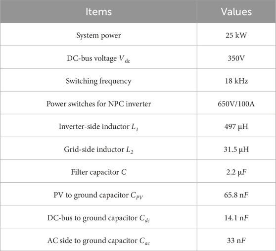
Table 2. System Parameters for the experimental setup.
Figure 21 shows the zero-sequence current i0, inductor current ia, zero-sequence current after removing high-frequency component and PV negative to ground voltage VPV_G. Although the grid current ia is of good quality, the zero-sequence current i0 contains a large number of high-frequency components and the peak-to-peak value is around 10A. Because the ground current has high-frequency components, the voltage to the ground also has high-frequency components. In Figure 21, the PV to ground voltage VPV_G has a significant high-frequency component which is around 100V, as labeled in pink color. After the high-frequency components are removed, the low-frequency variation of the zero-sequence current is large as shown by the green line. The ground-current fault is frequently triggered in this case, resulting in the system being disconnected from the grid. Therefore, as the number of PV inverter modules increases, the ground current problem worsens.
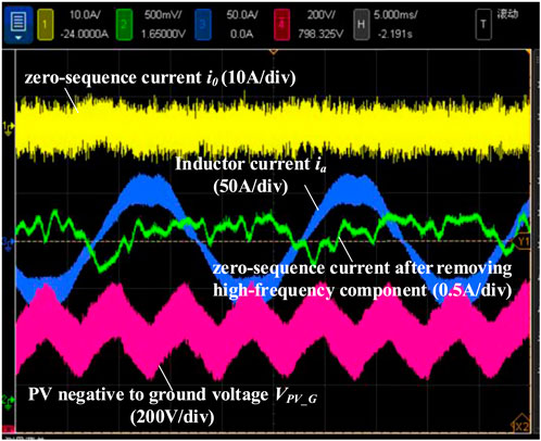
Figure 21. Zero-sequence current i0, inductor current ia, zero-sequence current after removing high-frequency component and PV negative to ground voltage.
Figure 22 depicts the zero-sequence current i0, inductor current ia, zero-sequence current after removing high-frequency component and PV negative to ground voltage VPV_G after increasing the filter capacitor C from 2.2μF to 4.4 μF. Because the high-frequency components are reduced, the quality of the grid current ia improves. Furthermore, the high-frequency components of the zero-sequence current i0 are greatly reduced and the peak-to-peak value is around 0.5A. Because the high-frequency components of the ground current are reduced, the high-frequency components of the ground voltage are suppressed as well. The high-frequency components of PV to ground voltage VPV_G, for example, are significantly reduced which is around 10V. The low-frequency variation of the zero-sequence current is reduced as well, as shown by the green line. Therefore, the method of increasing the capacitance of filter capacitors connected to the DC-bus is effective. The ground-current fault can be avoided, and the ground current problem can be solved.
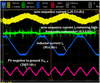
Figure 22. After increasing the filter capacitor from 2.2 μF to 4.4μF, zero-sequence current i0, inductor current ia, zero-sequence current after removing high-frequency component and PV negative to ground voltage with hardware solution.
Figure 23 shows the zero-sequence current i0, inductor current ia, zero-sequence current after removing high-frequency component and PV negative to ground voltage VPV_G when the carrier frequency shifting software solution is applied. The carrier frequencies are shifted by 1 kHz with respect to each other for every four inverter modules, making them 16 kHz, 17 kHz, 18 kHz, and 19 kHz, respectively. When compared to the original method in Figure 21, the quality of the grid current ia improves and the high-frequency components are reduced. The high-frequency components of the zero-sequence current i0 are also reduced and the peak-to-peak value is around 7A. The high-frequency components of the ground voltage are also suppressed. In Figure 23, the high-frequency components of PV to ground voltage VPV_G are reduced which is around 60V. As shown by the green line, the low-frequency variation of the zero-sequence current is also reduced. Therefore, the carrier frequency shifting method is effective to some extent. The ground-current faults can be reduced, and the ground current problem can be alleviated.
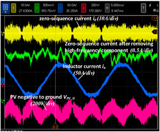
Figure 23. Zero-sequence current i0, inductor current ia, zero-sequence current after removing high-frequency component and PV negative to ground voltage when the software solution of carrier frequency shifting is applied.
In response to grid voltage fluctuations, the inverter uses dynamic reactive power regulation technology to quickly and precisely control reactive power. By adjusting the inductive or capacitive reactive power output, it actively supports or mitigates grid voltage fluctuations.
As shown in Figure 24a, when the grid is normal, the Root Mean Square (RMS) value of the grid voltage is 230V. At t1, the grid voltage is increased to 260V, and the inverter implements high-voltage ride through and outputs reactive power. At t2, the grid voltage returns to normal, and the inverter’s high voltage ride through is completed. As shown in Figure 24b, at t1, the grid voltage is decreased to 191V, and the inverter implements low-voltage ride through and outputs reactive power. At t2, the grid voltage returns to normal, and the inverter’s low voltage ride through is completed.In the event of a voltage imbalance, the positive and negative sequence separation method is used to divide the three-phase unbalanced voltage into positive and negative sequence voltages. By suppressing the negative sequence voltage, normal output is achieved. As shown in Figure 25b, the grid voltage is unbalanced, where the grid voltages of three phases are 279.3V, 230V and 179.5V. With the positive and negative sequence separation method applied, the output power can be maintained as steady.
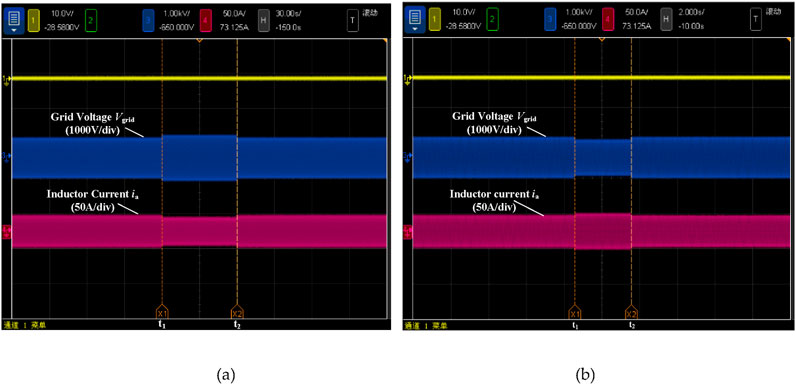
Figure 24. Grid voltage high voltage or low voltage ride through, (a) high voltage ride through, (b) low voltage ride through Regarding grid frequency fluctuations, the inverter employs rapid frequency support technology to quickly adjust active power, thereby suppressing frequency fluctuations and maintaining grid frequency stability. As illustrated in Figure 25a, when the grid frequency is higher than normal, the inverter limits the output power and reduces the active power injected into the grid. Similarly, when the grid frequency is lower than normal, the inverter increases the output power, which supports the grid by injecting additional active power.
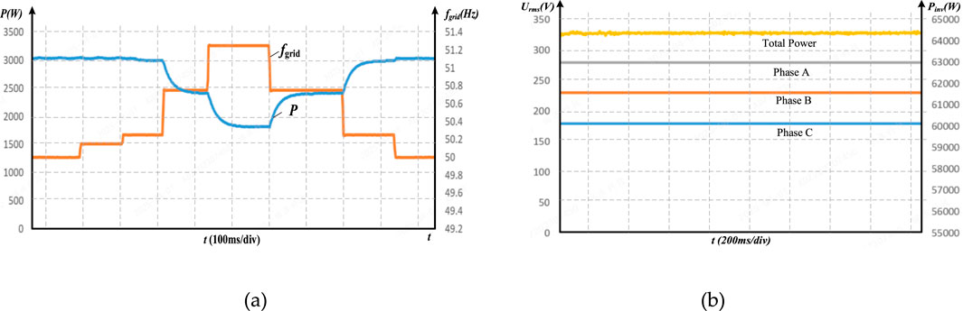
Figure 25. Grid frequency fluctuation and voltage imbalance, (a) grid frequency fluctuations, (b) grid voltage imbalance.
Therefore, the ground current suppression method described in this paper is unaffected by grid fluctuations or unbalanced loads. Furthermore, it does not worsen grid fluctuations or inverter output imbalances. As a result, this aspect of knowledge is not discussed further in this paper.
7 Cost assessment
The ground current suppression scheme discussed in this article has nothing to do with PV modules, so there is no need for them to be replaced and, as a result, the associated costs are avoided.
The phase-shifting and frequency-shifting methods described in this paper have minimal impact on the main controller’s storage space and processing time. Therefore, there is no need to upgrade the main control chip or add an external memory chip. It is only necessary to upgrade the code to effectively suppress the problem of excessive ground current. As a result, the controllers will not incur any additional costs.
For multi-inverter communication, it can be accomplished using previously established communication lines, such as 485 communication lines, eliminating the need for additional costs.
The hardware solution’s main cost is for additional filter capacitors. However, it is significantly less expensive than adding switch transistors in other alternatives. This paper’s proposal to add capacitors between the inverter output neutral point and the dc-bus midpoint will result in a slight cost increase. A filter capacitor (2.2 μF/450V) costs about ¥0.2. Adding six filter capacitors to a 350 kW PV inverter costs only ¥1.2. Compared to the total cost of ¥30,000, the additional costs are minimal. Traditional methods of adding switching devices and diodes to a dc/ac circuit typically cost more than ¥60. As a result, the economics of the proposed scheme are favorable.
8 Conclusion
In large PV plants, a large number of PV inverters are linked together at the grid-side to generate more power. However, this worsens the ground current problem, which can result in a ground current fault, and cause the inverter system failed and disconnected from the grid. In this paper, the solutions, including hardware and software, are proposed to suppress the ground current. The hardware solution is to increase the capacitance of filter capacitors connected to the DC-bus, directing more ground current to the inverter rather than the grid to reduce the ground current. Additionally, the software solutions, including carrier phase shifting and carrier frequency shifting, are proposed to suppress ground current. In the software solutions, the ground current for the PV inverters can be cancelled each other, which can alleviate the ground current problem.
First, the system architecture is presented. The concept of connecting the neutral point of the filter capacitors to the DC-bus midpoint is explained. The zero-sequence mathematical model is then built.
The effect of the zero-sequence voltages of the DC/AC converter and the grid on the zero-sequence current is investigated. According to the analysis, when the zero-sequence current is primarily caused by the zero-sequence voltage of the DC/AC converter, increasing the value of the capacitors connected to the DC-bus can greatly improve the effect of the zero-sequence current suppression.
The control architecture is presented. The method to obtain the three-phase output voltage and zero-sequence components for PV inverters is explained. From the analysis, as the number of PV inverter modules increases, the ground current worsens.
Two software solutions, carrier phase shifting and carrier frequency shifting, are proposed to suppress ground current, particularly in systems with a large number of PV inverter modules. The concept and implementation for two proposed software solutions are detailed. From the analysis, the proposed two methods improve the maximum step and variation range of the zero-sequence voltage over the traditional method.
Finally, the experiment is conducted in a PV plant equipped with 20 inverter modules. According to the results of the experiments, the hardware and software methods are both effective. The ground-current fault and the ground current problem can both be avoided with the proposed method.
In the future, as renewable energy becomes more popular, more and more grid-connected inverters will be applied. This proposed method can fundamentally solve the ground current problem, especially in large PV plants equipped a large number of PV inverter modules. The most difficult aspect of the hardware solution is dealing with various scenarios in which leakage current is caused by either the inverter or the grid. As a result, the additional filter capacitors could be installed on either the inverter or grid side. Future work will focus on more practical aspects of this issue. The software solution proposes a method for carrier phase shifting in a multi-inverter system. The most difficult challenge is achieving phase angle synchronization. We did not go into great detail about this topic because of the limited space in this article. Nonetheless, relevant papers will appear in the future.
Data availability statement
The original contributions presented in the study are included in the article/supplementary material, further inquiries can be directed to the corresponding author.
Author contributions
WZ: Methodology, Writing – original draft. DL: Supervision, Writing – review and editing. YW: Conceptualization, Writing – original draft. PX: Software, Writing – review and editing. BL: Validation, Writing – original draft.
Funding
The author(s) declare that financial support was received for the research and/or publication of this article. This work was funded by National Key R&D Program of China (2024YFB3814000).
Conflict of interest
Authors WZ, YW, PX, and BL were employed by Ginlong Technologies Co., Ltd.
The remaining authors declare that the research was conducted in the absence of any commercial or financial relationships that could be construed as a potential conflict of interest.
Generative AI statement
The author(s) declare that no Generative AI was used in the creation of this manuscript.
Publisher’s note
All claims expressed in this article are solely those of the authors and do not necessarily represent those of their affiliated organizations, or those of the publisher, the editors and the reviewers. Any product that may be evaluated in this article, or claim that may be made by its manufacturer, is not guaranteed or endorsed by the publisher.
References
Anand, V., Singh, V., Sathik, J., and Almakhles, D. (2023). Single-stage five-level common ground transformerless inverter with extendable structure for centralized photovoltaics. CSEE J. Power Energy Syst. 9 (1), 37–49. doi:10.17775/CSEEJPES.2022.02700
Azizi, A., Akhbari, M., Danyali, S., Tohidinejad, Z., and Shirkhani, M. (2025). A review on topology and control strategies of high-power inverters in large-scale photovoltaic power plants. Heliyon 11 (3), e42334. 2405-8440. doi:10.1016/j.heliyon.2025.e42334
Barzegarkhoo, R., Farhangi, M., Lee, S. S., Aguilera, R. P., Blaabjerg, F., and Siwakoti, Y. P. (2023). A novel active neutral point-clamped five-level inverter with single-stage-integrated dynamic voltage boosting feature. IEEE Trans. Power Electron. 38 (6), 7796–7809. doi:10.1109/TPEL.2023.3257959
Concari, L., Barater, D., Concari, C., Toscani, A., Buticchi, G., and Liserre, M. (2017). “H8 architecture for reduced common-mode voltage three-phase PV converters with silicon and SiC power switches,” in Iecon 2017 - 43rd annual conference of the (Beijing, China: IEEE Industrial Electronics Society), 4227–4232. doi:10.1109/IECON.2017.8216725
Gonzalez, R., Lopez, J., Sanchis, P., and Marroyo, L. (2007). Transformerless inverter for single-phase photovoltaic systems. IEEE Trans. Power Electron. 22 (2), 693–697. doi:10.1109/TPEL.2007.892120
Gyawali, B., Rukhsar, , Ajmal, A. M., and Yang, Y. (2024). Design and analysis of a triple-input three-level PV inverter with minimized number of MPPT controllers. Energies 17, 5380. doi:10.3390/en17215380
Holmes, D. G., and Lipo, T. A. (2003). Pulse width modulation for power converters: principles and practice. John Wiley and Sons.
Ji, B., Wang, J., and Zhao, J. (2013). High-efficiency single-phase transformerless PV H6 inverter with hybrid modulation method. IEEE Trans. Industrial Electron. 60 (5), 2104–2115. doi:10.1109/TIE.2012.2225391
Khan, M. N. H., Forouzesh, M., Siwakoti, Y. P., Li, L., Kerekes, T., and Blaabjerg, F. (2020). Transformerless inverter topologies for single-phase photovoltaic systems: a comparative review. IEEE J. Emerg. Sel. Top. Power Electron. 8 (1), 805–835. doi:10.1109/JESTPE.2019.2908672
Liu, B., Su, M., Yang, J., Song, D., He, D., and Song, S. (2017). Combined reactive power injection modulation and grid current distortion improvement approach for H6 transformer-less photovoltaic inverter. IEEE Trans. Energy Convers. 32 (4), 1456–1467. doi:10.1109/TEC.2017.2712741
Mohon, N., Undeland, T. M., and Robbins, W. P. (1995). Power electronics converters, applications and design. 2nd ed. New York: Wiley.
Nabae, A., Takahashi, I., and Akagi, H. (1981). A new neutral-point-clamped PWM inverter. IEEE Trans. Ind. Appl. (5), 518–523. doi:10.1109/tia.1981.4503992
Noroozi, N., Zolghadri, M. R., and Yaghoubi, M. (2017). “A novel modulation method for reducing common mode voltage in three-phase inverters,” in 2017 IEEE international conference on environment and electrical engineering and 2017 IEEE industrial and commercial power systems europe (EEEIC/I&CPS europe) (Milan, Italy), 1–5. doi:10.1109/EEEIC.2017.7977818
Ranjan Satpathy, P., Aljafari, B., Babu Thanikanti, S., Nwulu, N., and Sharma, R. (2024a). A multi-string differential power processing based voltage equalizer for partial shading detection and mitigation in PV arrays. Alexandria Eng. J. 104, 12–30. ISSN 1110-0168. doi:10.1016/j.aej.2024.05.105
Ranjan Satpathy, P., Ramachandaramurthy, V. K., Radha Krishnan, T. R., Pulenthirarasa, S., and Padmanaban, S. (2024b). Power and efficiency enhancement of solar photovoltaic power plants through grouped string voltage balancing approach. Energy Convers. Manag. X 24, 100711. 2590-1745. doi:10.1016/j.ecmx.2024.100711
Sharma, S., Jately, V., Kuchhal, P., Kala, P., and Azzopardi, B. (2023). A comprehensive review of flexible power-point-tracking algorithms for grid-connected photovoltaic systems. Energies 16 (15), 5679. doi:10.3390/en16155679
Tofigh Azary, M., Sabahi, M., Babaei, E., and Abbasi Aghdam Meinagh, F. (2018). Modified single-phase single-stage grid-tied flying inductor inverter with MPPT and suppressed leakage current. IEEE Trans. Industrial Electron. 65 (1), 221–231. doi:10.1109/TIE.2017.2719610
Xiao, H., Liu, X., and Lan, K. (2014). Optimised full-bridge transformerless photovoltaic grid-connected inverter with low conduction loss and low leakage current. IET Power Electron. 7, 1008–1015. doi:10.1049/iet-pel.2013.0404
Xiao, H., Xie, S., Chen, Y., and Huang, R. (2011). An optimized transformerless photovoltaic grid-connected inverter. IEEE Trans. Industrial Electron. 58 (5), 1887–1895. doi:10.1109/TIE.2010.2054056
Xu, T., Lei, M., Liu, W., Meng, F., Lv, D., Hu, W., et al. (2023). Energy balance in a standalone PV battery hybrid generation system on solar-powered aircraft using the model predictive control method. Energies 16 (17), 6185. doi:10.3390/en16176185
Zhang, W., He, Y., Wang, X., and Chen, J. (2023c). A comprehensive method for online switch fault diagnosis and capacitor condition monitoring of three-level T-type inverters. IEEE Trans. Power Electron. 38 (8), 10183–10195. doi:10.1109/TPEL.2023.3262758
Zhang, W., Wang, Y., Xu, P., Li, D., and Liu, B. (2023a). Evaluation and improvement of backup capacity for household electric vehicle uninterruptible power supply (EV-UPS) systems. Energies 16, 4567. doi:10.3390/en16124567
Zhang, W., Wang, Y., Xu, P., Li, D., and Liu, B. (2023b). A current control method for grid-connected inverters. Energies 16, 6558. doi:10.3390/en16186558
Keywords: PV inverters, ground current suppression, zero-sequence, carrier phase shifting, grid-connected
Citation: Zhang W, Li D, Wang Y, Xu P and Liu B (2025) A ground current suppression method for systems with a large number of photovoltaic (PV) inverters. Front. Energy Res. 13:1582264. doi: 10.3389/fenrg.2025.1582264
Received: 24 February 2025; Accepted: 18 April 2025;
Published: 29 April 2025.
Edited by:
Marif Daula Siddique, Swinburne University of Technology, AustraliaReviewed by:
Priya Ranjan Satpathy, Universiti Tenaga Nasional, MalaysiaAndrea Toscani, University of Parma, Italy
Copyright © 2025 Zhang, Li, Wang, Xu and Liu. This is an open-access article distributed under the terms of the Creative Commons Attribution License (CC BY). The use, distribution or reproduction in other forums is permitted, provided the original author(s) and the copyright owner(s) are credited and that the original publication in this journal is cited, in accordance with accepted academic practice. No use, distribution or reproduction is permitted which does not comply with these terms.
*Correspondence: Wenping Zhang, d2VucGluZy56aGFuZ0BnaW5sb25nLmNvbQ==