 Siqi Huang
 Lu Fan1,2
- 1Department of Electrical Engineering, Shanghai Jiao Tong University, Shanghai, China
- 2State Key Laboratory of High-Efficiency Special Cable Technology, Shanghai, China
- 3State Grid Shanghai Municipal Electrical Power Company, Shanghai, China
Switching-induced stress waves (SSW) are recognized as a promising non-invasive technology for real-time monitoring of power module packaging failures, though limited by the lack of a comprehensive understanding of their characteristics and propagation mechanisms. In this study, a dedicated SSW detection platform was developed for SiC MOSFET power modules, where the mechanical wave nature was verified through time-delay analysis. Dominant frequency components at 150 kHz and 270 kHz were identified using both piezoelectric ceramic and PVDF sensors. Experimental investigations further demonstrated that the time-domain parameters of SSW were predominantly influenced by bus voltage (UDC), followed by load current (IR), whereas principal frequency components remained stable across operational conditions. Propagation effects through the module were systematically analyzed via finite element modeling, revealing a 5.82% increase in signal amplitude and 5.88% spectral bandwidth expansion after transmission. These results confirm that sensor-captured signals can be effectively equated to original chip vibrations in defect-free propagation paths.
1 Introduction
Power electronics technology has witnessed remarkable advancements over the past three decades, extending its applications from conventional power systems, transportation, and communication networks to emerging sectors like renewable energy generation and intelligent home appliances (Zare et al., 2019; Wang et al., 2021). The emergence of wide-bandgap semiconductor devices, particularly silicon carbide (SiC) and gallium nitride (GaN), has further accelerated this evolution. Leveraging their exceptional breakdown voltage, high-frequency switching capabilities, and thermal resilience (Kimoto, 2015; Wen et al., 2021), these materials have become driving forces behind the development of power electronics toward higher voltage ratings, increased power capacity, and improved power density (Wang, 2014; Ding et al., 2022).
Nevertheless, the deployment of wide-bandgap devices introduces critical technical challenges. Significant thermal stresses generated by elevated junction temperatures during operation exacerbate packaging degradation mechanisms such as bond wire detachment, solder layer creep failure, and ceramic substrate cracking (Li et al., 2022). Industry statistics indicate that approximately 55% of power module failures stem from such thermo-mechanical failures (Falck et al., 2018), highlighting the growing imperative for reliability research in this domain.
Current health monitoring methodologies for power devices predominantly exploit three categories of physical parameters, each presenting distinct limitations. Electrical parameters, while readily accessible, suffer from susceptibility to operational circuit conditions, restricting their adaptability in practical applications (Ren et al., 2015). Magnetic parameter detection necessitates the integration of miniature sensors, thereby imposing structural modifications on standardized module architectures (Brauhn et al., 2017). Thermal monitoring techniques typically rely on external infrared imaging equipment, which inherently compromises real-time responsiveness (Li et al., 2016). These inherent restrictions contribute to persistent engineering challenges, including undetected incipient faults and escalating operational maintenance costs. Consequently, the development of non-invasive, high-sensitivity online detecting strategies remains a critical frontier in power electronics research.
Stress wave detection technology, as a non-destructive testing method, has gained widespread application across multiple domains including wind turbine blade damage monitoring (Chen et al., 2013), partial discharge detection (Zhou et al., 2019; Maki et al., 2017), and pipeline leak identification (Jiang et al., 2002), owing to its advantages of rapid response, real-time capability, and non-invasive nature. The application of this technology in power semiconductors has evolved along two parallel paths. For silicon IGBTs, the foundational work by Kärkkäinen et al. (2014) first identified acoustic emission (stress waves) signatures during normal switching operations, with subsequent aging studies (Müller et al., 2016; Davari et al., 2018) preliminarily validating the feasibility of stress wave-based condition monitoring. Research (Li et al., 2020) identified distinct high-frequency and low-frequency components in IGBT stress waves, revealing a clear linear relationship between low-frequency components and turn-off current. Recent advancements by Chen’s group (Zhou et al., 2022; Geng et al., 2022; Geng et al., 2023) have significantly deepened the mechanistic understanding: Zhou et al. (2022) established transient Lorentz forces as the primary excitation source through coupled electromagnetic-structural analysis, Geng et al. (2022) developed differential sensor configurations to suppress electromagnetic interference, and Geng et al. (2023) proposed a comprehensive analytical model linking turn-off di/dt to stress wave generation efficiency. In contrast, research on silicon MOSFETs has taken a different approach. Works by He et al. (2021) revealed dual-component stress wave generation mechanisms, attributing high-frequency signals to drain-source voltage oscillations while connecting low-frequency components with gate charge dynamics. This was further expanded by Bai et al. (2021) who systematically investigated the effects of measurement surfaces, electrical parameters, and filtering on Si MOSFET stress waves.
Despite these advancements, critical research gaps persist. First, while SiC MOSFETs are increasingly adopted in high-frequency and high-speed applications due to their superior material properties, investigations on their stress wave characteristics remain disproportionately scarce compared to silicon-based devices. Second, existing studies predominantly focus on generation mechanisms and external signal characterization, with limited attention to stress wave propagation dynamics within power device packaging structures. This critical oversight leaves the influence mechanisms of packaging failures on stress wave signatures fundamentally unresolved.
This study systematically investigates the switching-induced stress wave characteristics of SiC MOSFET power modules through an integrated experimental and simulation approach. A resistive-load-based pulsed test platform was first established, where time-delay analysis and comparative measurements using piezoelectric ceramic and PVDF sensors confirmed the mechanical wave nature and dominant frequency characteristics of the observed stress waves. Multi-operational-condition experiments were subsequently conducted to analyze the time-domain effects of bus voltage and load current variations on stress wave attributes, with results demonstrating the operational robustness of principal spectral components. Finally, a structural mechanics model was developed using finite element software, enabling correlation analysis between the stress wave generation sources and experimentally measured signal features.
2 Methodology and experimental analysis of switching-induced mechanical stress waves
2.1 Methodology and experimental platform design
Switching-induced stress waves are unique mechanical signals generated by electrical transients during the switching processes of power devices. These processes are typically controlled using pulsed test circuits. Figure 1 illustrates the schematic of a single-pulse test circuit based on a resistive load. The operational states of the power device under single-pulse testing are described as follows:
• Prior to time t1: Both VT1 and VT2 remain in the off-state, with the voltage across VT2 (UVT2) equaling UDC.
• At time t1: VT2 is turned on, causing its terminal voltage to abruptly drop to zero, while the current through VT2 equals the resistive current IR.
• At time t2: VT2 is turned off, restoring the voltage across it to UDC and reducing the current to zero.
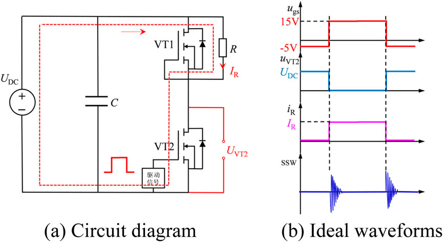
Figure 1. Schematic of the pulsed test circuit. (a) Circuit diagram. (b) Ideal waveforms.
During the transient intervals of VT2 turn-on and turn-off, stress wave signals can be detected using stress wave sensors.
As illustrated in Figure 2, the methodology for studying stress waves in power devices comprises three sequential phases:
• Stress Wave Generation Circuit: The device under test (DUT) is integrated into a pulsed test circuit. A single-pulse signal is applied to the gate terminal to control the turn-on and turn-off operations of the DUT. During these switching instants, electrical transients excite stress waves within the device.
• Stress Wave Reception and Extraction: A stress wave sensor, coupled to the DUT surface along the wave propagation path via an acoustic coupling agent, detects and captures the stress waves. The raw signals are preprocessed using application-specific filters and amplifiers to optimize signal-to-noise ratio. The conditioned signals are then recorded using a digital oscilloscope.
• Post-Processing: The acquired stress wave signals are processed in MATLAB to extract time-domain characteristics (e.g., amplitude, propagation time), frequency-domain features (e.g., spectral components via FFT), and other relevant parameters. The results are systematically analyzed to characterize the properties of switching-induced stress waves.
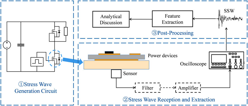
Figure 2. Research methodology for switching-induced stress waves in power devices.
The stress wave testing platform integrates two functional subsystems: a stress wave generation circuit and a signal reception system, with the physical setup depicted in Figure 3. The generation circuit employs a pulsed test circuit board to drive the device under test (DUT), specifically a SiC MOSFET power module (model: GCMX020A120B2B1P-3393646), under controlled switching conditions. A high-voltage DC power supply provides the main bias, while a signal generator delivers single-pulse gate signals to initiate turn-on/off transients. Critical electrical parameters, including drain-source voltage and load current, are monitored using a differential probe and a current sensor, respectively.
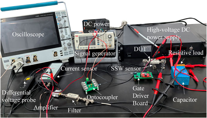
Figure 3. Photograph of the experimental platform.
For stress wave detection, a PXR15 piezoelectric ceramic sensor (>67 dB sensitivity, 100kHz–400 kHz bandwidth with 150 kHz resonance frequency) is acoustically coupled to the DUT surface using silicone grease. The sensor is positioned on the module underside with 1.7 mm separation from the chip through the direct-bonded copper (DBC) substrate. The raw sensor output undergoes preconditioning via a low-pass filter (400 kHz cutoff) and a low-noise amplifier (50 dB gain) to enhance signal fidelity before digitization by a high-speed oscilloscope. This integrated architecture enables synchronized acquisition of electrical switching events and their corresponding mechanical wave signatures.
2.2 Validation of stress wave components via time-delay comparison
The transient signals generated during the switching instants of SiC MOSFET power modules comprise distinct high-frequency and low-frequency components. High-frequency components (ranging from several MHz to tens of MHz) propagate predominantly as electromagnetic waves, exhibiting rapid propagation velocities and short durations (approximately hundreds of nanoseconds). In contrast, low-frequency components (spanning tens of kHz to several hundred kHz) correspond to mechanical stress waves, characterized by slower propagation speeds and extended durations (typically hundreds of microseconds).
Despite the incorporation of a low-pass filter with a 400 kHz cutoff frequency in the experimental setup, residual interference from high-frequency components persists in the detected signals. This phenomenon arises due to non-ideal filter attenuation characteristics and electromagnetic coupling effects between power interconnects and sensor pathways, which allow partial high-frequency energy to bypass the filtering stage.
Electromagnetic waves propagate through metallic media at velocities approaching the speed of light (c ≈ 3 × 10⁸ m/s), whereas mechanical waves in aluminum exhibit substantially slower propagation characteristics. The maximum theoretical velocity for mechanical waves in such media corresponds to the longitudinal wave speed (vlong ≈ 6.4 × 10³ m/s), with guided wave velocities - dependent on geometric constraints and mode shapes - always remaining below this threshold. To unambiguously verify the existence of switching-induced mechanical stress waves, an experimental methodology exploiting this fundamental speed disparity is implemented.
The signal propagation path between the power module and the sensor is intentionally routed through an elongated aluminum plate. By incrementally relocating the sensor along the plate’s longitudinal axis (pos.1 and pos.2 in Figure 4), the time delay (Δt) between the switching transient and the detected signal is systematically measured. A positive correlation between Δt and the sensor’s displacement distance (Δd) would indicate mechanical wave propagation, as the delay would adhere to the relationship Δt ≈ Δd/vguided, where vguided represents the guided wave velocity (necessarily vguided ≤ vlong). Conversely, negligible time delay variations would suggest electromagnetic interference, given the near-instantaneous propagation of EM waves through the metallic structure.
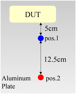
Figure 4. Schematic of sensor positions on the aluminum plate.
The experimental results are presented in Figure 5, where two spike signals are observed at the turn-on and turn-off instants. Pos. 1 displays the raw detection signal when the sensor is at Position 1, revealing aliasing between high-frequency residual interference and low-frequency stress waves during the turn-on phase, which obscures the identification of the stress wave initiation point. Pos. 2 corresponds to the sensor relocated to Position 2, where temporal separation between high-frequency interference and stress wave signals is achieved due to mechanical wave propagation delays. However, the prolonged duration of low-frequency mechanical waves (hundreds of microseconds) exceeds the switching period under the tested conditions, resulting in temporal overlap between the turn-on stress wave and turn-off signal. This study resolves stress wave identification by analyzing the time-delay characteristics in the turn-on phase.
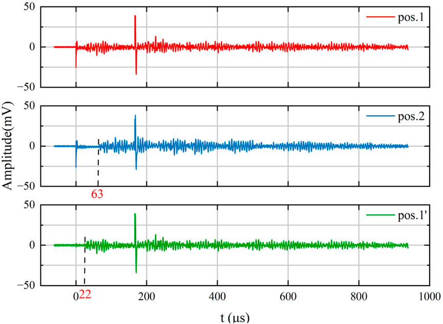
Figure 5. Signal time-delay comparison across sensor positions.
Applying matched filtering to pos. 1 based on the temporal separation features established from pos. 2, a decoupled signal (pos. 1′) is obtained. The processed results reveal a stress wave initiation time of 22 μs at position 1 and 63 μs at position 2, yielding a measured time delay of Δt = 41 μs. The guided wave velocity is calculated as vguided = 3,049 m/s, which is orders of magnitude lower than the speed of electromagnetic waves (c ≈ 3 × 10⁸ m/s), thereby confirming the mechanical nature of the detected signals. Furthermore, the derived vguided aligns with the theoretical velocity range for guided waves propagating in the 6 mm-thick aluminum plate, validating the experimental methodology and wave mode analysis.
2.3 Stress wave spectral analysis
Fast Fourier Transform (FFT) analysis is applied to the extracted turn-on and turn-off stress wave signals from the power module. As shown in Figures 6a,b, the spectral distributions of turn-on and turn-off signals exhibit similar characteristics, with primary peaks centered at 157 kHz and secondary peaks near 270 kHz.
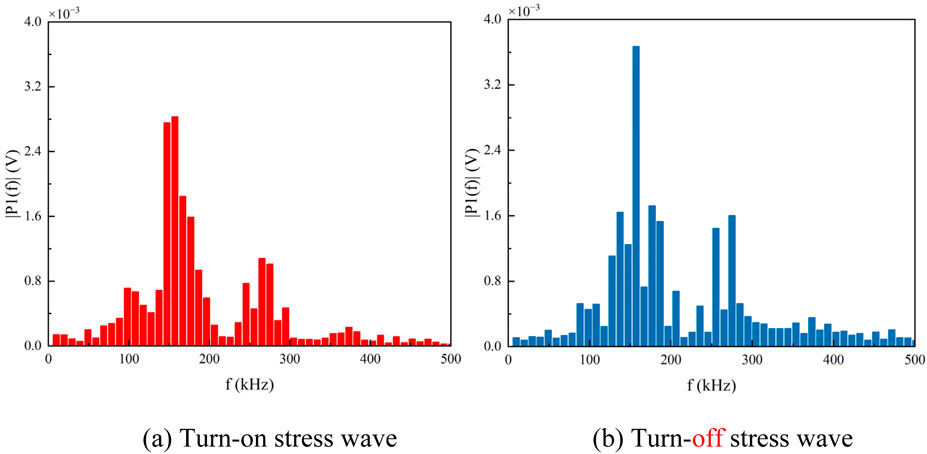
Figure 6. Spectrum of stress wave signals. (a) Turn-on stress wave. (b) Turn-off stress wave.
Amplitude analysis reveals that the turn-off stress wave’s primary peak magnitude (×3.610−3) significantly exceeds that of the turn-on stress wave (2.8 × 10⁻³). The turn-off spectrum also demonstrates broader energy distribution, maintaining notable energy levels within the 300–450 kHz range, whereas the turn-on stress wave shows rapid attenuation in this frequency band. This disparity may arise from the prolonged duration of turn-on events and potential contamination of the turn-off signal by residual turn-on components.
To circumvent the frequency response limitations of conventional piezoelectric ceramic sensors (typical bandwidth <1 MHz), this study employs a custom-made polyvinylidene fluoride (PVDF) piezoelectric film sensor fabricated with 110 μm silver-coated piezoelectric film. The PVDF sensor, coupled using silicone grease and positioned identically to the ceramic sensor, is paired with a 100 kHz high-pass filter to capture potential high-frequency mechanical wave components (MHz-range). PVDF sensors exhibit broad frequency response characteristics, achieving up to 1 GHz at room temperature, with piezoelectric effects spanning quasi-static, low-frequency, high-frequency, ultrasonic, and ultra-high-frequency regimes (Dang, 2019). This capability enables simultaneous monitoring of low-frequency mechanical waves and high-frequency vibration modalities.
The PVDF sensor was positioned at the previously defined Sensor Position 2 (Pos. 2). The acquired signal, shown in Figure 7a, demonstrates that the PVDF’s wide bandwidth captures additional high-frequency interference introduced by switching transients, which superimposes on the stress wave signals.
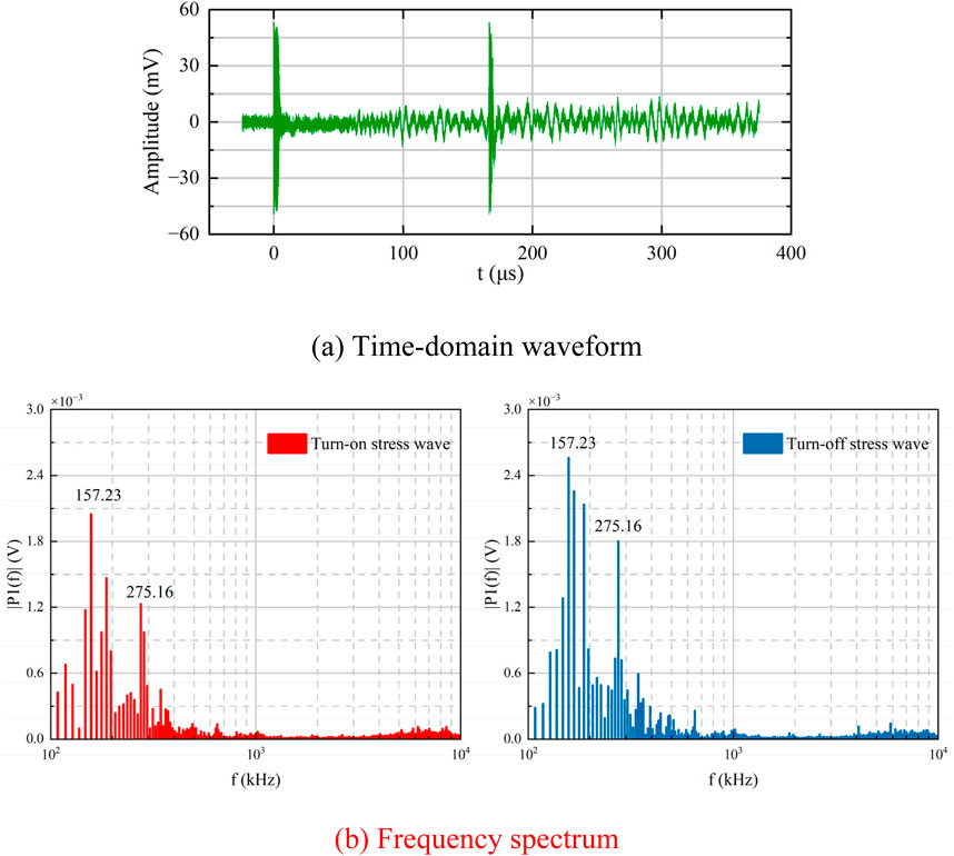
Figure 7. Signals detected by the PVDF sensor. (a) Time-domain waveform. (b) Frequency spectrum.
The extracted stress wave signals undergo spectral analysis (Figure 7b), revealing nearly identical frequency distributions between turn-on and turn-off events. Both spectra exhibit dominant peaks at 157 kHz and 275 kHz, with no significant high-frequency components. These spectral characteristics align with measurements obtained from the piezoelectric ceramic sensor, confirming that the switching-induced stress waves in this SiC MOSFET module predominantly reside around 150 kHz and 270 kHz.
3 Characteristics of switching-induced stress waves under varying operating conditions
3.1 Time-domain characteristics
This study employs a single-pulse test platform to detect switching-induced stress wave signals under various bus voltages (UDC) and load currents (IR), all within the device’s safe operating area. Figure 8 illustrates the time-domain response characteristics of stress waves across these operating conditions.
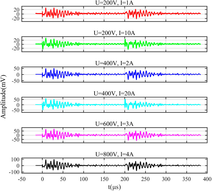
Figure 8. Stress waves under varying operating conditions.
Feature parameters such as the amplitudes and peak-to-peak values of both turn-on and turn-off stress waves were extracted from the time-domain signals illustrated in Figure 8. The data presented in Table 1 reveal significant variations in these parameters across different voltage and current operating conditions. A consistent upward trend is observed for both amplitude and peak-to-peak values of the stress waves as voltage and current increase. For example, under U = 200 V and I = 1 A, the turn-on stress wave exhibits an amplitude of 28.88 mV and a peak-to-peak value of 48.77 mV, while increasing the voltage to 800 V and current to 4 A elevates these values to 101.38 mV and 176.06 mV, respectively. Similarly, the turn-off stress wave under U = 200 V and I = 1 A shows an amplitude of 23.10 mV and a peak-to-peak value of 45.31 mV, which rise to 84.93 mV and 154.50 mV at U = 800 V and I = 4 A.
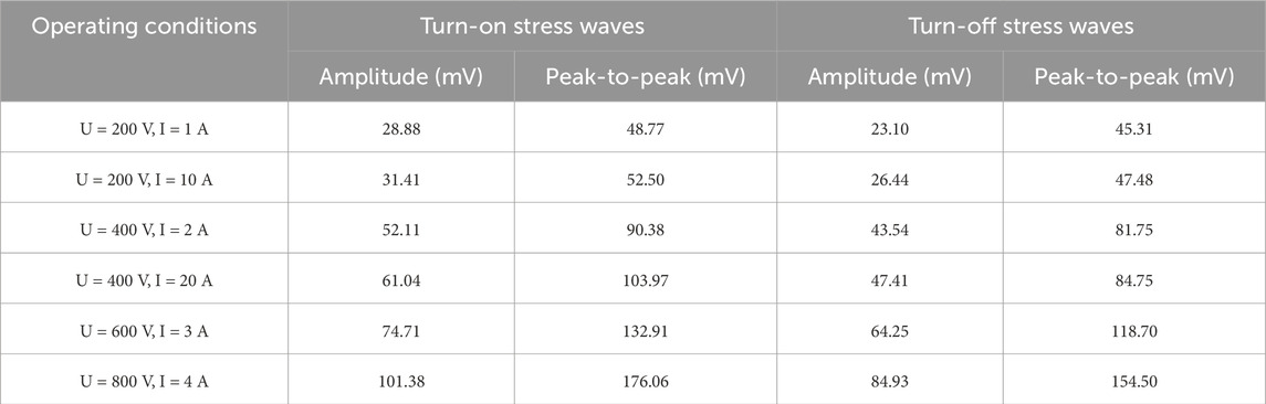
Table 1. Time-domain parameters of switching-induced stress waves under varying operating conditions.
The increase in both voltage and current enhances stress wave intensity, yet voltage variations contribute significantly more to parameter increments compared to current. Under constant voltage, even a tenfold increase in current yields minimal growth in amplitude and peak-to-peak values for both turn-on and turn-off stress waves. For example, at U = 400 V, increasing the current from 2 A to 20 A results in only a 17.14% rise in turn-on stress wave amplitude and a 15.04% increase in peak-to-peak value, while the turn-off stress wave shows even smaller increments of 8.89% and 3.67%, respectively. In contrast, doubling the voltage from 400 V to 800 V with merely a 1 A current increase drives an 80.44% surge in turn-on stress wave amplitude and an 85.32% jump in peak-to-peak value, with turn-off stress waves following a similar pattern (88.48% amplitude growth, 80.42% peak-to-peak expansion). These results indicate that voltage dominates over current in governing stress wave intensity, likely due to the direct correlation between voltage slew rate (dv/dt) and transient electromechanical forces acting on the module’s packaging structure. While the exact generation mechanisms of switching-induced stress waves remain to be fully elucidated, the experimental evidence confirms their positive correlation with both voltage and current, with voltage being the primary influencing factor.
Furthermore, the time-domain waveforms reveal that the turn-on stress wave persists for approximately 100 μs, while the interval between turn-on and turn-off events spans 200 μs. This temporal separation effectively eliminates signal superposition effects between turn-on and turn-off transients. Quantitative comparisons demonstrate that the amplitude and peak-to-peak values of turn-on stress waves consistently exceed those of turn-off stress waves, likely indicating more intense chip vibration during the turn-on phase under resistive load conditions.
3.2 Frequency-domain characteristics
The spectral characteristics obtained from FFT analysis of switching-induced stress wave signals under varying operating conditions are shown in Figure 9. While changes in voltage and current lead to differences in spectral energy distribution, the dominant spectral peaks remain consistently centered near 150 kHz and 270 kHz. This indicates that variations in electrical operating parameters exert a relatively minor influence on the overall spectral structure.
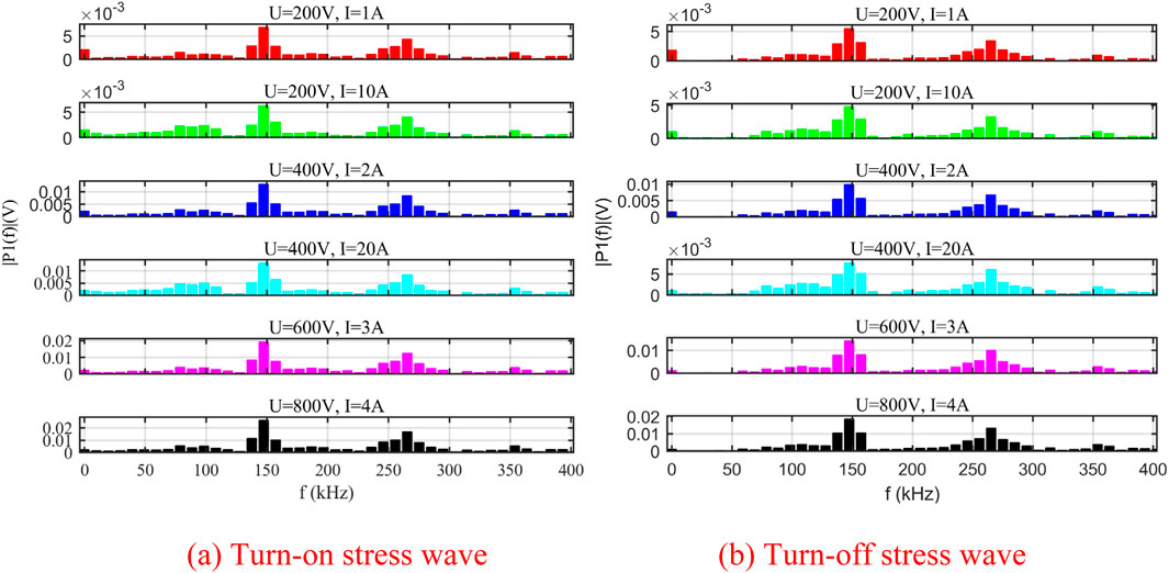
Figure 9. Spectra of stress waves under varying operating conditions. (a) Turn-on stress wave. (b) Turn-off stress wave.
4 Simulation analysis of stress wave propagation characteristics
The stress wave signals acquired experimentally are generated by chip vibrations and propagate downward through the solder layer to the DBC substrate before reaching the sensor. This transmission path may introduce attenuation and dispersion effects, meaning the detected signals do not fully represent the original vibration characteristics. To better approximate the root causes of chip vibration, it is essential to investigate the stress wave propagation process. We employ finite element simulation software to model the stress wave transmission within the SiC MOSFET power module. A two-dimensional simulation framework is established for the experimental module, enabling comparative analysis of waveform alterations as stress waves traverse the solder layer and DBC substrate.
4.1 Simulation setup
4.1.1 Model configuration
The 2D cross-sectional model of the SiC MOSFET power module is shown in Figure 10. Bond wires and terminals are omitted in the model due to their minimal impact on stress wave propagation toward the baseplate–these components reside within the encapsulant (low Young’s modulus) and would significantly increase computational complexity. The SiC MOSFET chip is soldered (0.1 mm solder layer) onto a DBC substrate, which consists of a top copper layer (0.3 mm), alumina ceramic plate (1.0 mm), and bottom copper layer (0.3 mm). To analyze signal transmission characteristics, two monitoring points are defined: Point A at the chip’s lower boundary and Point B at the bottom copper layer’s lower boundary. Material properties used in the simulation are listed in Table 2.
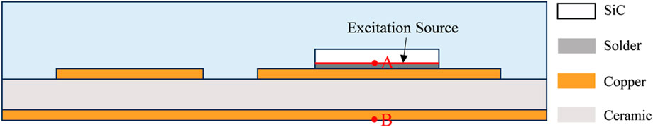
Figure 10. 2D simulation model of the SiC MOSFET power module.
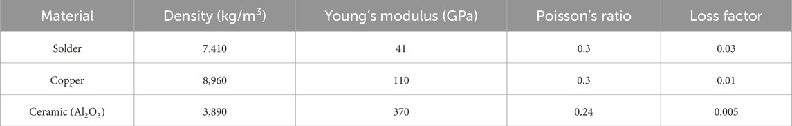
Table 2. Simulation parameters for each material (Zhang et al., 1993).
The finite element mesh configuration was governed by the one-sixth wavelength criterion to ensure accurate stress wave propagation modeling. Following the relation hmax < c/(6f), where c denotes material shear wave velocity and f represents the 600 kHz upper frequency limit identified through spectral analysis, theoretical maximum element sizes were calculated as 0.4 mm (solder, c = 1458 m/s), 1.7 mm (Al2O3 ceramic, c = 6193 m/s), and 0.6 mm (copper, c = 2173 m/s). To address geometric discontinuities while mitigating numerical dispersion artifacts, a globally conservative maximum element size of 0.1 mm was implemented.
4.1.2 Excitation source configuration
Two methods are employed to simulate stress wave propagation characteristics: (1) applying a stress load or (2) prescribing a displacement at the excitation source. The stress load method defines a specific stress waveform at the wave origin, while the displacement method specifies a displacement waveform. In this study, a stress load is applied to the lower boundary of the SiC MOSFET chip as the excitation source. The generation of stress waves in power devices originates from mechanical vibrations induced by rapidly varying electromechanical forces during switching transients. As demonstrated in Section 3.1, the oscillatory waveforms detected by the sensor exhibit individual cycles of approximately 5 μs. Accordingly, a Gaussian pulse (Figure 11) is adopted to model the transient stress excitation.
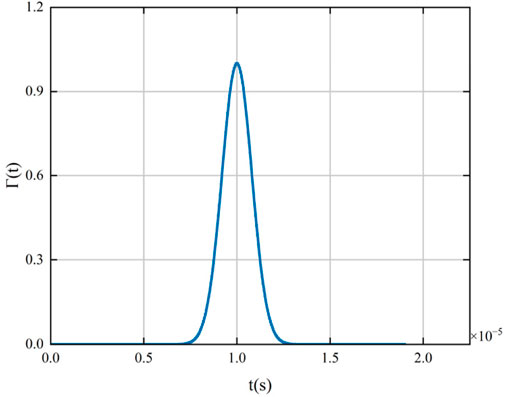
Figure 11. Gaussian pulse excitation source.
4.2 Simulation results and discussion
Figure 12 presents the time-domain and frequency-domain profiles of the σy stress component recorded at monitoring points A and B. In the time domain (Figure 12a), both locations exhibit nearly identical waveform shapes, characterized by a sharp Gaussian-like pulse. The peak amplitude at point B shows a 5.82% increase compared to point A. In the frequency domain (Figure 12b), the −3 dB bandwidth of the spectrum at point B is 5.88% wider than that at point A, with extended low-frequency components indicating slower spectral decay during propagation.
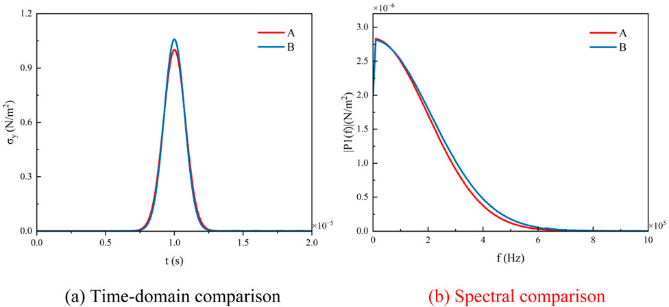
Figure 12. Y-direction stress component evolution at monitoring points A and B. (a) Time-domain comparison. (b) Spectral comparison.
This behavior can be attributed to guided wave propagation modes excited within the multilayer DBC structure. Due to the thinness of the ceramic substrate and the layered configuration, the stress wave likely couples into fundamental Lamb wave modes—specifically the A0 or S0 mode—within the copper-ceramic-copper sandwich. These guided modes, supported by the plate-like geometry, can exhibit constructive interference and enhanced energy transmission to the lower interface. The result is a slight amplification and spectral broadening at point B, where the wave maintains coherence and energy more effectively.
The numerical results confirm that defect-free solder and DBC layers introduce negligible distortion to stress wave propagation. The stress waveform observed at point B closely resembles the waveform near the excitation source, suggesting that it serves as a reliable proxy for the actual chip vibration signal.
5 Conclusion
This study systematically investigates the generation, propagation, and applicability of switching-induced stress waves in SiC MOSFET power modules for packaging health monitoring through combined experimental and numerical approaches. The principal conclusions are summarized as follows:
(1) Stress Wave Generation Characteristics: Both turn-on and turn-off transients in SiC MOSFETs excite mechanical stress waves, with time-domain waveform durations ranging from tens to hundreds of microseconds. Notably, despite opposite switching polarities, the two operational modes exhibit highly similar spectral distributions, featuring dominant peaks at approximately 150 kHz and 270 kHz.
(2) Electrical Parameter Effects: Increased bus voltage and load current enhance the time-domain amplitudes of stress waves, with voltage demonstrating significantly stronger modulation effectiveness than current. However, spectral characteristics (peak frequencies and distribution patterns) show minimal sensitivity to voltage/current variations.
(3) Propagation Path Analysis: Under defect-free conditions in the solder layer and DBC board, stress wave propagation induces only minor amplitude variations (5.82%) and spectral bandwidth expansion (5.88%). This confirms that the stress signals detected at the DBC substrate can faithfully represent the chip’s intrinsic vibrational behavior, providing a theoretical foundation for non-invasive packaging health monitoring.
Future research will focus on developing online detection methods for packaging defects (e.g., bond wire lift-off and solder voids) using switching-induced stress wave analysis and establishing quantitative correlations between mechanical signatures and chip-level stresses. To overcome the limitations of conventional power cycling tests—particularly their time-consuming nature and the concurrent degradation of multiple packaging components that complicates failure mode isolation—controlled test modules will be implemented. These include manually severed bond wires at predetermined locations and intentionally designed solder layer voids. This approach enables systematic analysis of stress wave parameter variations corresponding to specific failure modes, facilitating reliable defect characterization.
Data availability statement
The raw data supporting the conclusions of this article will be made available by the authors, without undue reservation.
Author contributions
SH: Data curation, Formal Analysis, Investigation, Writing – original draft. LF: Writing – original draft, Investigation. QH: Writing – original draft, Data curation. QN: Writing – original draft, Data curation. MS: Writing – review and editing. YM: Writing – review and editing.
Funding
The author(s) declare that financial support was received for the research and/or publication of this article. This study was generously supported by State Grid Corporation Headquarters Science and Technology Project: 5500-202399370A-2-2-ZB. The funder was not involved in the study design, collection, analysis, interpretation of data, the writing of this article, or the decision to submit it for publication.
Conflict of interest
Authors QH, QN, MS, and YM were employed by State Grid Shanghai Municipal Electrical Power Company.
The remaining authors declare that the research was conducted in the absence of any commercial or financial relationships that could be construed as a potential conflict of interest.
Generative AI statement
The author(s) declare that no Generative AI was used in the creation of this manuscript.
Publisher’s note
All claims expressed in this article are solely those of the authors and do not necessarily represent those of their affiliated organizations, or those of the publisher, the editors and the reviewers. Any product that may be evaluated in this article, or claim that may be made by its manufacturer, is not guaranteed or endorsed by the publisher.
References
Bai, Y., Shen, H., He, Y., Wang, L., Liu, F., Geng, X., et al. (2021). Analysis of the stress-wave influence parameters of silicon MOSFET under 300V drain source voltage. IEEE Sensors J. 21 (18), 20107–20118. doi:10.1109/jsen.2021.3094885
Brauhn, T., Sheng, M., Dow, B., Nogawa, H., and Lorenz, R. (2017). Module-integrated GMR-based current sensing for closed-loop control of a motor drive. IEEE Trans. Industry Appl. 53 (1), 222–231. doi:10.1109/tia.2016.2614771
Chen, C., Zhao, X., Zhou, B., and Gu, Q. (2013). Study on extracting crack fault feature of wind turbine blades. Proc. CSEE 33 (02), 112–117+20.
Dang, L. (2019). Study of health monitoring technology of metal structure based on PVDF piezoelectric sensor. Dissertation (Beijing: China University of Geosciences).
Davari, P., Kristensen, O., and Iannuzzo, F. (2018). Investigation of acoustic emission as a non-invasive method for detection of power semiconductor aging. Microelectron. Reliab. 88 (90), 545–549. doi:10.1016/j.microrel.2018.06.074
Ding, Y., Wang, Y., Sun, H., and Yin, Y. (2022). High-temperature partial discharge characteristics of power module packaging insulation under square pulse with high dv/dt based on down-mixing method. IEEE Trans. Industrial Electron. 70 (7), 7334–7342. doi:10.1109/tie.2022.3201276
Falck, J., Felgemacher, C., Rojko, A., Liserre, M., and Zacharias, P. (2018). Reliability of power electronic systems: an industry perspective. IEEE Ind. Electron. Mag. 12 (2), 24–35. doi:10.1109/mie.2018.2825481
Geng, X., He, Y., Li, Q., Tang, L., Wang, G., Liu, S., et al. (2023). Theoretical study on the generation of switching stress waves in power semiconductor devices. IEEE Trans. Power Electron. 38 (3), 3939–3950. doi:10.1109/tpel.2022.3225904
Geng, X., He, Y., Zeng, C., Wang, G., Liu, S., Yang, H., et al. (2022). Analysis of influence parameters of stress wave at the turn-off moment in IGBT device based on differential AE sensor. IEEE Sensors J. 22 (3), 2259–2270. doi:10.1109/jsen.2021.3134274
He, Y., Zou, X., Li, M., Zhou, Y., Zhao, Z., Huang, S., et al. (2021). Theoretical and experimental study on stress wave of power MOSFET under 30 volts. Proc. CSEE 41 (16), 5683–5693.
Jiang, G., An, L., and Yang, K. (2002). Numerical study of directionality patterns for acoustic radiation from a leak source on a heat-exchanger cylinder in boilers. Proc. CSEE 22 (06), 127–132.
Kärkkäinen, T., Talvitie, J., Kuisma, M., Hannonen, J., Ström, J., Mengotti, E., et al. (2014). Acoustic emission in power semiconductor modules—first observations. IEEE Trans. Power Electron. 29 (11), 6081–6086. doi:10.1109/tpel.2013.2295460
Kimoto, T. (2015). Material science and device physics in SiC technology for high-voltage power devices. Jpn. J. Appl. Phys. 54 (4), 040103. doi:10.7567/jjap.54.040103
Li, M., He, Y., Meng, Z., Wang, J., Zou, X., Hu, Y., et al. (2020). Acoustic emission-based experimental analysis of mechanical stress wave in IGBT device. IEEE Sensors J. 20 (11), 6064–6074. doi:10.1109/jsen.2020.2974312
Li, W., Chen, Y., Luo, H., Zhou, Y., Yang, H., and He, X. (2016). Review and prospect of junction temperature extraction principle of high power semiconductor devices. Proc. CSEE 36 (13), 3546–3557+3373. doi:10.13334/j.0258-8013.pcsee.160623
Li, W., Wang, Y., and Yin, Y. (2022). Review of packaging insulation reliability for high voltage power module. Proc. CSEE 42 (14), 5312–5326.
Maki, J., Akinaga, Y., Kozako, M., Hikita, M., Nakamura, Y., Taniguchi, K., et al. (2017). “Propagation characteristics of acoustic wave induced by partial discharge in IGBT module,” in 2017 International Symposium on Electrical Insulating Materials, Toyohashi, Japan, 11-15 September 2017 (IEEE), 668–671.
Müller, S., Drechsler, C., Heinkel, U., and Herold, C. (2016). “Acoustic emission for state-of-health determination in power modules,” in 13th International Multi-Conference on Systems, Signals and Devices, Leipzig, Germany, 21-24 March 2016 (IEEE), 468–471.
Ren, L., Wei, Z., Gong, C., and Shen, Q. (2015). Fault feature extraction techniques for power devices in power electronic converters: a review. Proc. CSEE 35 (12), 3089–3101.
Wang, X. (2014). Researches and applications of wide bandgap SiC power devices in electric vehicles. Proc. CSEE 34 (03), 371–379.
Wang, Y., Ding, Y., Yuan, Z., Peng, H., Wu, J., Yin, Y., et al. (2021). Space-charge accumulation and its impact on high-voltage power module partial discharge under DC and PWM waves: testing and modeling. IEEE Trans. Power Electron. 36 (10), 11097–11108. doi:10.1109/tpel.2021.3072655
Wen, H., Liu, Y., Jiao, D., Yeh, C., and Lai, J. (2021). “Design principles and optimization considerations of a high frequency transformer in GaN based 1 MHz 2.8 kW LLC resonant converter with over 99% efficiency,” in 2021 IEEE Applied Power Electronics Conference and Exposition (APEC), Phoenix, AZ, USA, 14-17 June 2021 (IEEE), 1939–1944.
Zare, F., Blaabjerg, F., Davari, P., Chang, G., and Adabi, J. (2019). IEEE access special section editorial: power quality and harmonics issues of future and smart grids. IEEE Access 7, 132803–132805. doi:10.1109/access.2019.2941666
Zhang, J., Perez, R., and Lavernia, E. (1993). Documentation of damping capacity of metallic, ceramic and metal-matrix composite materials. J. Mater. Sci. 28, 2395–2404. doi:10.1007/bf01151671
Zhou, H., Ma, G., and Zhang, M. (2019). Partial discharge ultrasonic signal detection technology in GIS based on the michelson fiber optic interferometer. Proc. CSEE 39 (21), 6452–6460.
Keywords: switching-induced stress waves, SiC MOSFET power module, finite element modeling, packaging health detecting, non-invasive detection
Citation: Huang S, Fan L, Heng Q, Ni Q, Sun M and Mao Y (2025) Characteristics and propagation of switching-induced stress waves in SiC MOSFET power modules. Front. Energy Res. 13:1623462. doi: 10.3389/fenrg.2025.1623462
Received: 09 May 2025; Accepted: 02 June 2025;
Published: 18 June 2025.
Edited by:
He Li, Berkeley Lab (DOE), United StatesReviewed by:
Wu Lu, Shanghai University of Electric Power, ChinaChen Zhou, The Pennsylvania State University (PSU), United States
Chunyang Li, Harbin University of Science and Technology, China
Copyright © 2025 Huang, Fan, Heng, Ni, Sun and Mao. This is an open-access article distributed under the terms of the Creative Commons Attribution License (CC BY). The use, distribution or reproduction in other forums is permitted, provided the original author(s) and the copyright owner(s) are credited and that the original publication in this journal is cited, in accordance with accepted academic practice. No use, distribution or reproduction is permitted which does not comply with these terms.
*Correspondence: Siqi Huang, aHVhbmdzaXFpQHNqdHUuZWR1LmNu