 Sana Basharat1,2
 Saeed Ehsan Awan2
 Rizwan Akhtar1,3*
 Alamdar Hussain2
 Shahid Iqbal4
 Sayyar Ali Shah1*Aihua Yuan1*
- 1School of Electronics and Information, Jiangsu University of Science and Technology, Zhenjiang, China
- 2Department of Electrical and Computer Engineering, COMSATS University Islamabad, Attock, Pakistan
- 3Department of Computer Science and Software Engineering, Pak-Austria Fachhochschule: Institute of Applied Sciences and Technology, Haripur-KPK, Pakistan
- 4Department of Electrical Engineering, University of Gujrat, Gujrat, Pakistan
DC–DC converters have wide applications in industries, motor drive circuits, electric vehicles, and power supplies. In traditional converters hard switching occurs due to switching losses. This imposes constraints on the converter’s efficiency which results in heat dissipation and reduction in the converter’s life. The proposed converter aims to encounter the hard switching problem with the provision of soft switching features. The presented topology is efficient with respect to the features of cost, compact size and durable lifetime of converter topology with the provision of low switching stresses. This research work proposes a novel stepdown converter with zero voltage switching characteristics. With the use of half bridge inverter switches and series resonant components in the auxiliary circuit, the target of zero voltage switching and reduction in switching stresses has been achieved. The proposed 500 W converter is designed to operate at frequency of 100 KHz with 300 V source input voltage. Output voltage of the converter is 150 V.
Introduction
Nowadays, the world is facing serious environmental concerns such as global warming and environmental pollution. Many factors are responsible for these immense climatic changes. One of those factors are the emission of harmful gases from traditional transportation systems. Researchers in power electronics are putting their efforts toward providing the most effective solution to cope with these challenges by the introduction of electric transportation systems. Revolution in the transportation sector for energy efficiency is increasing in today’s world. So, the development of electric vehicles has proliferated rapidly in recent years (Bose, 2010). The efficiency of electric vehicles depends upon many factors, of which the electric drive system is the most considerable one. For an efficient and optimal electric vehicles system, the electric drive system should be designed optimally to ensure fewer losses (Martinez et al., 2016). The motor drive system consists of electric motor, power converter, controller, and different sensors. The efficiency of the motor drive system mainly depends upon the power converter used in it. DC–DC converters have wide applications in industries, PC power supplies, and processor IC’s (Integrated Circuits) (Marchesoni and Vacca, 2007; Batista et al., 2009). These power converters operate with hard switching which causes switching losses that result in a reduction in efficiency of the converter. Hard switching occurs due to the presence of the current and voltage across the switch during its transition state. The researchers put their efforts toward encountering the problems of hard switching by the provision of soft switching techniques. In this paper a novel topology of DC–DC converter operating in ZVS (Zero Voltage Switching) condition is proposed. The converter is implemented in ORCAD/PSPICE (Oregon Computer Aided Design/Personal Computer Simulation Program with Integration Circuit). The result comparison was carried out with the previous research works which proves the efficiency of the proposed work in terms of cost, size and ratings of high input voltage/output voltage conversion ratio.
Related Work
The demand of more efficient DC–DC power converters has increased due to their wide applications in industries. The conventional converters face the problem of hard switching during the transition state of the switches. Ideally, when the switch gets turned on, voltage across it should be zero. Similarly, at the turn off state, the current should be zero. But practically, the situation goes on differently due to the presence of voltage and current across the switches. It imposes power losses and stresses on the switch, thus causing reduction in the switch’s life and leads towards a less efficient system.
Thus, the requirement of lossless and efficient dc-dc converters pushes researchers to introduce new topologies for reduction in switching losses, as the conventional dc–dc converters do not exhibit the soft switching features and techniques, so different researchers have invented new topologies to encounter hard switching. This section covers the related work on buck converter with the comparative analysis on soft switching techniques. Many researchers have used different soft switching techniques on buck converters with the introduction of new topologies.
Moschopoulos et al., (1999) introduced a stepup converter with ZVS technique for low stresses across the switches. It was designed for low power applications. Its Peak switch stresses are slightly higher than the conventional ones. It involves the use of transformer which also leads toward the complexity and core losses. Kumar et al., (2017) used a ZVS technique to improve the efficiency of the DC–DC converter for both isolated and non-isolated converters. It is a 35 W power converter working for low voltage rating. The topology has less stepdown ratio with a greater number of components used in it. Soft Switching techniques with the characteristics of losses reductions were also introduced for bidirectional buck-boost converter. Broday et al., (2016) and Hussain et al., (2019) proposed the topologies for reduction in losses and provision of soft switching characteristics for bidirectional converters. The main drawback is the factor of complexity and cost due to the use of a tapped inductor and design of magnetic core in the topologies, causing increment in cost. Lin et al., (2008) introduced a Buck-fly back converter for a ZVS operation using the topology of the active snubber circuit. This 240 W power converter with 90 kHz switching frequency provides a large voltage stepdown between input 140 V and output 24 V. The circuit has its limitation due to the use of a greater number of components in it. Furthermore, a novel ZVS topology used by Zhao (2011) to encounter the problem of the narrow duty cycle and hard switching of the conventional converter. The prototype is 48V1V with 100 kHz switching frequency. Although the topology is simple, but its voltage conversion ratio is very low. Chauhan and Pandey (2017) put his effort into reducing switching losses and minimizing hard switching problems by comparison of the conventional buck converter with the proposed topology. The topology is simulated in PSIM with specifications of a 12 V/4.8 V DC–DC converter with a 50 MHz switching frequency. This topology is designed just for low power applications i.e battery charging applications. Striney et al., (2016) proposed a ZVS topology of Buck converter for multiload applications. It encounters the problem of cross regulation parameters in case of multiload applications to reduce switching losses. The circuitry is complex due to the use of the motor which leads toward the cost increment and power losses as well as rotary losses associated with motors. Marvi et al., (2016) presented a technique to improve the overall efficiency of the voltage regulator module. It also provides ZVS across the main switch in the isolated converter. In the isolated converter, with the use of the transformer, the situation leads toward the more complex and costly circuits as well as bulky size of converters. Another ZVS buck converter topology for a bidirectional buck converter is described by Song et al., (2014). It has applications in hybrid energy storage systems. The topology is capable of providing low losses with ZVS features and constant frequency. The complexity of a high stepdown operation circuit causes a reduction in efficiency and increases design difficulty and cost. A low duty cycle causes problems of insufficient PWM (Pulse Width Modulation) resolution which causes inappropriate control to the converter. Yeh et al., (2017) encounters the problem of a low duty cycle by using a tapped inductor buck converter which extends duty cycle. In contrast to the traditional converter technology, the presented converter works with a much wider duty cycle with same voltage level conversion ratio. The circuit topology is not complex and is simple, but it operates on a low power rating. Lakshminarasamma and Ramanarayanan (2007) presented Quasi resonant technology for the efficient DC–DC converter with the use of a couple inductor. It results in lossless switching across both the switches (main and auxiliary) without affecting the V/I rating of main device. A converter with 33 W and 400 kHz frequency is simulated in this paper. The limitation of this topology is that it has high voltage and current stress across the switch. The ZVS introduced in this paper works with the switch with the same VA ratings as the source voltage and load current, but it failed to overcome the problem of switching loss across the auxiliary switch in the case of the turn off state. Various researchers (Do, 2011; Kollimalla et al., 2014; Babaei and Saadatizadeh, 2019) described a bidirectional Buck–Boost technology for the operation of a ZVS DC–DC converter. In the converter the inductor LL provides ZVS operation and increases the efficiency of the circuit. It encounters all the problems of the reverse recovery phenomena of body diode of the switches. These converters exhibit additional windings across the inductor which causes complexity due to the use of a greater number of components. Tsai et al., (2011) described topology as a provision of ZVS topology for an active clamp circuit in the interleaved buck converter. The topology introduced by Wang et al., (2011) encounters the problem of leakage energy and ringing voltage across the active switches including the use of the auxiliary switch and coupled inductor for ZVS operation of the PWM buck DC–DC converter. Hwan Oh, (2008) introduced ZVS topology for light load conditions for the synchronous rectifiers buck converter. In this technology the output diode gets replaced by the MOSFET (Metal Oxide Semiconductor Field Effect Transistor) which ensures fewer conduction losses with improved efficiency. The topology consists of 12 V/5 V voltage ratings with 25 W power and switching frequency of 100 kHz. Other than the light load, it is also necessary to provide ZVS for a full load. Shao et al., (2017) proposed ZVS topology suitable for both light and full load conditions. It minimizes conduction losses in switches during a continuous conduction mode with the use of additional L and C components with a conventional buck converter. Kanamarlapudi et al., (2017) presented the ZVS full-bridge DC-DC converters. The prototype is a 2 KW power converter with voltage conversion ratings of 300 V/200 V and a switching frequency of 20 kHz. Most of the converter topologies described in this section are designed for low power applications with a lower voltage conversion ratio. So, it is very necessary to provide soft switching for high power applications with high voltage ratings. Kim et al., (2019) proposed converter which removes the problem of hard switching from the rectifier. Its main advantage is lesser component count; however, transformer incorporation may cause additional losses. An auxiliary winding turn base converter was proposed by Lin (2020). The proposed converter was designed for a wide input range of voltages. It has a high number of components and the switch undergoes a hard operation. The Research Community has exploited the topology of ZVS along with PWM in auxiliary type circuits for different applications (Kim et al., 2019; Marikkannan et al., 2019; Srivastava et al., 2019; Lin, 2020).
The limitations of research work are that the topology is presented with software simulation in PSPICE. Zero voltage switching is shown graphically. In terms of hardware implementation, the topology will be costly as it has a greater number of components used in it. The converter is limited for applications up to 500 W. The converter, due to having a greater number of components, increases its complexity and cost factor.
The proposed converter in this paper is beneficial in terms of working on high voltage ratings. All the stated topologies in the literature review have worked on low voltages. In comparison with the others, this topology provides ZVS for high voltage ratings.
It encounters the problem of hard switching by providing zero voltage switching which ensures zero power losses across the main switch.
The contributions of the research work are mentioned below:
• In switching mode, the converter provides zero losses across main switch Sm, Dynamic losses across the witch will be zero but static losses due to resistor will be there.
• With the use of an auxiliary circuit, it encounters hard switching problem by providing soft-switching across the switch.
Proposed ZVS DC–DC Converter
The proposed Zero Voltage Switching Pulse Width Modulation DC-DC Buck converter with a Voltage Doubler Type Auxiliary Circuit is presented in Figure 1. The circuit consists of two parts: 1) Main circuit 2) Auxiliary circuit. The main circuit consists of the voltage source Vin, main switch Sm, main inductor L0, output capacitor C0, and output resistor R0. The auxiliary circuit consists of the half-bridge inverter switches i. e auxiliary switches S1 and S2, two diodes D1 and D2, and resonant components Lr and Cr.
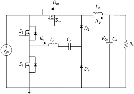
FIGURE 1. ZVS PWM buck DC–DC converter with voltage doubler type auxiliary circuit.
The output of the half-bridge inverter is connected to the series LC resonant circuit. The output of the resonant circuit is connected to the main inductor L0 through D1 and D2. The main switch Sm is the same as the conventional Buck Converter switch. It is placed between the input voltage source and main inductor L0. The output capacitor C0 is connected across the output resistor R0.
Principle of Operation
Mode Analysis
The proposed converter operation is divided into six modes depending on the working of the converter. The key steady-state waveforms of the converter with the division of modes are shown in Figure 2. Each mode of current is explained with the help of an equivalent circuit diagram and key steady-state waveform.
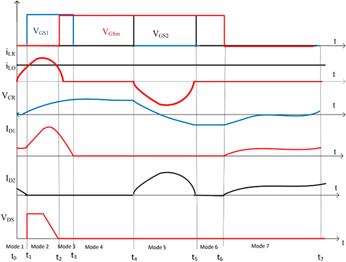
FIGURE 2. Key steady-state waveform of the converter.
Equivalent Circuits of Operation modes
The equivalent circuits of operation modes of the proposed converter are shown in Figure 3.
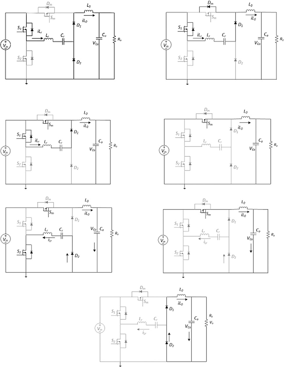
FIGURE 3. Operation modes of the proposed DC–DC buck converter.
Mode 1: (Interval t0 < t < t1)
Mode 1 begins at time t = t0. At this time interval, the equivalent circuit diagram of the converter is shown in Figure 3A. The switching cycle begins at time t0. Before t0 the main and auxiliary switches are turned off and the main inductor is in a conduction state, thus providing energy to the circuit. This mode starts at the time to when the main inductor Lo is connected with the source through the resonant path. The main inductor current iLo is rising from the minimum value. Current through resonant inductor Lr rises which causes resonant capacitor Cr to charge. Diode D1 and D2 are forward biased due to the previous state. Output voltage Vo is maintained through capacitor Co.
During this mode, the resonant inductor current ILr is less than the main inductor current as it can be seen in Figure 2. Diodes are forward biased due to the energy provided by the main inductor L0. This mode will continue until the currents of resonant and main inductor become equal.
The voltage and current across the inductor “L” will be:
Mode 2: (t1<t < t2)
This mode begins at t1 when both the currents become equal i: e resonant inductor current and main inductor current. The body diode of the main switch Sm is turned on and D2 is turned off. The resonant inductor current iLr keeps on swinging sinusoidally. The resonant current exceeds iLo therefore D2 turned off and D1 remains forward biased. Once Dm is turned on the main switch can be turned on with ZVS.
In this mode, when both currents become equal, Dm gets turned on, and the potential difference across the main switch becomes equal thus ensuring zero voltage across the main switch. It provides zero voltage switching phenomena in the converter.
The circuit diagram for mode 2 is shown in Figure 3B. The current passing through diode D1 divides into two paths. One is from the body diode of the main switch. Another path is provided by the main inductor. Output Capacitor Co maintains the constant output voltage V0.
The current and voltage equations for mode 2 are as follows:
Mode 3: (t2<t < t3)
Figure 3C shows the equivalent circuit diagram in the case of mode 3. This mode begins when the main switch Sm is turned on. In this mode, Sm is turned on with ZVS. The current through the resonant path falls down linearly. The capacitor Cr is charged to the maximum value and goes to a steady state. In this mode, S1 will also be turned off. Current through inductor Lo is increasing continuously. During the on time of Sm, the circuit behaves like a conventional buck converter. This mode ends when auxiliary switch S2 gets turned on. The equations for this mode are just like the conventional buck converter mode.
Mode 4: (t3<t < t4)
This Mode begins at time t = t3. In this mode when S1 gets turned off so the main switch Sm is just in a conduction state. This time is the delay time for the auxiliary switch S2. The current through the resonant path is zero in this state. Both diodes are reversed biased in this mode. The source is connected to the load with the help of the main switch Sm. The equivalent circuit diagram for this mode is shown in Figure 3D. This mode ends at time t = t4.
Mode 5: (t4<t < t5)
In this mode the main switch Sm and auxiliary switch S2 are turned ON. The equivalent circuit diagram showing the path of the current flows in this mode is shown in Figure 3E. Sm provides the conventional buck converter operation in the circuit. During this mode, the energy stored in the capacitor gets released in the closed loop followed by the auxiliary switch S2, diode D2, and resonant inductor Lr. When S2 is turned on, the resonant capacitor Cr starts discharging due to the fall of current through the resonant inductor Lr. Diode D2 becomes forward biased. Current flows through the resonant loop until the switch S2 is turned off.
Mode 6: (t5<t < t6)
This mode starts at time t5 when auxiliary switches S1, S2 are turned off. In this mode, only the main switch Sm is in a conduction state. The circuit in this mode acts as a conventional buck converter. The current loop consists of main switch Sm, output inductor Lo and capacitor C0. Current through the load inductor Lo rises and provides constant output voltage through capacitor C0.Figure 3F shows the equivalent circuit diagram in this mode.
Mode 7: (t6<t < t7)
Figure 3G shows the equivalent circuit diagram of mode 7. This mode begins at t = t6. As all the switches are in an off state in this mode. Output main inductor Lo provides energy to the circuit. The current flows through the output capacitor and two diodes D1 and D2. This mode ends at time t = t0 when S1 is turned on. The equations of the current across the diodes in this mode are as follows:
Gain Analysis
The gain analysis of the converter is just similar to the conventional buck converter gain. The principle of the inductor volt sec balance is used to determine the gain analysis of the converter. According to it, the average or dc component of the voltage applied across the inductor must be zero. When the main switch is closed the analysis for gain is described here.
The above equation describes the gain of the buck converter. From the equation, it is cleared that output voltage V0 depends upon the input voltage Vin and duty cycle D.
Duty Cycle Limitation
The output voltage of the buck converter depends upon the input voltage Vin and duty cycle D.
Compared with the conventional buck converter, duty cycle D is ranging from 0 to 1. The Dmin for the auxiliary switch is 10% of D. So, the duty cycle range becomes
As in the presented topology, the value of D cannot be zero so it leads toward a new duty cycle range from minimum value to 1.
The equation shows that the duty cycle value is ranging from its minimum value (0.1) to 1.
Design and Implementation
This section explains the designing and Implementation procedure of the proposed converter. The components used in the circuit implementation are selected on the basis of 500 W load operating at 150 V as listed in Table 1.
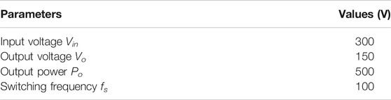
TABLE 1. Specifications of the proposed DC–DC converter.
Referred to the data mentioned in Table 1, the basic parameters for the designing of the DC–DC converter are calculated here. It includes output current Io, output resistor Ro, switching time period Ts. The value of the load resistor Ro of the DC–DC converter is calculated as:
The conventional buck converter has filter inductor Lo at the output side. It provides the continuous and smooth output current waveform at the output load terminal of the converter. The output inductor current is determined as:
From the given switching frequency, the total time period of the circuit can be found out. The time period and frequency are inversely proportional to each other. With the known information of one parameter, we can find out the value of the other.
Design of the Converter
This section covers the designing of the parameters of DC–DC converter topology. The DC–DC converter with the ZVS technique is designed for a practical application of 500 W. The topology consists of two sub-circuits, the main and auxiliary circuit. The parameters to be designed in the main circuit includes the main inductor Lo and output capacitor Co. The designing of the auxiliary circuit includes resonant inductor Lr and resonant capacitor Cr. The converter is operating in continuous conduction mode.
Determination of the Duty Cycle
The output voltage of the buck converter depends upon the input voltage Vin and duty cycle D.
From the output and input voltage values the duty cycle of the circuit can be found as:
Output Inductance Lo
The next step is to determine the size of the main inductor L0 of the converter. The inductor is a wire wrapped around the ferromagnetic material known as the core. Lmin is the minimum value of the inductor at which the converter operates for continuous conduction mode. In the design process, such value of the inductor should be chosen which is greater than the Lmin.
Lmin is the minimum inductance value required for continuous current. For the converter’s design, the value of inductor L0 should be greater than or equal to Lmin. The value of inductor L0 depends upon the switching frequency, output and input voltages Vin and Vout, duty cycle D, and peak to peak variation in the inductor current. The formula of determination of inductor value L is:
Assume that ΔiL is 20% of load current.
Putting this value in above equation.
The above equation describes the value of main inductance L0 for a specified peak to peak inductor current for continuous-current operation of the converter.
Output Capacitance Co
The value of output capacitance Co can be found out by the following formula.
Assume that
Putting the value of
The above equation shows the values of output capacitor Co to be used in the converter. Capacitor C0 provides the continuous output voltage value. The high value of capacitance minimizes the output voltage ripples.
Resonant Inductor Lr and Capacitor Cr
The selection of resonant capacitance Cr and inductance Lr is the most important step in the designing of the power converter. As, both the auxiliary switches turned on for a time of less than 1 µs so, from total time Ts = 10 µs, assume that 10% of the total is dedicated to two auxiliary switches.
In the above equation, assume the value of resonant capacitor Cr = 10 nF and, simplifying the above equation, the value of resonant inductor Lr can be found.
Equation (56) defines the range of values for the resonant inductor. By adjusting the values of resonant inductor and capacitor values the required behavior of the resonant current can be achieved. From the above values of the resonant inductor Lr and resonant capacitor Cr, resonant frequency fr of the auxiliary circuit can be found as:
fr can also be found through using the relationship with the switching frequency fs.
The impedance of the auxiliary circuit Zr can also be found as.
By putting values:
Power Loss Analysis
In the proposed converter, due to zero voltage switching during the transition state of the switches, switching losses goes to zero, as the drain to the source voltage of the main switch Sm is zero in this converter. So, power loss across the switch goes to zero. Dynamic losses across the switch are zero. But static losses exist due to the resistance factor.
Power losses across the switch can be calculated as,
where p = power, Vds = drain to source voltage, Rdon = Static drain to source on resistance.
From the datasheet of used MOSFET in the designing of converter the value of Rdon is found as 0.55 Ω. As Vds is zero at the transition state of the switch so, power loss across the switch goes to zero. Thus, verifying zero voltage characteristics of the converter.
Simulation Results
The simulation results of the soft-switching topology are discussed in this section. The ZVS operation of the PWM Buck converter can be verified with a voltage waveform across the main switch. The circuit diagram of the proposed converter which was presented in the previous section is simulated in PSPICE. In Figure 4 the software simulated circuit is shown.
FIGURE 4. PSPICE Circuit simulation.
The results verify the gain analysis of the step-down converter. It also verifies the ZVS characteristics of the proposed topology. The simulation results of current and voltage of resonant components, main inductor current, main capacitor voltages, and diode currents are also discussed in this section.
The simulated converter is 500 W with an input voltage of 300 V. The switching frequency is 100 kHz.
Voltage Gain Analysis
Figure 5 is the output voltage simulated result graph operating with a 50% duty cycle. It can be seen in the figure that it has two plots in it. Blue colored waveform shows the plot for an input voltage of 300 V. The output voltage plot verifies the derived relation from Eq (22) which is 150 V is shown with pink colored waveform. Switching frequency directly affects the output voltage. Changing the switching frequency effects D thus result in a change of the output voltage.
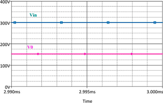
FIGURE 5. Input and Output Voltage Waveform of Converter. simulation result verifies the operation of the buck converter with the magnitude less than the input voltage. It converts 300–150 V.
Gate Signals of the Power Switches
Gate signals provided to the converter are shown in Figure 6.
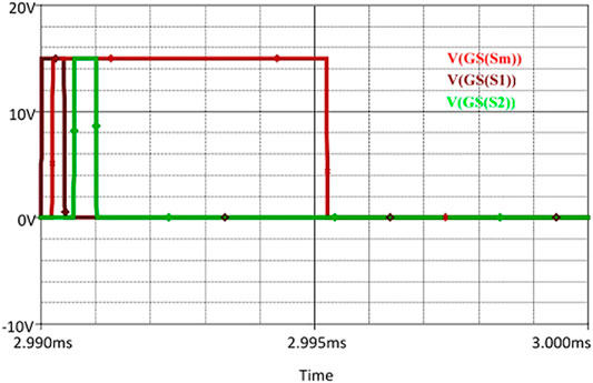
FIGURE 6. Gate Signals of Power Switches used in Converter.
Gate pulses are fed as input to the half-bridge inverter switches and the main switch at the gate to the source terminal of the switches. The Pulse Width Modulation technique is used to control the load voltage. The converter is operating with a 50% duty cycle. In the presented topology, three power switches are used. One main switch and two auxiliary switches. Gate signals are provided to the switches for controlling their on/off states. A V pulse is used in the circuit for pulse generation in PSPICE. It involves different parameters that need to be set for the required output. Before the on state of the main switch, S1 of the auxiliary circuit gets turned on. Sm turned on with a delay of 0.2 µs. In Figure 6, Maron colored waveform is the gate pulse for S1. After a delay of 0.6 µs, the auxiliary switch S2 gets turned on. It is shown as a green-colored waveform. Both the auxiliary switch remains turned on for 2 µs. The red-colored waveform is the gate pulse of the main switch Sm. It remains turned on for 5 µs. The duty cycle of the converter will remain the same throughout the operation of the converter for the respective value of input and load voltage.
Analysis of the Currents of Resonant ILr and Main Inductor Io
The simulation waveform for the resonant inductor current ILr and the main inductor current Io is illustrated in Figure 7.
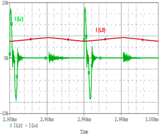
FIGURE 7. Current waveform of ILr and I0.
From Figure 7, the behavior of resonant inductor current can be seen as sinusoidal in nature. While the DC current flows through Lo. Equation (65) describes the average dc current through the main inductor which is also the output current of the converter.
ILr flows through the auxiliary circuit. The behavior of ILr can be explained through two cycles. In positive half cycle switch S1 gets turned on, ILr rises linearly from 0 to peak value. Both ILr and Io become equal at I0 = 3 A. After this zero crossing, the main diode Dm gets turned on. During this interval, the main switch Sm can be made to turn on in that portion at any time before the second crossing of both currents. This enables the ZVS of the converter across the main switch. After the second crossing of both currents again ILr becomes less than Io. When ILr reaches zero it stops the flow of current.
In the negative half cycle, as shown in the above waveform, ILr flows through the resonant tank followed by the D2, S2, and resonant capacitor. The peak and rms value of the resonant current is described in Equations (66) and (67). The Resonant Inductor current has its peak value in the case of a negative half cycle of −7 A.
As the resonant inductor current waveform is sinusoidal in nature, the total area of the waveform remains the same in both the cycles. In the first half cycle, the waveform is steeper and narrower. In comparison with the negative half cycle, the waveform is wider with a low peak. According to the volt sec balance of inductor, the area under the curve in both half cycles must be equal. Figure 8 is in accordance with the volt sec balance of the inductor.
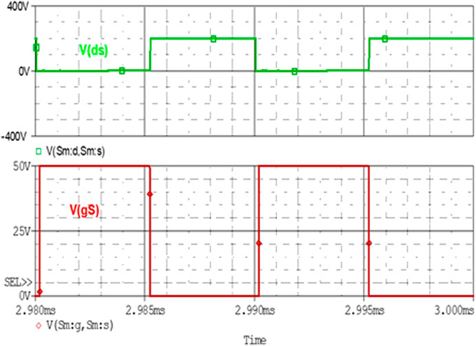
FIGURE 8. Zero voltage switching graph.
The ringing effects shown in the waveform of Figure 8 are unwanted parts. These are due to parasitic effects. Due to the reverse recovery effects of diodes, these portions emerge in the waveform. These unwanted effects can be removed by using the best quality diodes and components in hardware implementation. In software designing, the converters face this type of problem.
Analysis of Zero Voltage Switching Operation of the Converter
Achievement of zero voltage switching is the focus of this topology. It can be viewed and verified in Figure 9. As for ZVS operation, the most necessary parameter is that the drain to source voltage VDS should be zero across the switch before the gate pulse is applied. So, Figure 9 verifies this operation by seeing that when the gate pulse is applied across the main switch Sm, VDS is zero across the switch. In the above diagram, the green-colored waveform shows the VDS across the main switch. During the positive half cycle when iLr becomes equal to Io, then iLr flows through the body diode Dm of main switch Sm. It makes diode Dm forward biased. Figure 10 shows the current across the main diode.
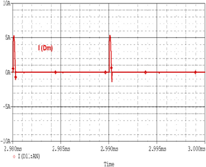
FIGURE 9. Current through the body diode of the main switch.
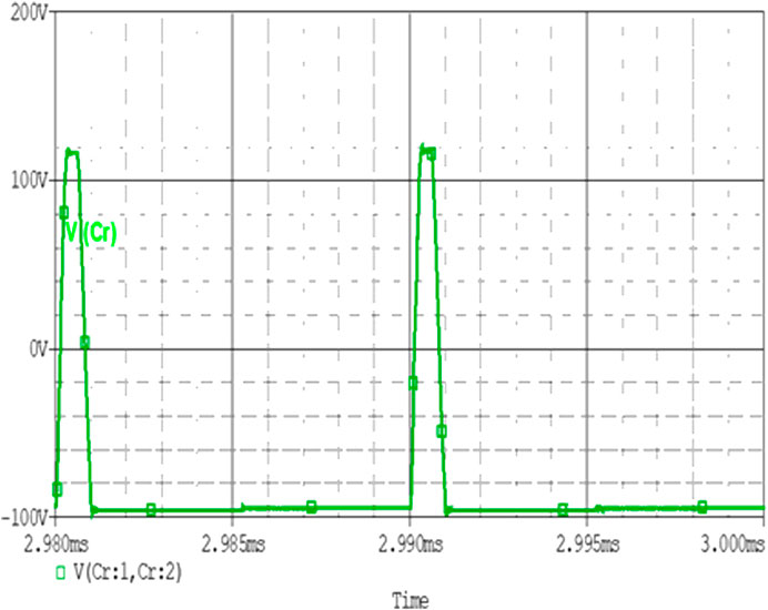
FIGURE 10. Voltage waveform across the resonant capacitor.
Analysis of Zero Voltage Switching Operation of the Converter
As shown in Figure 8, the combined effect of the main inductor current and resonant inductor current flows across the body diode of the main switch. It has a peak value of 5.283 A.
When the current through diode Dm goes to zero then VDS also reaches zero. Switch Sm becomes active through gate pulse VGS with no power loss across the switch. The nature of IDm is also sinusoidal as iLr flows across it.
Conventionally, power is absorbed across the switching devices during their turn on or turn off time. This is due to the fact that current or voltages across it is non-zero during the transition. These transitions occurred rapidly when working with high frequency. To eliminate these losses resonant converters are used. They provide soft-switching across the switches during their transition. During turn on/turn off the switches, voltage, and current become zero. It results in zero power absorption across the switches. In ZVS operation when the switch gets turned on, the voltage across the switch reaches zero. Thus, ensuring zero power loss. From the given waveforms, it can be clearly verified that the proposed converter ensures zero voltage switching.
Analysis of Resonant Capacitor Voltage Vcr
The analysis of the behavior of voltage across the resonant capacitor is explained in this section. In the resonant tank, the capacitor and inductor both are in series. The waveform of voltage across the capacitor is shown in Figure 10. The resonant inductor current ILr affects the behavior of voltage across the resonant capacitor Cr. In the positive half cycle of the sinusoidal current waveform, when the resonant inductor current ILr rises linearly, the positive voltage builds up across the capacitor. The capacitor voltages start building up from the previous value that is from −98 A. Voltages go on increasing until its peak value 118 V. Until this point, the resonant inductor current falls down to zero due to the turned off state of S1. The capacitor goes on to a steady state for the shortest time period of delay for S2.
As soon as S2 is turned on, the capacitor starts releasing energy to the auxiliary circuit thus at the turned-off time of S2, all the energy gets released thus flowing current in the closed loop. The capacitor voltage increases until ILr flows through it. As soon as ILr becomes less than Io the resonant current stops flowing the loop. At that point, the capacitor voltage reaches its maximum value.
In the negative half cycle of the resonant current, the capacitor acts as a source releasing its energy in this loop. When ILr reaches zero crossing the capacitor discharges at its negative maximum value and goes to a steady state.
Analysis of Current Across Diode D1 and D2
The waveform of the current across the diode D1 and D2 are shown in Figures 11 and 12. The currents across diodes D1 and D2 are explained in accordance with the resonant and main inductor current. When all switches are turned off, Io is greater than ILr so, Io flow through diodes D1 and D2. At this time 3.072 A current flows across both diodes.
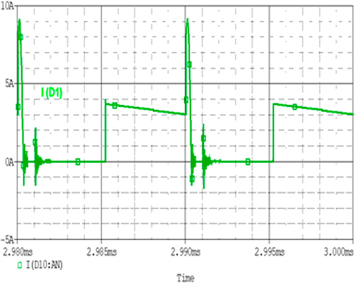
FIGURE 11. Diode D1 Current Waveform. When S2 turned on then diode D1 gets reversed biased and D2 gets forward biased. Figure 12 shows the current through diode D2.
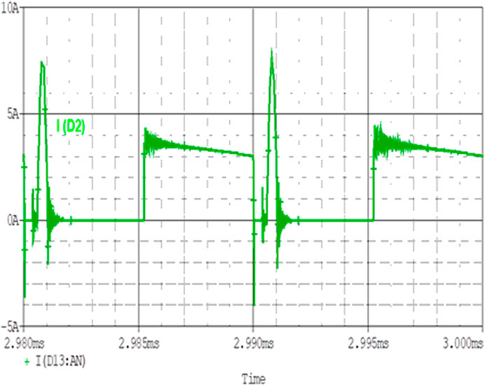
FIGURE 12. Diode D2 current Waveform.
When S1 is turned on, ILr rises linearly. After the point when Io and ILr become equal, ILr flows through the diode D1. D2 is reversed biased. Peak and rms values of current flowing through diode are described in Eq (69).
ILr flows through the diode D2, which has a peak value of 7.5 A. The nature of the waveform is sinusoidal with just a positive cycle. It has an rms value of 3.6640 A.
When all switches get turned off, then output inductor Lo releases energy in the form of current Io. Diodes D1 and D2 provide a path to the current. At this time average current of 3.57 A flows through both diodes. So, during the conduction period of switches ILr flows through diodes, and during the off period, Io flows through diodes.
Analysis of Zero Voltage Switching for Different Input and Output Values
The topology is efficient and provides zero voltage switching for different values of input and output voltage. Here is the analysis of ZVS achievement for different values. More results in Figures 13–20 are presented in this section with the help of simulated waveforms.
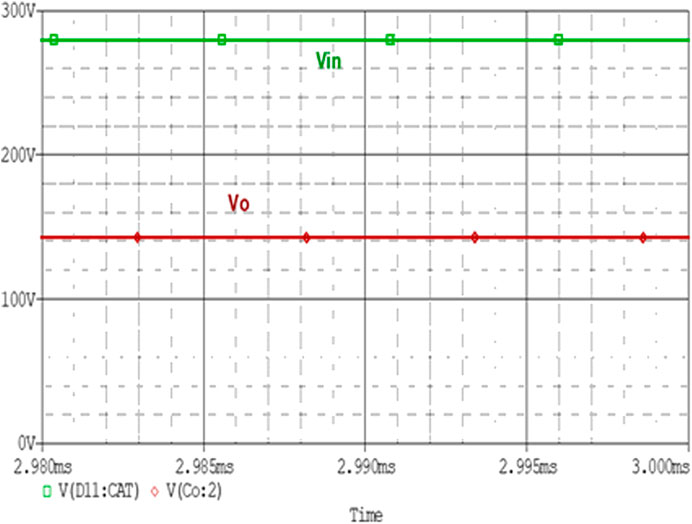
FIGURE 13. Input and Output Voltage Waveform of Converter.
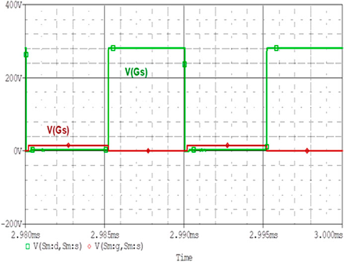
FIGURE 14. Zero voltage switching graph.
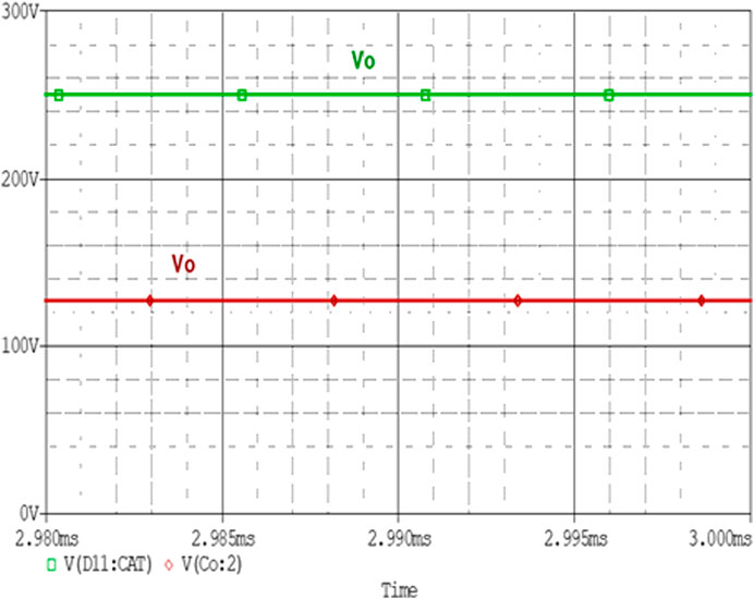
FIGURE 15. Input and output voltage waveform of converter.
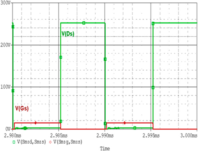
FIGURE 16. Zero voltage switching graph.
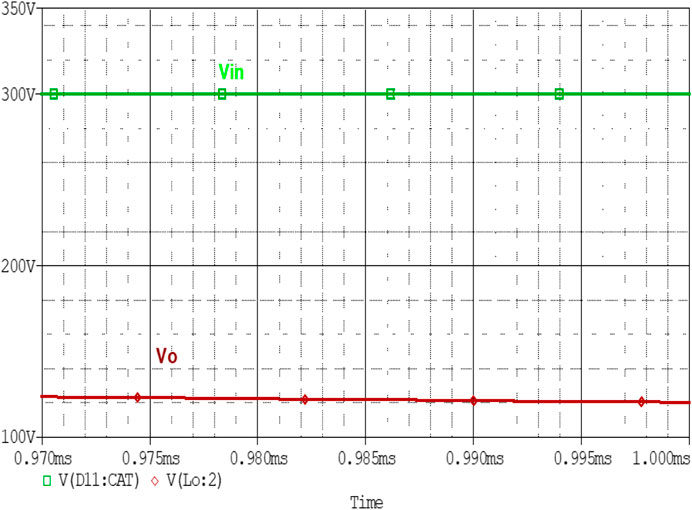
FIGURE 17. Input and output voltage waveform of converter.
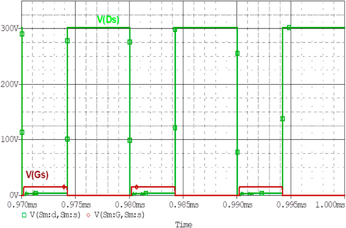
FIGURE 18. Zero voltage switching graph.
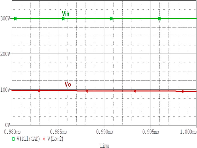
FIGURE 19. Input and output voltage waveform of converter.
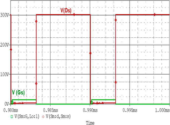
FIGURE 20. Zero voltage switching graph.
The converter provides ZVS for the above values too. The figure describes the ZVS achievement of the converter for these values with a duty cycle of 50%.
The above simulated results clearly verify the achievement of ZVS for different input-output voltage values and duty cycles. It can be seen that in all cases the circuit provides zero voltage switching. It provides zero switching losses across the switch during the transition state.
A comparison of the proposed research topology can be clearly illustrated from Table 2.
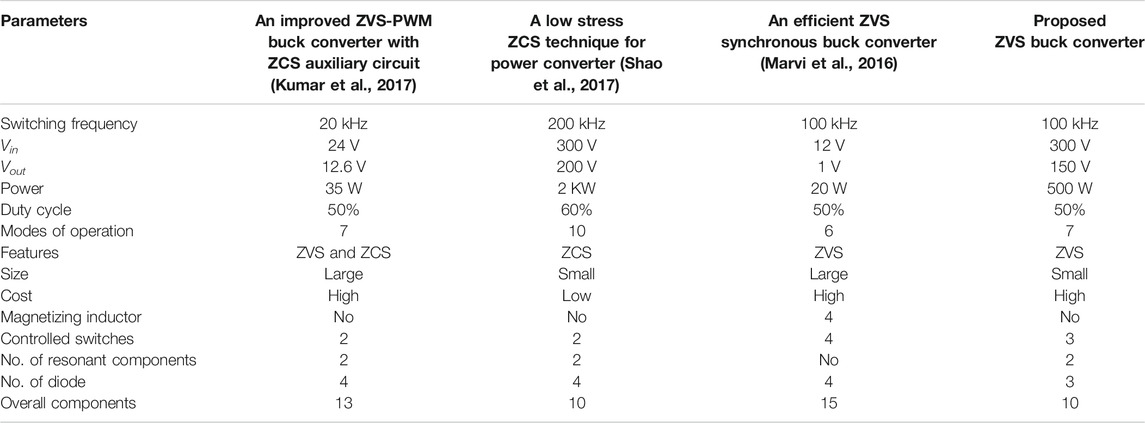
TABLE 2. Result comparison of proposed topology with previous circuits.
Conclusion
A novel ZVS based DC–DC converter with an auxiliary circuit has been proposed in this work. The proposed converter encounters the hard-switching problems of the conventional converter during its transition modes. To keep away the dynamic power losses across solid-state devices an auxiliary circuit consists of MOSFET and resonant components is incorporated with the conventional buck converter. Keeping in view for the application of the 500 W system the parameters and components have been designed optimally. The verification of the design has been made in PSPICE/ORCAD. The novel topology is simulated with voltage ratings 300/150 V, a duty cycle of 50%, and 100 kHz frequency. ZVS across the main switch Sm has been achieved during the transition mode of the converter and is shown graphically. Thus, the converter provides zero voltage switching for high voltage ratings. The reduction of stresses in the research work is shown graphically with the help of zero voltage switching waveform across main switch Sm.
In the future this work can be extended to be designed for electric vehicles to interface the elements for a power train. As the converter works for high voltage ratings, it can also be implemented in dc motor drives of electric vehicles.
Data Availability Statement
The raw data supporting the conclusions of this article will be made available by the authors, without undue reservation.
Author Contributions
All authors listed have made a substantial, direct and intellectual contribution to the work, and approved it for publication.
Funding
This work is supported by the National Natural Science Foundation of China (NSFC) under Grant Number 61771225.
Conflict of Interest
The authors declare that the research was conducted in the absence of any commercial or financial relationships that could be construed as a potential conflict of interest.
Nomenclature
Co: output capacitor
D: duty cycle
D1: diode 1
D2: diode 2
Dm: main diode
f: frequency
H: henry
Ip: peak current
Ro: output resistor
S1: switch 1
S2: switch 2
t: time
Tr: resonant time
Ts: switching time
V: voltage
VGS1: gate pulse voltage of S1
Vin: input voltage
Zo: output impedance
Zr: resonant impedance
References
Babaei, E., and Saadatizadeh, Z. (2019). A new interleaved high voltage gain bidirectional buck-boost DC/DC converter with capability of zero voltage switching. Elec. Power Compon. Syst. 47 (13), 1180–1195. doi:10.1080/15325008.2018.1472151
Batista, F. A., Petry, C. A., Santos, E. L., and Almeida, B. R. (2009. September). Didactic system for digital control of power electronics applications. in 2009 Brazilian Power Electronics Conference. Bonito-Mato Grosso do Sul, 2009, IEEE, 1093–1098. doi:10.1109/COBEP.2009.5347672
Bose, B. (2010). Global warming: energy, environmental pollution, and the impact of power electronics. EEE Ind. Electron. Mag. 4 (01), 6–17. doi:10.1109/mie.2010.935860
Broday, G. R., Nascimento, C. B., Lopes, L. A., and Agostini, E. (2016. November). Analysis and simulation of a buck-boost operation in a bidirectional ZVS DC-DC converter. In 2016 International Conference on Electrical Systems for Aircraft, Railway, Ship Propulsion and Road Vehicles & International Transportation Electrification Conference (ESARS-ITEC), Toulouse, 2016, IEEE, 1–7. doi:10.1109/ESARS-ITEC.2016.7841431
Chauhan, S., and Pandey, A. K. (2017, March). Simulation of ZVS buck converter for charging application using PSIM simulator. in 2017 International Conference on Computation of Power. Melmaruvathur, 2017, Energy Information and Commuincation (ICCPEIC) IEEE, 809–814. doi:10.1109/ICCPEIC.2017.8290478
Do, H.-L. (2011). Nonisolated bidirectional zero-voltage-switching DC-DC converter. IEEE Trans. Power Electron. 26 (09), 2563–2569. doi:10.1109/tpel.2011.2111387
Hussain, A., Akhtar, R., Ali, B., Awan, S. E., and Iqbal, S. (2019). A novel bidirectional DC-DC converter with low stress and low magnitude ripples for stand-alone photovoltaic power systems. Energies 12 (15), 2884. doi:10.3390/en12152884
Kanamarlapudi, V. R. K., Wang, B., Kandasamy, N. K., and So, P. L. (2017). A new ZVS full-bridge dc–dc converter for battery charging with reduced losses over full-load range. IEEE Trans. Ind. Appl. 54 (1), 571–579.
Kim, J. W., Park, M. H., Han, J. K., Lee, M., and Lai, J. S. (2019). PWM resonant converter with asymmetric modulation for ZVS active voltage doubler rectifier and forced half resonance in PV application. IEEE Trans. Power Electron. 35 (01), 508–521.
Kollimalla, S. K., Mishra, M. K., and Narasamma, N. L. (2014). Design and analysis of novel control strategy for battery and supercapacitor storage system. IEEE Trans. Sustain. Energy 5 (04), 1137–1144. doi:10.1109/tste.2014.2336896
Kumar, M., Pattnaik, M., and Mishra, J. (2017. November). An improved ZVS-PWM buck converter with ZCS auxiliary circuit. In TENCON 2017-2017 IEEE Region 10 Conference, Penang, 2017, IEEE. 1279–1284. doi:10.1109/TENCON.2017.8228054
Lakshminarasamma, N., and Ramanarayanan, V. (2007). A family of auxiliary switch ZVS-PWM DC-DC converters with coupled inductor. IEEE Trans. Power Electron. 22 (05), 2008–2017. doi:10.1109/tpel.2007.904225
Lin, B.-R. (2020). Analysis and implementation of a phase-shift pulse-width modulation converter with auxiliary winding turns. Energies 13 (01), 222. doi:10.3390/en13010222
Lin, B. R., Chen, J. J., Huang, C. L., and Chiang, H. K. (2008). Analysis of integrated Buck-flyback ZVS converter. In 2008 3rd IEEE Conference on Industrial Electronics and Applications, Singapore, 2008, IEEE, 388–393. doi:10.1109/ICIEA.2008.4582545
Marchesoni, M., and Vacca, C. (2007). New DC-DC converter for energy storage system interfacing in fuel cell hybrid electric vehicles. IEEE Trans. Power Electron. 22 (01), 301–308. doi:10.1109/tpel.2006.886650
Marikkannan, A., Manikandan, B. V., and Kumar, M. (2019). ZVS asymmetrical PWM full-bridge high voltage gain DC-DC converter controlled by ANFIS for energy harvesting applications. Journal of Control Engineering and Applied Informatics 21 (04), 51–58.
Martinez, C. M., Hu, X., Cao, D., Velenis, E., Gao, B., and Wellers, M. (2016). Energy management in plug-in hybrid electric vehicles: recent progress and a connected vehicles perspective. IEEE Trans. Veh. Technol. 66 (06), 4534–4549.
Marvi, F., Adib, E., and Farzanehfard, H. (2016). Efficient ZVS synchronous buck converter with extended duty cycle and low-current ripple. IEEE Trans. Ind. Electron. 63 (09), 5403–5409. doi:10.1109/tie.2016.2558483
Moschopoulos, G., Jain, P. K., Yan-Fei Liu, Y. F., and Joos, G. (1999). A zero-voltage-switched PWM boost converter with an energy feedforward auxiliary circuit. IEEE Trans. Power Electron. 14 (04), 653–662. doi:10.1109/63.774202
Oh, I. H. (2008). February. A soft-switching synchronous buck converter for zero voltage switching (ZVS) in light and full load conditions. In 2008 Twenty-Third Annual IEEE Applied Power Electronics Conference and Exposition, Austin, TX, 2008, IEEE, 1460–1464. doi:10.1109/APEC.2008.4522916
Shao, T., Zheng, P., Li, H., Xue, Y., Wang, J., and Zheng, T. Q. (2017). A low-stress zero-current switching technique for power converters. IEEE Trans. Power Electron. 33 (06), 5087–5096.
Song, C., Yingchao, Z., Jiaxin, L., Tianwen, Z., Long, L., and Xisen, Q. (2014). A ZVS bidirectional buck converter applied to hybrid energy storage system. In 2014 IEEE Conference and Expo Transportation Electrification Asia-Pacific (ITEC Asia-Pacific), Beijing, 2014, IEEE. doi:10.1109/ITEC-AP.2014.6940828
Srivastava, M., Verma, A. K., and Singh Tomar, P. (2019). Design and implementation of a novel auxiliary network based ZVS DC/DC converter topology with MPWM: an application to electric vehicle battery charging. IET Power Electron. 12 (13), 3340–3350. doi:10.1049/iet-pel.2019.0258
Striney, J. A., Anuja, V., and Ananth, M. B. J. (2016, March). Design of integrated zvs single-inductor synchronous buck converter for multiload applications. In 2016 International Conference on Electrical, Electronics, and Optimization Techniques (ICEEOT), Chennai, 2016, IEEE, 4835–4840. doi:10.1109/ICEEOT.2016.7755639
Tsai, C. T., Shen, C. L., Su, J. C., and Kuo, Y. C. (2011). Analysis and implementation of an interleaved ZVS buck converter with coupled-inductors. In 2011 6th IEEE Conference on Industrial Electronics and Applications, Beijing, 2011, IEEE, 1392–1397. doi:10.1109/ICIEA.2011.5975805
Wang, J.-M., Wu, S.-T., and Jane, G.-C. (2011). A novel control scheme of synchronous buck converter for ZVS in light-load condition. IEEE Trans. Power Electron. 26 (11), 3265–3273. doi:10.1109/tpel.2011.2142324
Yeh, C. S., Zhao, X., and Lai, J. S. (2017). A MHz zero voltage switching (ZVS) tapped-inductor buck converter for wide-input high step-down low-power applications. In 2017 IEEE 3rd International Future Energy Electronics Conference and ECCE Asia (IFEEC 2017-ECCE Asia), Kaohsiung, 2017. IEEE, 494–499. doi:10.1109/IFEEC.2017.7992088
Keywords: DC–DC buck converter, hard switching, soft switching, zero voltage switching, duty cycle, stress reduction
Citation: Basharat S, Awan SE, Akhtar R, Hussain A, Iqbal S, Shah SA and Yuan A (2021) A Duty Cycle Controlled ZVS Buck Converter With Voltage Doubler Type Auxiliary Circuit. Front. Energy Res. 9:550115. doi: 10.3389/fenrg.2021.550115
Received: 28 September 2020; Accepted: 14 January 2021;
Published: 25 February 2021.
Edited by:
ZhaoYang Dong, University of New South Wales, AustraliaReviewed by:
Khairy Sayed, Sohag University, EgyptYang Li, Northeast Electric Power University, China
Copyright © 2021 Basharat, Awan, Akhtar, Hussain, Iqbal, Shah and Yuan. This is an open-access article distributed under the terms of the Creative Commons Attribution License (CC BY). The use, distribution or reproduction in other forums is permitted, provided the original author(s) and the copyright owner(s) are credited and that the original publication in this journal is cited, in accordance with accepted academic practice. No use, distribution or reproduction is permitted which does not comply with these terms.
*Correspondence: Rizwan Akhtar, cml6d2FuQGp1c3QuZWR1LmNu Sayyar Ali Shah, c2F5eWFyNzg2QGdtYWlsLmNvbQ== Aihua Yuan, YWlodWF5dWFuQGp1c3QuZWR1LmNu