 Wenjie Zhao
 Yuanyuan Jiang1
 Yonghui Huang
- 1National Space Science Center, The Chinese Academy of Sciences, Beijing, China
- 2China Aerospace Science and Technology Corporation, Beijing, China
With the rapid development of the world’s aerospace technologies, a high-power and high-reliability space high-voltage power supply is significantly required by new generation of applications, including high-power electric propulsion, space welding, deep space exploration, and space solar power stations. However, it is quite difficult for space power supplies to directly achieve high-voltage output from the bus, because of the harshness of the space environment and the performance limitations of existing aerospace-grade electronic components. This paper proposes a high-voltage power supply module design for space welding applications, which outputs 1 kV and 200 W when the input is 100 V. This paper also improves the efficiency of the high-voltage converter with a phase-shifted full-bridge series resonant circuit, then simulates the optimized power module and the electric field distribution of the high-voltage circuit board.
Introduction
In recent years, with the rapid development of aerospace and power electronics technology, high-efficiency, high-voltage and high-power DC power supplies are required in space applications (Novac et al., 2010; Wen-jie et al., 2020) such as space electric propulsion (Lord et al., 2020), traveling wave tube amplifier, space welding, and space solar power station (Xin-bin and Li, 2015; Wang et al., 2018; Zaitsev et al., 2019).
For electric propulsion, high-voltage is required by the electric thruster to generate an electric or electromagnetic field to accelerate the flux of the pre-ionized propellant, which can range from several hundred V to several kV, depending on the particular type of electric thruster used (Reese et al., 2013; Fu et al., 2017; Bekemans et al., 2019; Forrisi et al., 2019). For examples, satellite electric thrusters require voltages ranging from 350 V to 1.9 kV to achieve high-efficiency propulsion, and the power ranging from several hundred watts to kW for different thrusters. Nowadays, as the application scenarios of electric propulsion devices become more complicated, high-voltage and high power density have become one of main development directions. Therefore, high-power power processing unit (PPU) has become a focus of development.
For space welding, a major difficulty is to achieve high-power, high-voltage power supply. The performance of the power supply used for electron acceleration directly affects the welding quality. The power supply plays an important role in the space welding applications, while there isn’t such a high-voltage power design.
For space solar power station, as an ultra-high-power space system, they require the transmission of electricity over hundreds of kilometers (Xin-bin and Li, 2015; Zaitsev et al., 2019). In order to minimize losses, high-voltage transmission is required. The space high-voltage power supplies have become a key technology for high-voltage transmission.
Limited by the withstand voltage and capacity of space-grade capacitors, the withstand voltage, the maximum surge current, and the maximum forward current of power diodes, the traditional solution is secondary windings in series with a high boost ratio transformer to achieve space high-voltage power supply, which avoids a large number of high-voltage rectifiers usage, and can be simply controlled.
The voltage of the transformer requires on the existing manufacturing process and aerospace high-voltage insulation protection technology, and it’s hard to achieve. So this kind of power supply is considered low reliability.
It is difficult for high-voltage power supplies to maintain reliability in space environment. Power supply module can solve this problem.
The paper (Reese et al., 2013) proposes an Anode Supply Module (ASM) with an output of 400 V, 4 A and an array for electric propulsion. Through the flexible combination of anode power supply modules, the ASM Array can be used for different scenarios of space high-voltage applications.
Paper (Wang et al., 2018) proposes a power supply module with an output of 100 V, 100 A and a multi-converter Input-Parallel Output-Series (IPOS) combination structure. With this new structure, power system of high conversion ratio, low power loss, high power conversion ratio and density is achieved.
For space welding, acceleration power supplies are often required with an output of 10 kV, 2 kW even more. This type of space power supply is difficult to realize, so a design solution can be considered through IPOS connection of power supply modules. This paper proposes a new power system structure for space welding to achieve a 10 kV, 2 kW output, as shown in Figure 1. And this paper focuses on high-voltage power supply modules for space with 100 V input, 1 kV/200 W output.
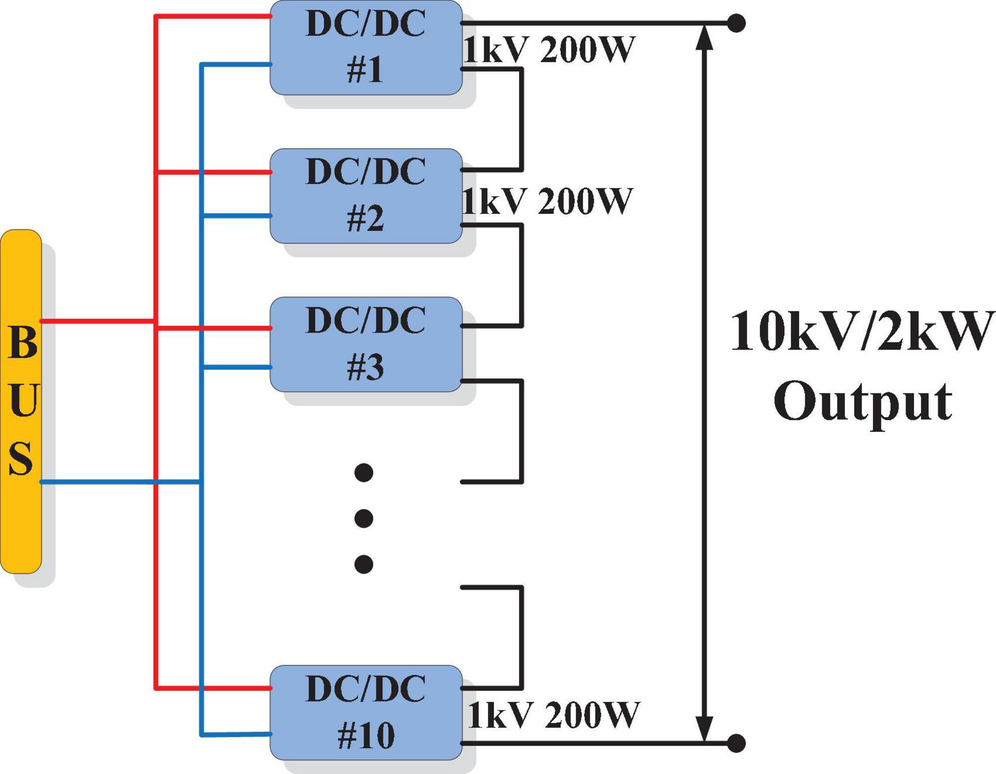
Figure 1. High-voltage converter topology for space welding.
The flexible combination of power supply modules for different space high-voltage applications is a well approach to solve the design problems of space high-voltage power supplies. Power supply modules can solve the problems in performance limitations of aerospace-grade devices in space high-voltage applications, and make it easier to carry out insulation protection. Therefore, space power module is very important in space high-voltage systems.
This paper proposes a space high-voltage power module with high boost ratio and a new improvement module to improve the efficiency.
Preliminary Design of Space High-Voltage Power Supply
Operation Mode Analysis
This paper proposes the preliminary design of the space high-voltage power module as shown in Figure 2A. The power inverter uses a full-bridge circuit, which can be used for high-power applications and improve the utilization of the transformer. The circuit employs a full-wave voltage doubler rectifier. Figures 2B,C depict the working state of this power supply.
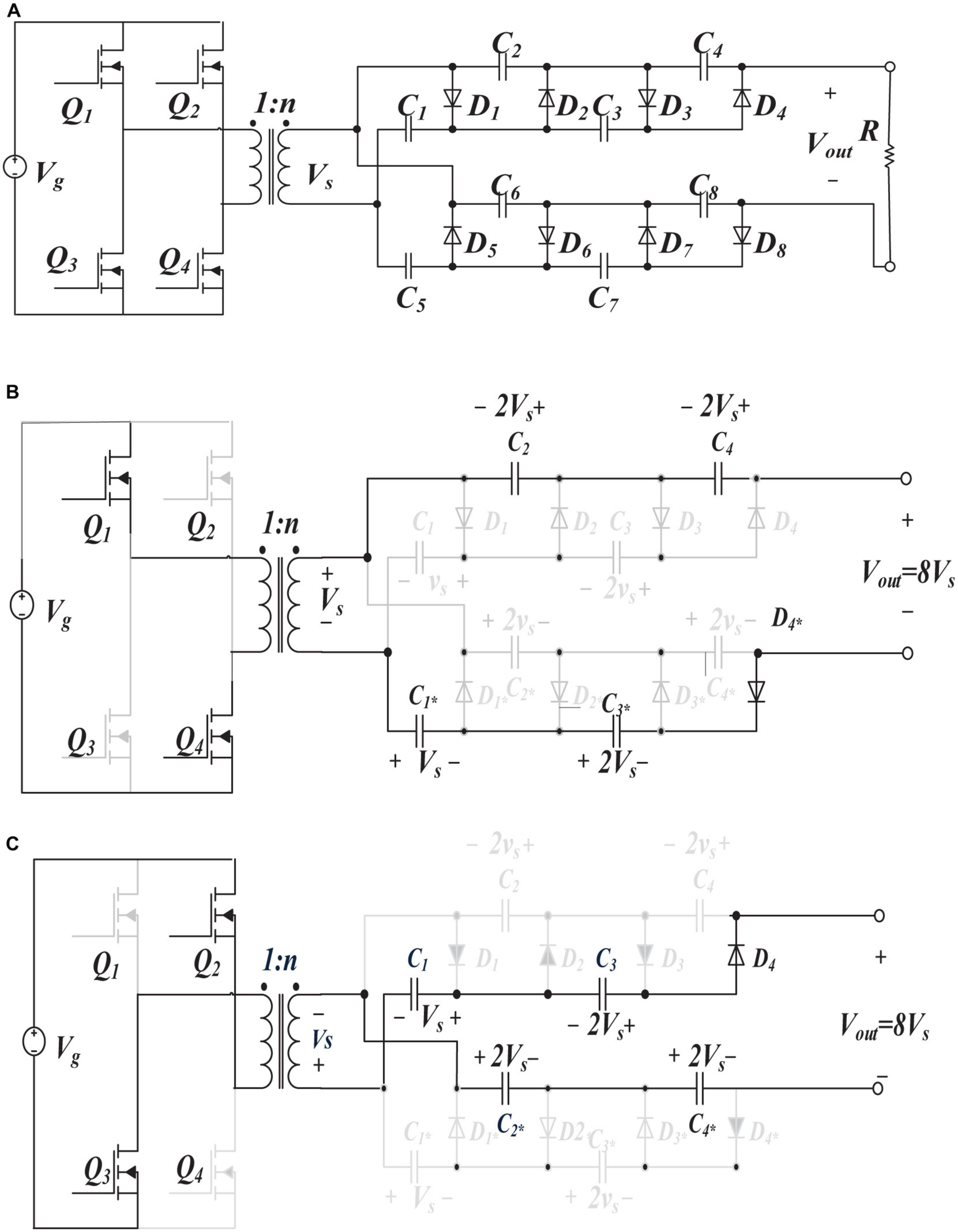
Figure 2. Preliminary design of space high-voltage power module topology and its operating modes. (A) Space high-voltage power module topology. (B) The first half-period. (C) The second half-period.
At the first half-period: Switches Q1 and Q4 are turned on, Q2 and Q3 are turned off, and the rectifier circuit outputs approximately 8 times the voltage of the secondary winding(Vin?) through the series of C1^*, C2, C3^*, C4 and the secondary winding.
At the second half-period: Switches Q2 and Q3 are turned on, Q1 and Q4 are turned off, and the rectifier circuit outputs approximately eight times the voltage of the secondary winding through the series of C1, C2^*, C3, C4^* and the secondary winding.
This design solves the problems of space high-voltage power supply, including high turn ratio transformers, secondary-side multi-windings in series with excessive stress and the power insulation. The maximum withstand voltage on the rectifier components (diodes and capacitors) of the rectifier is twice as the voltage of the transformer secondary windings. By reducing the turn ratio of the transformer and rectifying the output high-voltage through the voltage doubler rectifier, the voltage of the high-voltage transformer and the key rectifier components (diodes and capacitors) can be reduced, which improves the system reliability. Finally, the high-voltage power supply can be flexibly combined through IPOS to achieve voltage control and margin design.
Small Signal Analysis of Rectifier Circuit
The secondary side of the space high-voltage power module is full-wave eight-times voltage rectifier (as shown in Figure 2A). It is equivalent to the input-parallel-output-series connection of two half-wave four-times rectifier (shown in Figure 3). We establish a half-wave four-times voltage rectifier’s model and then derive it into a full-wave eight-times voltage rectifier.
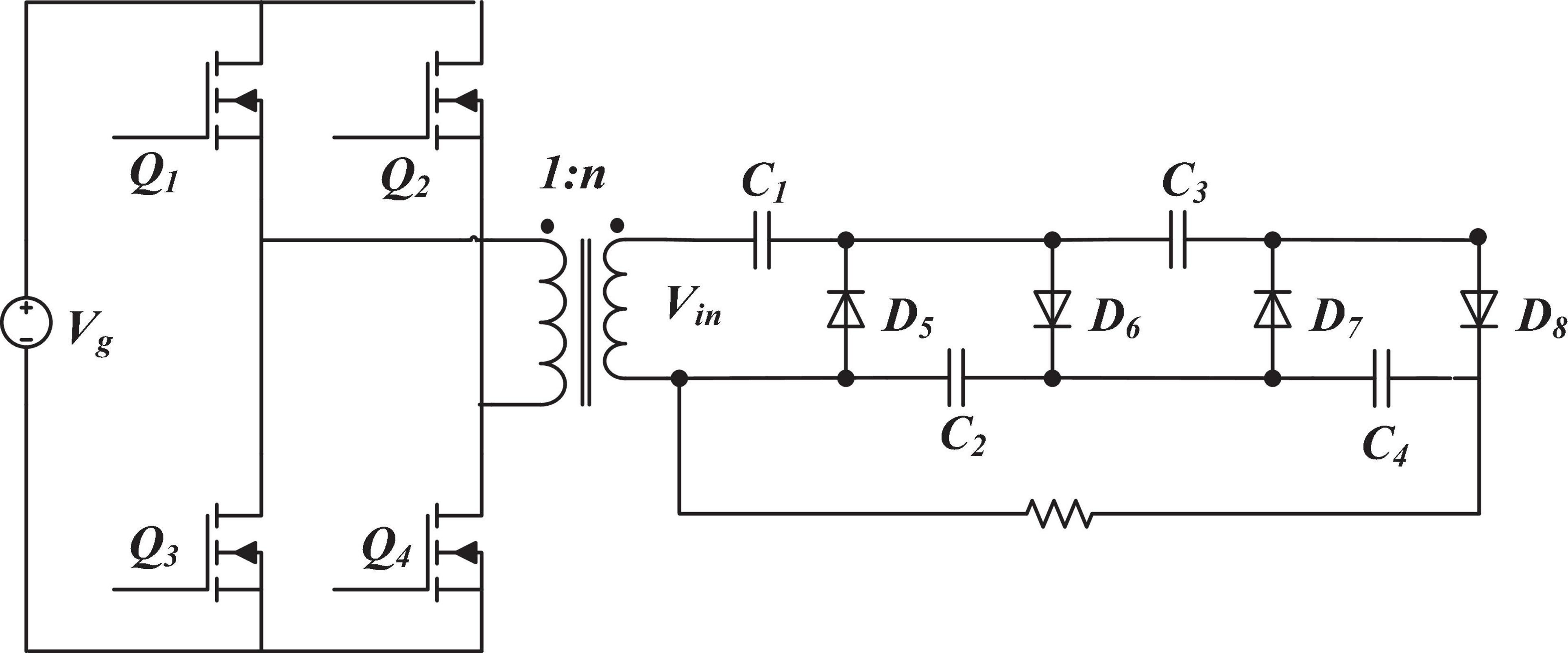
Figure 3. Half-wave four-times voltage rectifier.
For an ideal half-wave rectifier, the input voltage is shown in Figure 4. Assuming that the capacitance of the rectifier capacitor: Ci = C, (where i = 1,2…, n). The output voltage of half-wave four-times voltage rectifier is approximately equal to 4 Vin. We define four transfer functions of the two-port network:
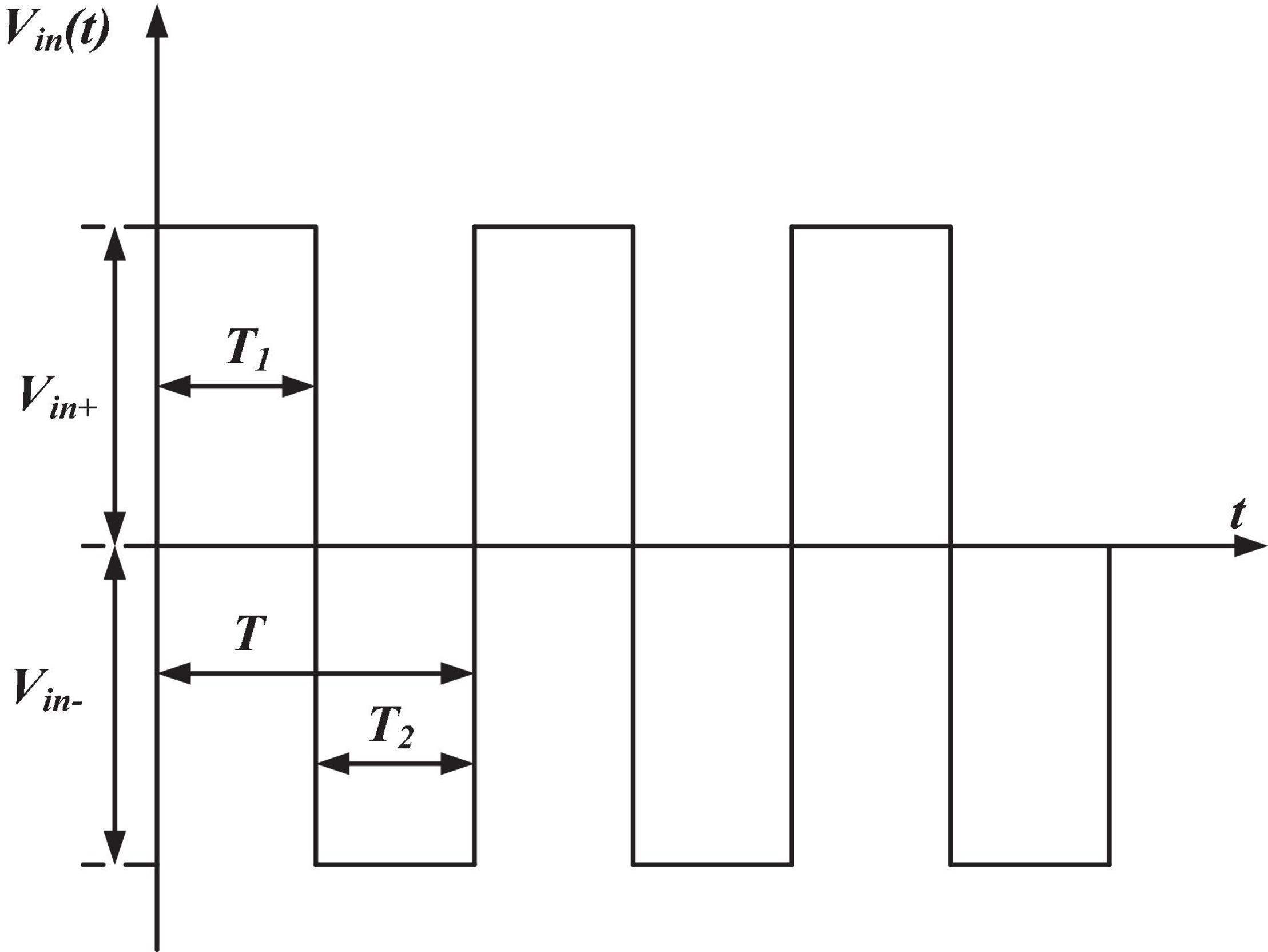
Figure 4. Input voltage waveforms of half-wave rectifiers.
The equivalent model of the small signal circuit can be obtained as shown in Figure 5, where G_v is the output voltage gain, Routis the output equivalent impedance, Yin is the input equivalent admittance and G_c is the reverse current gain.
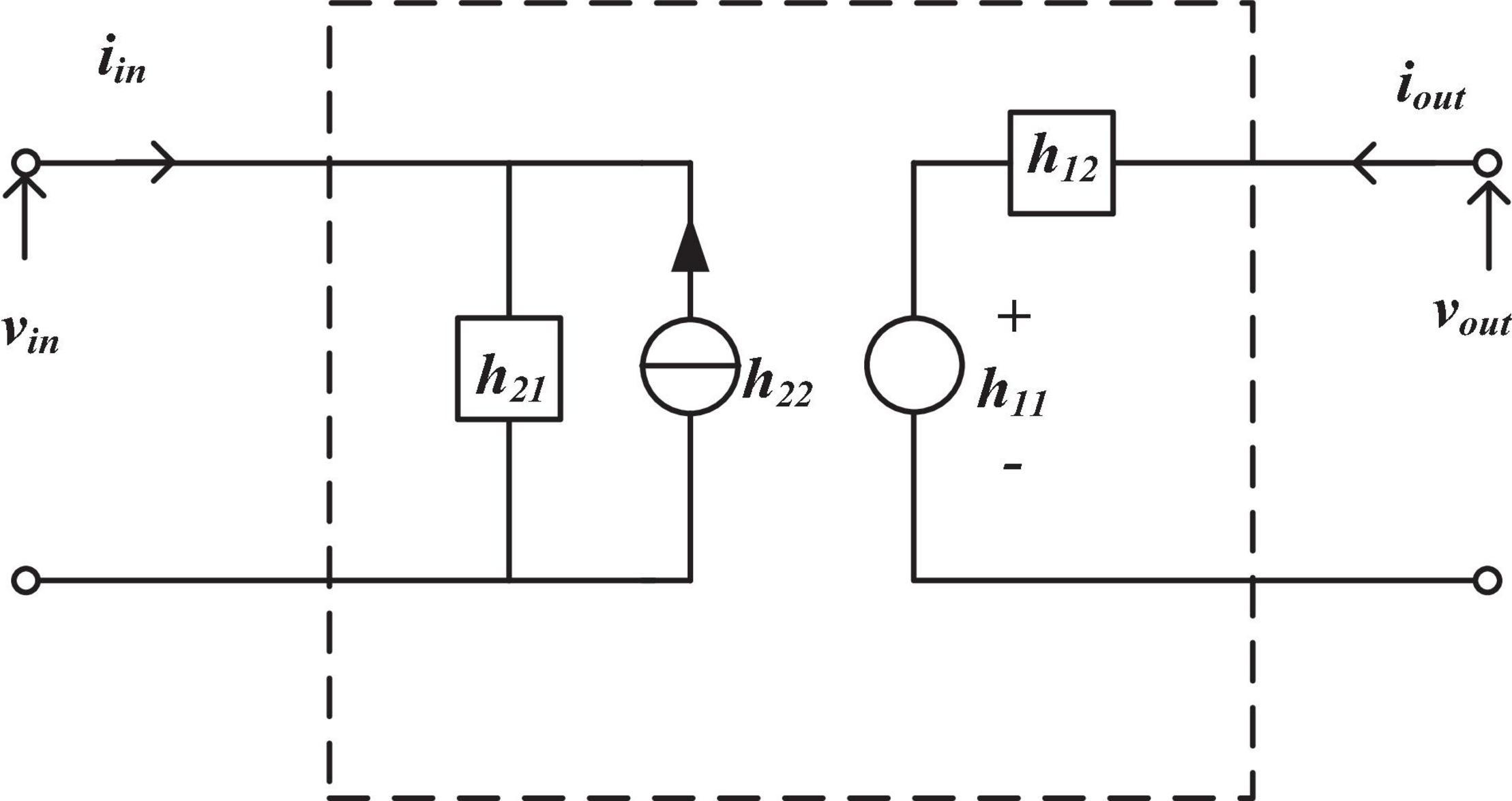
Figure 5. Small signal two-port equivalent circuits of rectifier.
As the input voltage is alternating between positive and negative, it can be regarded as discontinuous in time. This full-bridge half-wave rectifier is analyzed by the discrete system method. Firstly, by transforming the classical state space equations into discrete domain state space equations through z-transformation, the following state space equations are obtained:
where x is the state vector, u is the input vector and y is the output vector. Assuming that all rectifier units are ideal, that is, the on-resistance of the diode is 0, there is no on-voltage drop, the reverse cut-off voltage is large enough. The three vectors are expressed as follows:
By z-transformed on the discrete state space equations of Eq. (5), we get:
An equivalent transformation of Eq. (7) gives the relationship between the output matrix Y(z) and the input matrix U(z) as:
where the transfer function is:
Meanwhile, Eq. (9) is also the z-domain transfer function of Eqs (1–4). For z = ejwt, we can calculate the amplitude-frequency characteristic |hij(jwt)| and the phase frequency characteristic ∠|hij(jwt)| of the four transfer functions.
For a half-wave four-times rectifier, the four matrices A–D are all 2 × 2 arrays and the system is a two-input, two-output system. By calculating the coefficients of the four matrices, a complete transfer function of a half-wave voltage doubler rectifier can be obtained, and by connecting two identical systems with the inputs in parallel and outputs in series, an expression for a full-wave eight-times rectifier can be obtained. Then we create a complete small signal model, where the equivalent circuit diagrams for (kT)∼(kT + T1)and (kT + T1)∼[(k + 1)T] periods are shown in Figure 6.
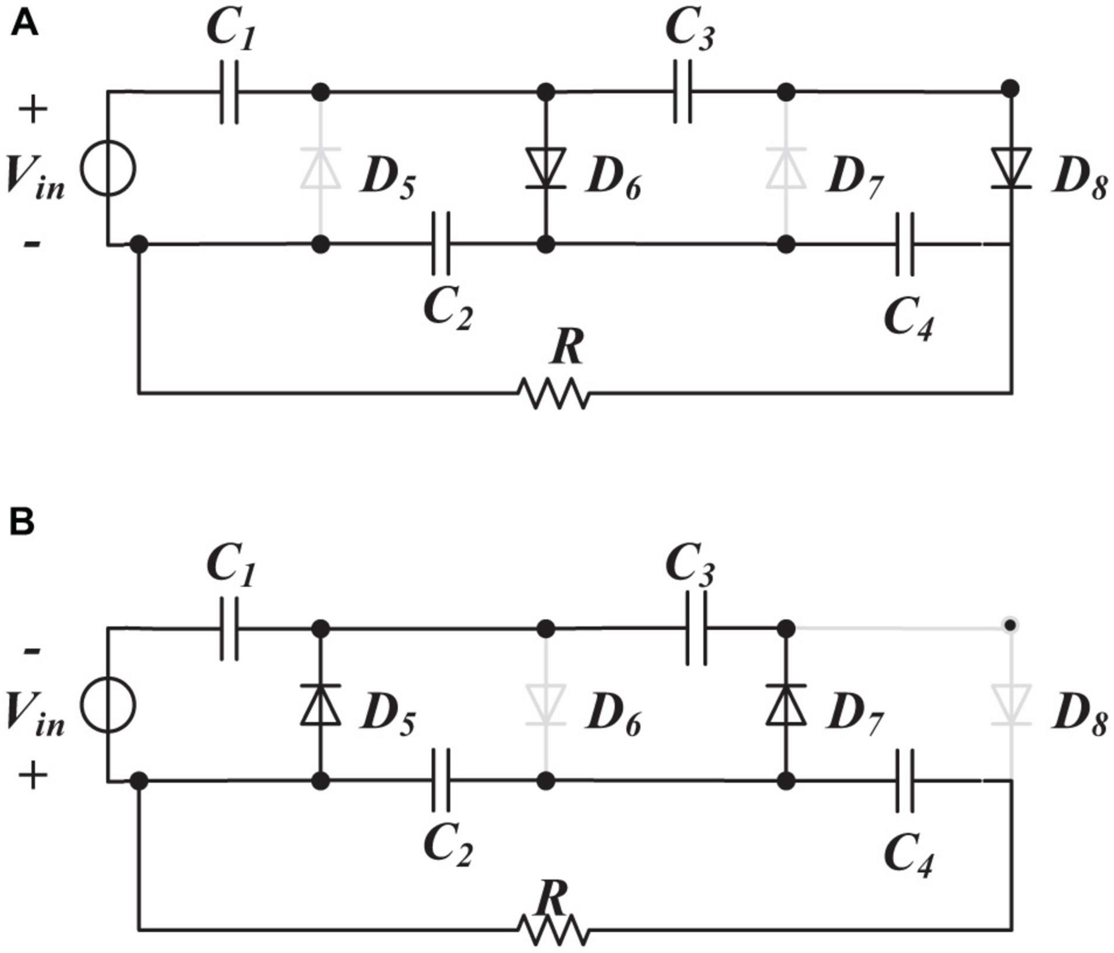
Figure 6. Equivalent circuit for (k+1) cycle circuit operation. (A) (kT)∼(kT + T1). (B) (kT + T1)∼[(k + 1)T].
where C2 and C4 act as voltage output capacitors and provide a doubling output to load R. At the beginning of the two periods, it is equivalent to two capacitors C2 and C4 in parallel with resistance R/2, respectively, and the capacitor is discharged through the RC circuit.
Starting from kT, the polarity of the input voltage is in Figure 4. We can derive the output voltages of capacitors C2, and C4. Since it is assumed that diodes are ideal in the topology of this circuit, capacitors C1 and C2, capacitors C3 and C4 are instantaneously connected in parallel, respectively. According to Kirchhoff’s voltage law (KVL) and conservation principles of capacitor charge, it can be deduced that:
Adding small signal perturbations [we consider v2(t) = v1(t), v4(t) = v3(t)] to the steady state quantities, the expressions (10) (11) are organized as:
From k+T to (kT+T1)–, the voltage drop of capacitors C2 and C4 equals to the integral of the equivalent resistive current from 0 to T1 multiply by the reciprocal of the equivalent supply capacitance.
Starting from k(T + T1), the polarity of the input voltage is in Figure 4. We can derive the two output capacitor voltages. Since the diode is assumed as an ideal device, at this moment the capacitors C2 and C3 are instantaneously connected in parallel, and their voltages are equal at both ends according to KVL and conservation of capacitive charge.
By adding small signal perturbations [we consider v2(t) = v3(t)] to the steady state quantities, the expressions (16) (17) are organized as:
From to [((k + 1)T)−], the voltage drop of capacitors C2 and C4 equals to the integral of the equivalent resistive current from 0 to T2 multiply by the reciprocal of the equivalent supply capacitance.
From the Eqs (21) and (22), we can derive that at the end of T2, the voltage across capacitors C2 and C4 are calculated as:
Then the voltage drop of the main output capacitor from to (k + 1)T− has been calculated. Bringing Eqs (22) and (23) into Eqs (12) and (13), we can derive an expression for the voltages of capacitors C2 and C4 in the first switching mode.
Separating the small signal variables of the entire circuit from the above equation, a set of equations can be listed as follows:
Similarly, the expressions of other transfer function parameter matrices can be derived.
The system transfer function is calculated by MATLAB, there is an output impedance zero pole diagram for a full-wave eight-times rectifier as shown in Figure 7A, an output impedance bode diagram as shown in Figure 7B, a voltage gain zero pole diagram for a full-wave eight-times rectifier as shown in Figure 7C and a voltage gain bode diagram as shown in Figure 7D. For discrete systems, the system is stable because the poles of the voltage gain transfer function and the impedance gain transfer function are all in the unit circle in the z-plane.
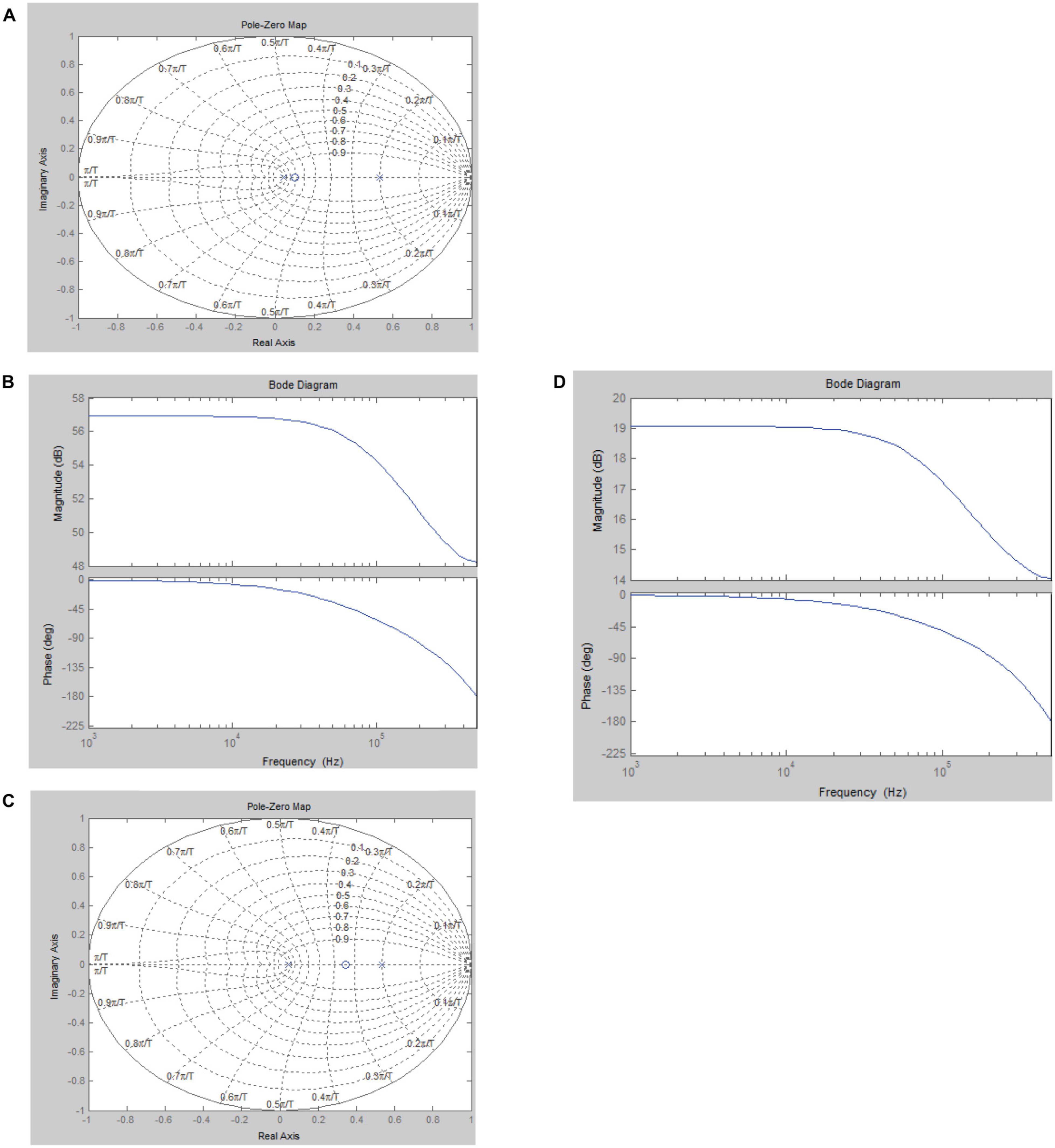
Figure 7. Small signal model simulation diagram. (A) Zero pole diagram of output impedance. (B) Bode diagram of output impedance. (C) Zero pole diagram of voltage gain. (D) Bode diagram of voltage gain.
Steady-State and Transient Charging Processes of Rectifier Capacitors
In Figure 2A, assuming that the voltage on the transformer secondary side is Vs, when the transformer is working in a steady state, the positive half cycle can be deduced as:
In this power module, the rectifier capacitor can be charged and discharged in half a working cycle (switching cycle). According to the law of conservation of electric charge and KVL, in the half-switching cycle at the beginning of the circuit’s operation, we can derive that:
By using the same type of high-voltage diode in the circuit, the forward voltage drop VD of each diode is equal:
Similarly, for the other part of the circuit, there is:
By bringing Eqs (28) and (29) into Eq. (26), the following output voltages can be obtained for the full-wave eight-times rectifier circuit (Figure 2A):
The forward voltage drop VD of the rectifier diode is negligible relative to the transformer secondary side voltage VS, so the output voltage in Figure 2A is approximately eight times as VS. Extending this to a full-wave 2n voltage doubler rectifier circuit, it can be seen that only capacitors C1 and C1^* have a voltage of | VS| − VD, while capacitors Cn and Cn^* (n > 1) both have twice the voltage of | VS| − VD.
However, the above discussion only applies to the steady-state capacitors in the voltage doubler rectifier, while the transient charging circuit of the capacitors is shown in Figure 8.
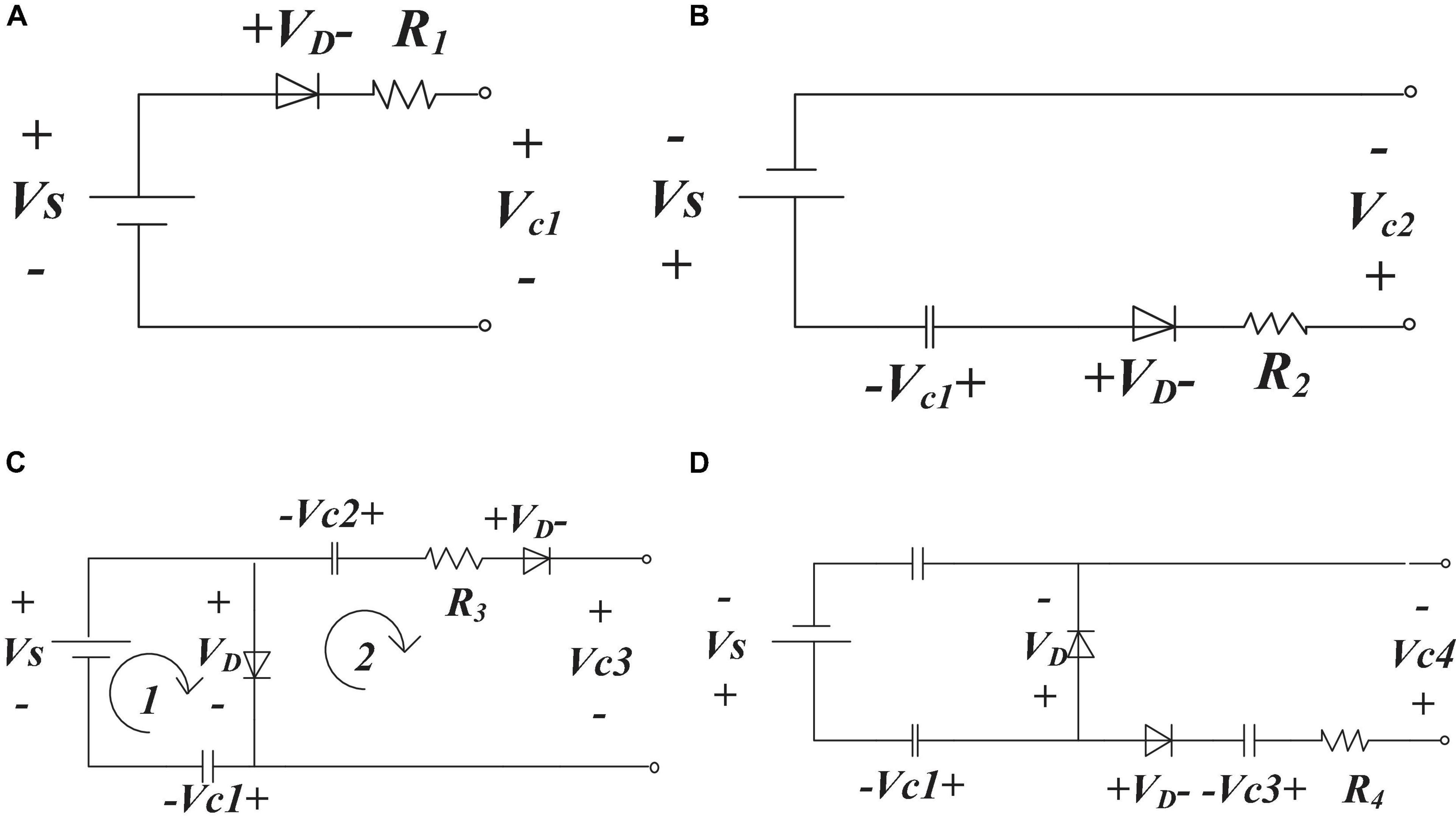
Figure 8. Capacitor charging circuit. (A) Capacitor C1 charging, (B) capacitor C2 charging, (C) capacitor C3 charging, and (D) capacitor C4 charging.
The maximum voltage across capacitance C1 is:
The charging voltage of the capacitor at t is (where R is the equivalent resistance of the forward charging path):
We calculate that when t = αRC, where α = 3∼5, VC1 ≥ 0.96E, the microscopic capacitance C1 voltage drop is slightly less than E. When the capacitor is discharged:
Also after t = αRC, where α = 3∼5, VC1’ ≤ 0.04VC1. The voltage at one charge and discharge of capacitor C1 is:
When the first switching cycle ends, C1 transfers its own power to C2. The voltage of C2 is:
At the beginning of the first half of the next cycle, C1 is charged to VC1 = E × (), then, according to KVL, in loop 2 (Figure 8C), since the diodes have the same forward voltage drop, capacitor C2 charges to capacitor C3:
At the start of the second half of the cycle, C3 charges to capacitor C4, in the same way as above:
According to KVL:
This is the end of the second switching cycle, VC2″ > VC2, and the cycle continues until each capacitor is charged to a value close to the theoretical value of Eq. (29), then it achieves the steady state.
During the first half of each cycle in steady state, capacitors C1 and C3 are charged to their theoretical values, C2 and C4 supplies the load, C1 and the secondary side winding charges C2 and C3 charges C4 during the second half of the cycle. The C1*, C2*, C3*, and C4* transient and steady-state operating mode in the circuit are reversed, so that we achieve a stable DC output over the entire switching cycle. And the theoretical waveforms for capacitors transient charging are shown in Figure 9A.
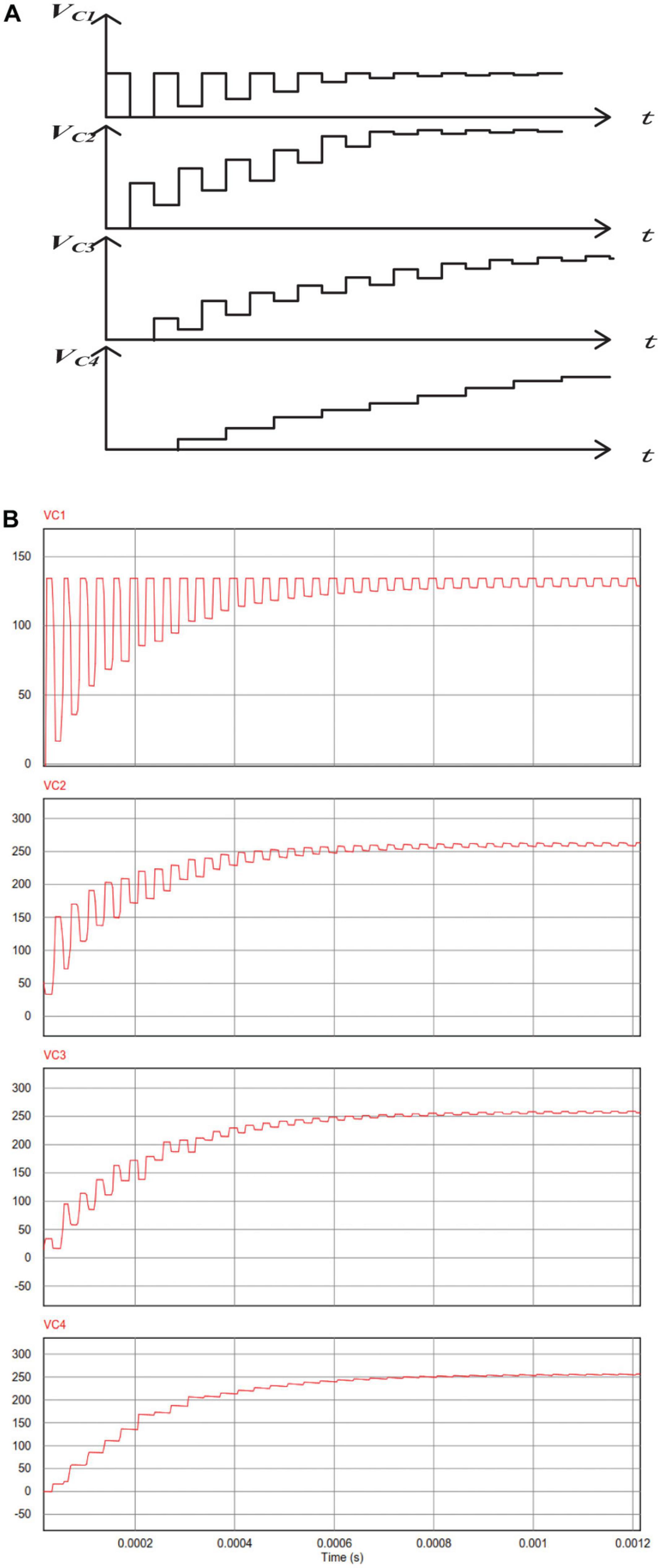
Figure 9. Waveform for capacitors transient charging. (A) Theoretical waveforms for capacitors transient charging. (B) Simulation waveforms for capacitors transient charging.
We use PSIM, a circuit simulation software, to simulate the capacitor charging of the full-wave voltage doubler rectifier. The simulation result is shown in Figure 9B, which verifies the capacitor transient charging analysis. It also verifies that a stable high-voltage DC output can be achieved when the full-wave voltage doubler rectifier is in steady-state operation.
Experimental Verification
We design a power module as shown in Figure 2A, which the input voltage is 100 V, the output voltage is 1,000 V, the switching frequency is 50 kHz, and the maximum output power is greater than 200 W. The waveforms of the corresponding rectifier collected through experiments are shown in Figure 10. Figure 11 is the power module prototype.
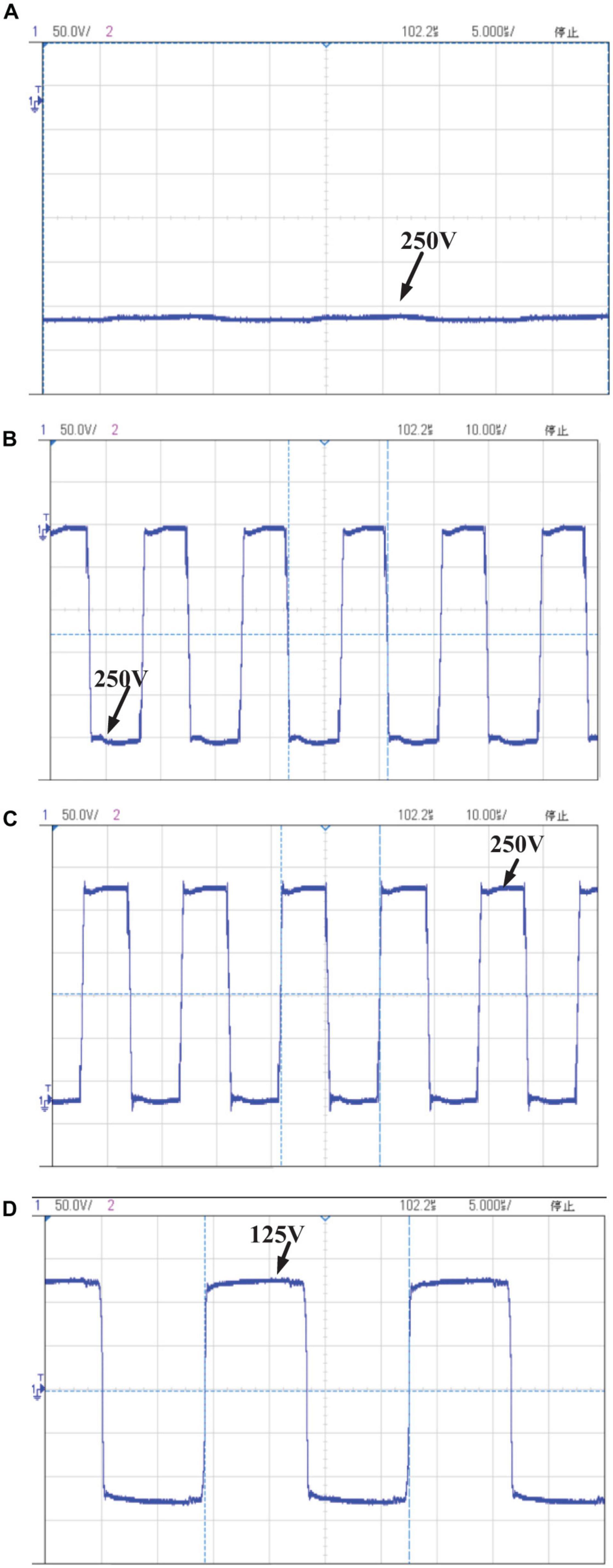
Figure 10. Experimental waveform of each device when the circuit output is 1,000 V of Figure 2A. (A) Voltage waveform of capacitor C2 (Figure 4) at 1,000 V output. (B) Voltage waveform of diode D1 (Figure 4) at 1,000 V output. (C) Voltage waveform of diode D2 (Figure 4) at 1,000 V output. (D) Voltage waveform of transformer secondary windings (Figure 4) at 1,000 V output.
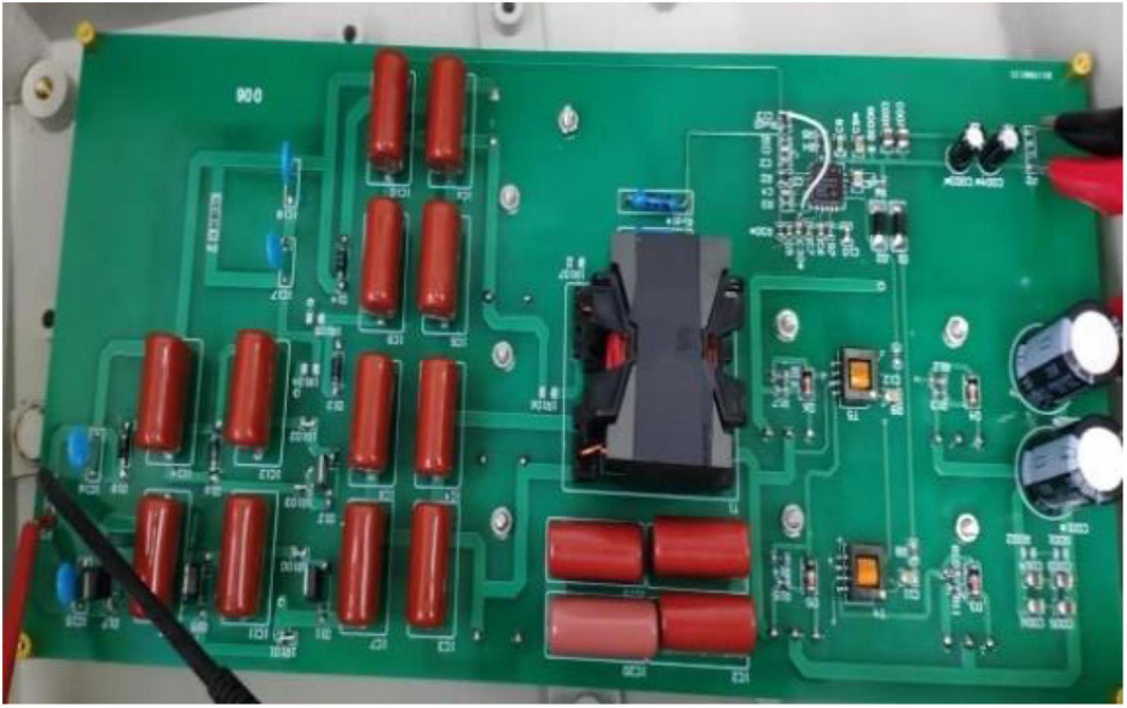
Figure 11. High-voltage power module prototype.
After experimental verification, the preliminary designed power module can reduce the voltage stress of key components. When the output is 1,000 V, the withstand voltage of the rectifier device is only 250 V, and the secondary windings’ voltage of the transformer is only 125 V.
The load we used in the experiment is linear resistance. However, according to the efficiency curve, it can be seen that the power module’s efficiency is slightly lower than the simulation, and the efficiency needs to improve. By calculating and observing the waveform of the switching device of the inverter in the oscilloscope, the circuit loss is concentrated on the on and off losses of the switch and other power devices. Then, we propose an improved power module.
Improved Design High-Voltage Power Supply
In the previous section, the proposed space high-voltage power supply module can reduce the voltage of key components, which improves the reliability of the system to a certain extent. Inspired by paper (Yao et al., 2011; Karimi et al., 2014), we propose soft-switching to improve the efficiency of this power module.
Circuit Improvement Design
The improved inverter is a series resonant phase-shifted full-bridge circuit. The circuit topology is shown in Figure 12A. DCDC phase-shift switching technology is used to reduce switching losses. If the voltage Vds is zero before the switch is turned on or the current is zero when it is turned on, then the switch conduct loss is zero, then, Zero Voltage Switch (ZVS) and Zero Current Switch (ZCS) are realized. The switch state diagram is shown in Figure 12B.
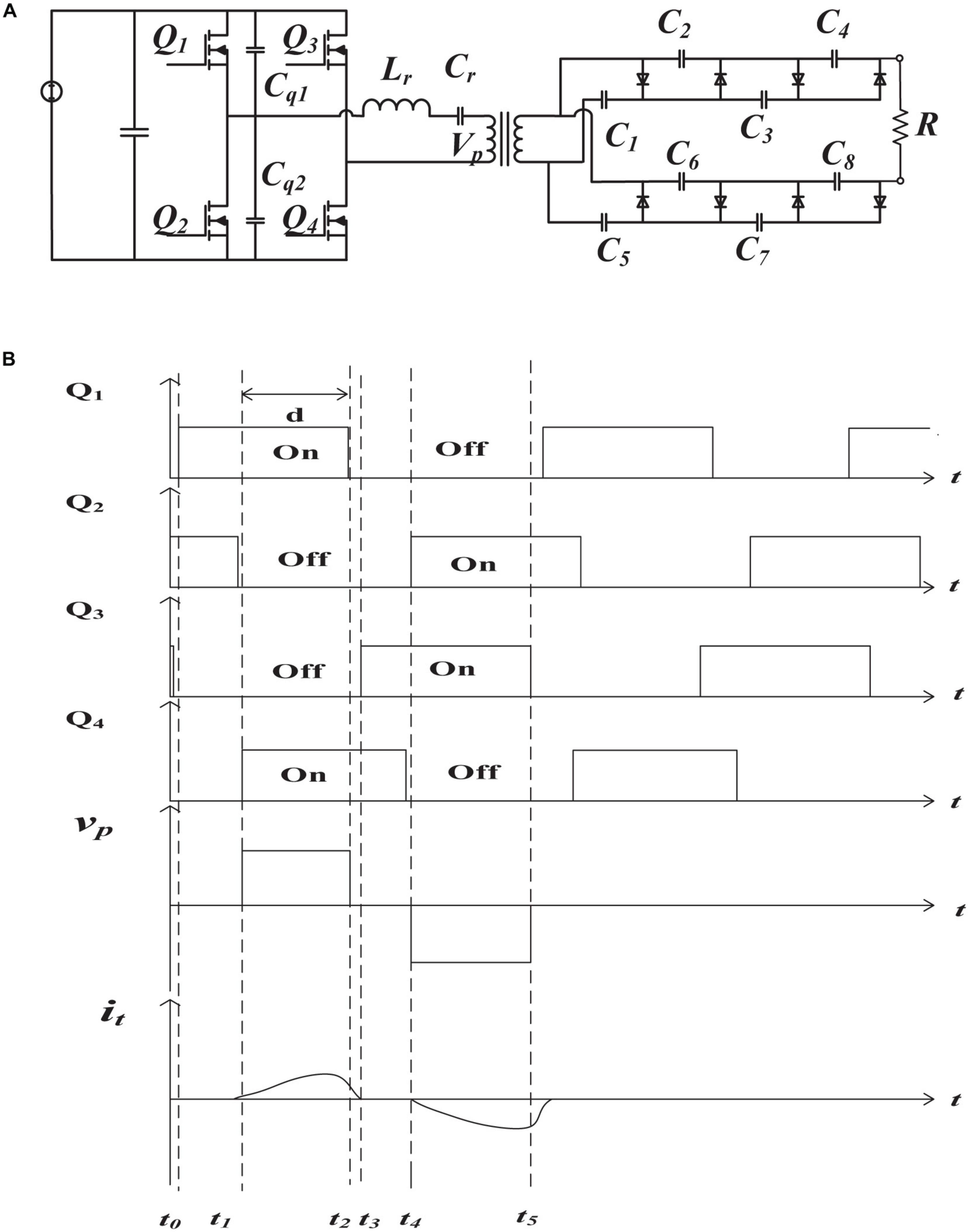
Figure 12. Improved space high-voltage power module. (A) Improved circuit. (B) Switch state and transformer waveform.
[t0 − t1]: Q1 and Q2 are turned on at the same time, the voltage and current on the transformer are both zero, the output terminal supplied power to the load, and the switch Q2 is turned off under ZCS conditions;
[t1 − t2]: At the beginning of this moment, the switch Q4 is turned on under the condition of ZCS, at this time the current of the resonance circuit start to increase, and the rectifier capacitor is charged;
[t2 − t3]: At the beginning of this period, switch Q1 is turned off, capacitor Cq1 is charged, capacitor Cq2 is discharged, and the circuit continues to flow through Lr. When capacitor Cq2 is discharged to 0, this period ends. The primary side circuit current is gradually decreasing to supply the load;
[t3 − t4]: The voltage across the parallel absorption capacitor Cq2 of switch Q3 drops to zero, and the current continues to flow through the body diode in Q3. Q3 is turned on under the condition of ZVS. The Vp drops to zero;
[t4 − t5]: Q2 is turned on under the condition of ZCS, the primary side circuit conducted reversely, charges to the secondary capacitor, Q3 is turned off, and this period ends.
Circuit Performance Analysis
As shown in Figure 12A, the primary voltage of the transformer is Vp and the number of winding turns are Np; the secondary voltage of the transformer is Vs and the number of winding turns are Ns; the input voltage of the circuit is Vin and the output voltage is Vo; the steady-state duty cycle is d, where d = . When Q1 and Q4 are turned on and Q2 and Q3 are turned off, there is:
According KVL:
According to the inductance volt-second balance:
Combine (45) (46) (47):
Solve the output voltage Vo as:
According to the conservation of input and output energy of the power supply, the input inductor current IL is derived as:
where R is the load resistance and η is the efficiency of the power supply.
Circuit Verification
The simulation circuit is depicted in Figure 12A. The simulation results are shown in Figures 13A,B, and the efficiency comparison is depicted in Figure 13C. The simulation parameters are shown in Table 1.
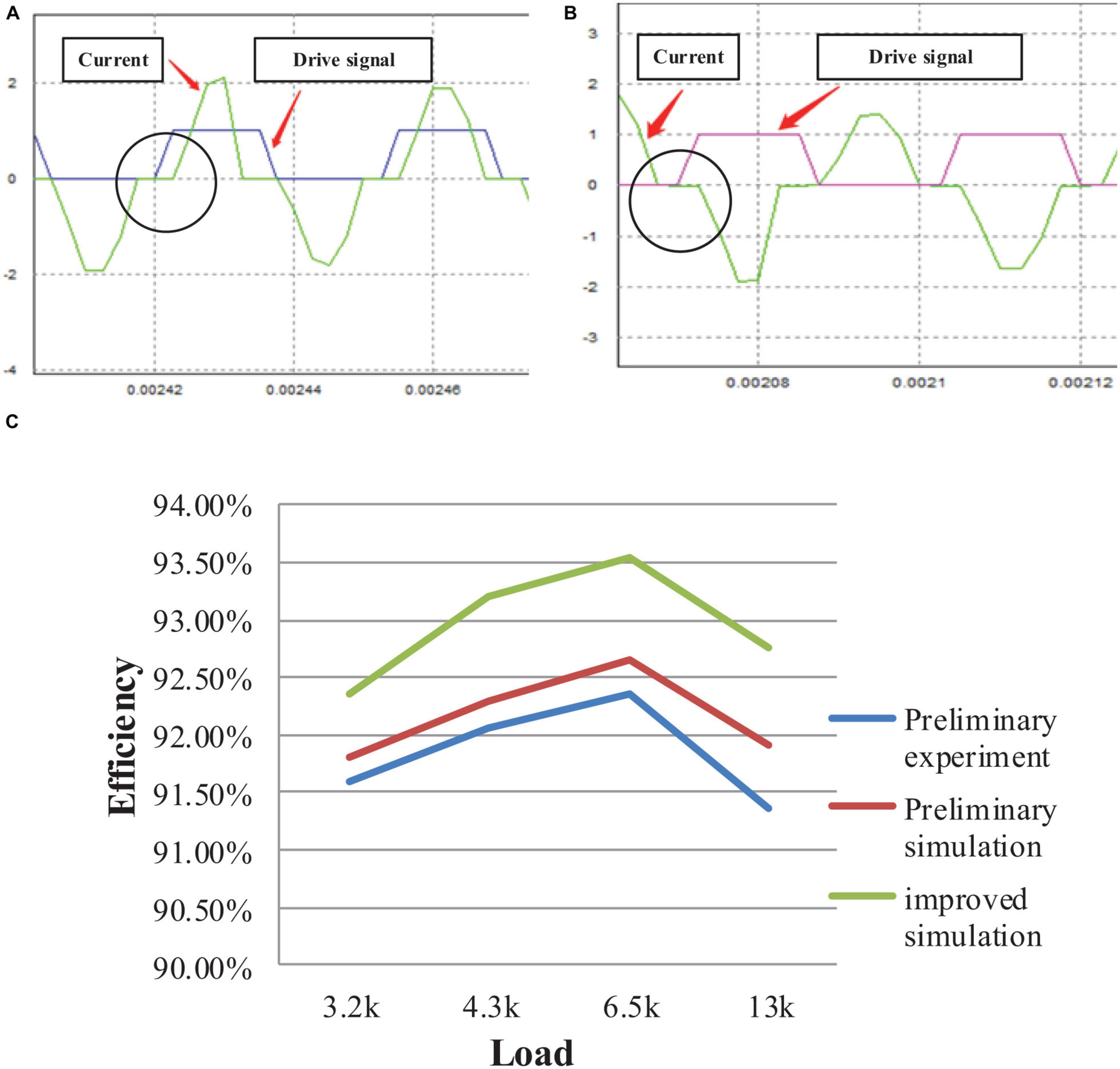
Figure 13. Efficiency comparison. (A) Simulation Q2. (B) Simulation Q3. (C) Efficiency comparison.
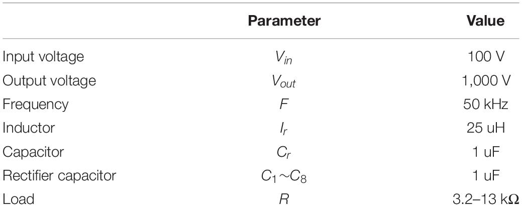
Table 1. Simulation parameters.
According to the simulation results, the switches Q2 and Q3 in the improved circuit can achieve ZCS conduction, and the simulation efficiency is higher than the efficiency obtained from the preliminary experiment. Therefore, the improved topology is suitable for space high-voltage power modules.
Electric Field Simulation
Space high-voltage applications are important in aerospace, so attention must be paid to the space environment adaptability and reliability of high-voltage space electronics.
Base on the phenomenon of space low-pressure discharge, the space high-voltage power module is designed with high reliability (especially the placement of components), and the proposed power module is verified by electric field simulation (Maxwell of Ansoft). Figure 14A shows the three-dimensional electric field distribution of the high-voltage part of the power module (rectifier), and Figure 14B shows the contour electric field distribution of the high-voltage part of the power module.
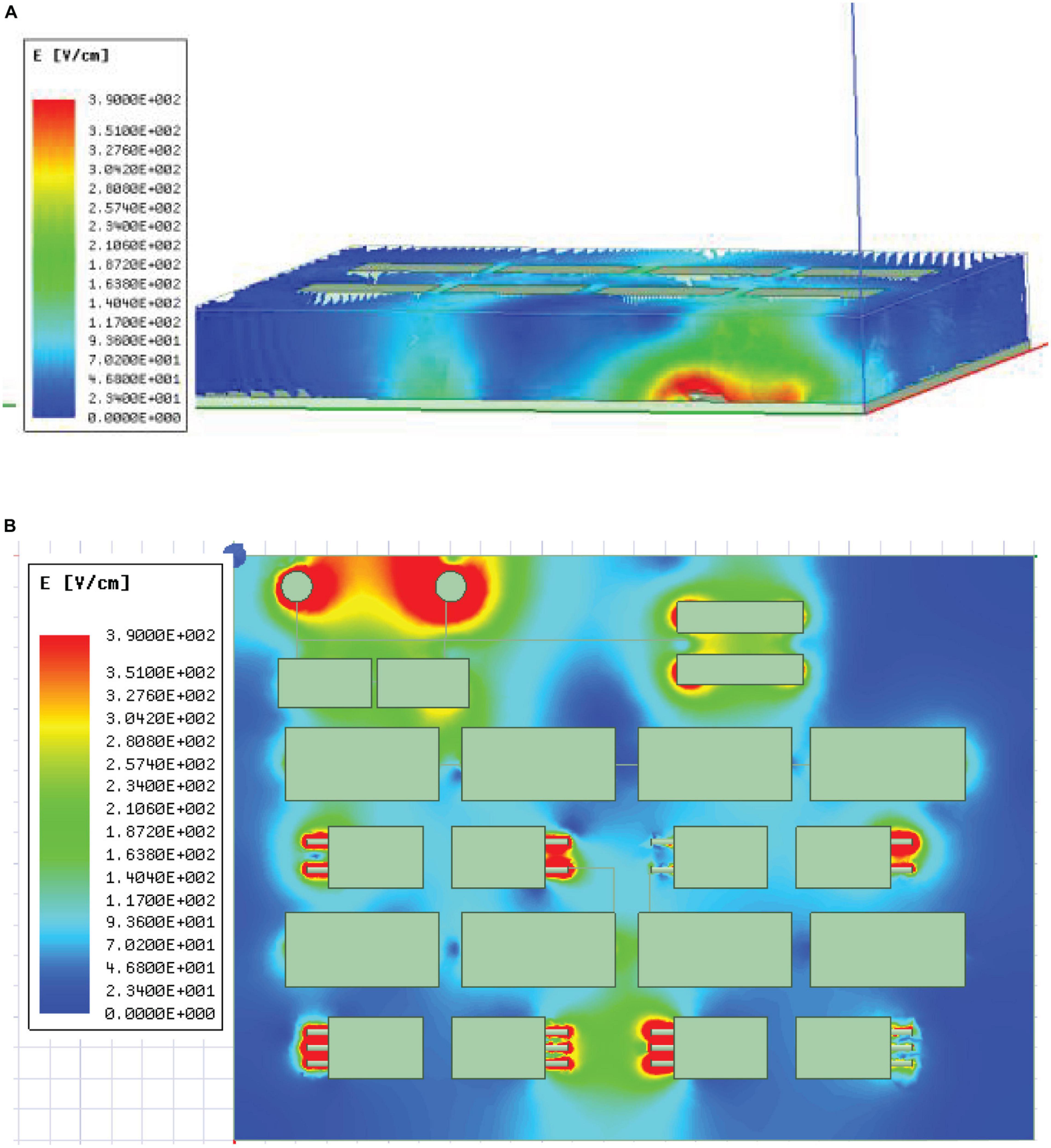
Figure 14. Electric field distribution. (A) Three-dimensional electric field distribution. (B) The contour electric field distribution.
It can be seen from the Figure 14 that the high electric field of the Printed Circuit Board (PCB) is concentrated in the red area of the figures. With this layout, the maximum electric field strength is 390 V/cm. The design of the space high-voltage power supply module meet the standards in the ECSS-E-HB-20-05A (Ecss, 2012).
Conclusion
Based on my own work (Wen-jie et al., 2020) in 2020 2nd International Conference on Smart Power & Internet Energy Systems (SPIES), this paper focuses on the detailed theoretical design of high-voltage power module. Through theoretical analysis, simulation and experimental verification, we believe that the high-voltage power supply has high reliability.
This paper analyses the application scenarios of space high-voltage power supply systems and the advantages of power supply modules under the constraints of space applications. We design a 200 W space high-voltage power supply module with 100 V input and 1,000 V output. We carry out a stability analysis of the circuit by a small signal equivalent model and a capacitor charging model. This power module reduces the voltage stress of key components in the rectifier.
Then we optimize the power module: an improved design base on a phase-shifted full-bridge series resonant circuit. In addition to reducing the voltage stress on key components such as rectifier and high-voltage transformer, the improved power module achieves soft-switching, which greatly reduces the high-frequency switching losses of power switching devices in inverter. The improved high-voltage power module is more efficient than the preliminary power module. Then, the improved solution is validated by simulation.
We carry out the electric field on the high-voltage PCB section (rectifier) of the power supply module. This allows us to focus on the insulation protection areas on the PCB in our designs.
Finally, we believe that space high-voltage power supply systems are in a phase of rapid development. The circuit topology, electronic components and insulation protection are the focus of the development of space high-voltage power supplies. High-voltage power supply modules with a stable output voltage, a wide range of adjustable output power and the high reliability will be more flexible to meet the requirements of most space high-voltage applications.
Data Availability Statement
The original contributions presented in the study are included in the article/supplementary material, further inquiries can be directed to the corresponding author.
Author Contributions
WZ contributed to the designs, experiments, and completes most part of the manuscript. YJ completes most part of the simulations. JW helped in most of the experiments. YH performed as faculty adviser and manuscript reviser. YZ and CW performed as faculty adviser. JA performed as faculty adviser and helped in most simulation. All authors contributed to the article and approved the submitted version.
Conflict of Interest
JW and CW were employed by the company China Aerospace Science and Technology Corporation.
The remaining authors declare that the research was conducted in the absence of any commercial or financial relationships that could be construed as a potential conflict of interest.
Acknowledgments
This manuscript has previously been published as a conference manuscript at the 2020 2nd International Conference on Smart Power & Internet Energy Systems (https://ieeexplore.ieee.org/document/9243142). First of all, we thank the 2020 2nd International Conference on Smart Power & Internet Energy Systems (SPIES), Bangkok, Thailand for recommending our manuscript to the Frontiers in Energy Research, section Smart Grids. This work was carried out by the National Space Science Center, CAS and Beijing Spacecraft, CAST. Thanks are due to JW for assistance with the experiments and to YH and CW for valuable discussion.
References
Bekemans, M., Bronchart, F., Scalais, T., and Franke, A. (2019). “Configurable high voltage power supply for full electric propulsion spacecraft,” in Proceedings of the 2019 European Space Power Conference (ESPC), (Juan-les-Pins: IEEE), 1–5. doi: 10.1109/ESPC.2019.8931988
Ecss (2012). ECSS-E-HB-20-05A Space Engineering High Voltage Engineering And Design Handbook. Noordwijk: ECSS.
Forrisi, F., Mache, E., Mallmann, A., and Blaser, M. (2019). “Compact low cost high voltage power supply for space applications,” in Proceedings of the 2019 European Space Power Conference (ESPC), (Juan-les-Pins: IEEE), 1–5. doi: 10.1109/ESPC.2019.8931982
Fu, M., Zhang, D., and Li, T. (2017). New electrical power supply system for all-electric propulsion spacecraft. IEEE Trans. Aerosp. Electron. Syst. 53, 2157–2166. doi: 10.1109/TAES.2017.2683638
Karimi, R., Adib, E., and Farzanehfard, H. (2014). Resonance base zero-voltage zero-current switching full bridge converter. IET Power Electron. 7, 1685–1690. doi: 10.1049/iet-pel.2013.0301
Lord, P. W., Tilley, S., and Baldwin, J. (2020). “Commercial solar electric propulsion: a roadmap for exploration,” in Proceedings of the 2020 IEEE Aerospace Conference, (Big Sky, MT: IEEE), 1–16. doi: 10.1109/AERO47225.2020.9172330
Novac, B. M., Smith, I. R., Senior, P., Parker, M., and Louverdis, G. (2010). “High-voltage pulsed-power sources for high-energy experimentation,” in Proceedings of the 2010 IEEE International Power Modulator and High Voltage Conference, (Atlanta, GA: IEEE), 345–348.
Reese, B., Hearn, C., and Lostetter, A. (2013). “Silicon carbide base anode supply module array for hall effect thrusters,” in Proceedings of the 2013 IEEE Aerospace Conference, (Big Sky, MT: IEEE), 1–8. doi: 10.1109/AERO.2013.6496863
Wang, L., Zhang, D., Duan, J., and Li, J. (2018). “Design and research of high voltage power conversion system for space solar power station,” in Proceedings of the 2018 IEEE International Power Electronics and Application Conference and Exposition (PEAC), (Shenzhen: IEEE), 1–5. doi: 10.1109/PEAC.2018.8590543
Wen-jie, Z., Cheng-an, W., Yi-fei, G., Guo-shuai, Z., Yan, Z., Yong-gang, C., et al. (2020). “Space high voltage power module design,” in Proceedings of the 2020 2nd International Conference on Smart Power and Internet Energy Systems (SPIES), (Bangkok: IEEE), 1–6. doi: 10.1109/SPIES48661.2020.9243142
Xin-bin, H., and Li, W. (2015). Present Situation and Prospect of SPS Technology Development. Beijing: Aerospace China, 12–15.
Yao, C., Ruan, X., Wang, X., and Tse, C. K. (2011). Isolated buck–boost DC/DC converters suitable for wide input-voltage range. IEEE Trans. Power Electron. 26, 2599–2613. doi: 10.1109/tpel.2011.2112672
Zaitsev, R. V., Kirichenko, M. V., Minakova, K. A., Khrypunov, G. S., zdov, A. N., Khrypunova, I. V., et al. (2019). “DC-DC converter for high-voltage power take-off system of solar station,” in Proceedings of the 2019 IEEE 2nd Ukraine Conference on Electrical and Computer Engineering (UKRCON), (Lviv: IEEE), 1–6. doi: 10.1109/UKRCON.2019.8879860
Keywords: space high-voltage power supply, high-efficiency power conversion, environmental adaptability, full-wave voltage doubler rectifier, electric field simulation
Citation: Zhao W, Jiang Y, Wu J, Huang Y, Zhu Y, An J and Wan C-a (2021) Space High-Voltage Power Module. Front. Energy Res. 9:642920. doi: 10.3389/fenrg.2021.642920
Received: 17 December 2020; Accepted: 01 March 2021;
Published: 01 April 2021.
Edited by:
Farhad Rachidi, École Polytechnique Fédérale de Lausanne, SwitzerlandReviewed by:
Md. Abdur Razzak, Independent University, Dhaka, BangladeshSudhakar Natarajan, VIT University, India
Copyright © 2021 Zhao, Jiang, Wu, Huang, Zhu, An and Wan. This is an open-access article distributed under the terms of the Creative Commons Attribution License (CC BY). The use, distribution or reproduction in other forums is permitted, provided the original author(s) and the copyright owner(s) are credited and that the original publication in this journal is cited, in accordance with accepted academic practice. No use, distribution or reproduction is permitted which does not comply with these terms.
*Correspondence: Wenjie Zhao, endqb2sxMjNAMTI2LmNvbQ==