 Mohammad Ali Akhavan Kazemi1
 Frédéric Sauvage
- 1Laboratoire de Réactivité et Chimie des Solides (LRCS), UMR CNRS 7314—Institut de Chimie de Picardie FR 3085, Université de Picardie Jules Verne, Amiens, France
- 2Plateforme de Microscopie Électronique, Université de Picardie Jules Verne, HUB de L’Energie, Amiens, France
The time and annealing temperature for the film crystallization in perovskite solar cells (PSCs) is critical and is at the stake of device optimization. It governs the crystallization process, the film’s morphorlogy and texture and the level of non-radiative defects, which in whole control the power conversion efficiency (PCE). However, deciphering each of these parameters in the device cell characteristics remains not totally clear. In this work, we led a holistic study considering temperature and time for the MAPbI3 crystallization as a free parameter to study how the latter is impacting on the film’s characteristics and how the device figure of merit is affected. The results suggest that the crystallinity level of the grains plays an important role in the photo-current value whereas the morphology and PbI2 impurities resulting from the onset of thermal decomposition of MAPbI3 penalizes the cell photovoltage and the fill factor values. Based on this study, it is highlighted that flash high temperature annealing is beneficial to limit out-of-plane substrate grain boundaries, resulting in a device exhibiting 18.8% power conversion efficiency compared to 18.0% when more standard post-annealing procedure is employed.
Introduction
Perovskite solar cell (PSC) is today one of the most promising PV technology to reach higher performances in tandem with silicon without impacting drastically on cost production. One feat for PSC lies in the fact that their fabrications are entirely low-temperature and solution-process compatible, constituting a relatively low technical barrier for industrialization. (Galagan, 2018; Li et al., 2018) After less than 10 years of research, power conversion efficiency (PCE) reached as high as 25.5% under standard AM1.5G conditions, thus approaching the thermodynamic Shockley-Queisser limit. (Best Research-Cell Effici, 2019) This remarkable achievement is intimately related to their exceptional optoelectronic properties gathering panchromatic light absorption with high absorption coefficient (ε ≈ 8,000 cm−1), the low effective mass of electrons and holes and low exciton binding energy (Brenner et al., 2015; D’Innocenzo et al., 2014; Shi et al., 2015a; Shi et al., 2015b; Johnston and Herz, 2016; Xing et al., 2013), leading to long-lived and long diffusion length of the dissociated carriers. PSC is highly defective tolerant, however as common with other PV technologies, it is crucial to abate native bulk and surface punctual defects created during crystallization and grain growth steps to reach highly performant devices. The formation of these defects is closely related to internal and external conditions, as for instance the experimental procedure which can be in principle easily reproduced and more on know-how surroundings that are by nature more complex to duplicate. These defects are at the origin of shallow sub-bandgap states responsible for non-radiative energy losses through carriers cooling. (Nie et al., 2015)
The experimental procedure to fabricate the device largely conditions the film’s morphology, grain size, grain boundaries characteristics and the film’s stoichiometry which correlate with the type and level of punctual defects. (Saliba et al., 2016; Saliba et al., 2018; Kim et al., 2019) For small devices, the spin-coating technique led so far to the best power conversion efficiency (PCE). (Jeong et al., 2021) Surfactant and/or Lewis base additives introduced into the perovskite precursor solution are common strategies for promoting grain growth and on the other hand leveraging non-radiative recombination pathways by passivating bulk and surface defects. (Liu et al., 2019a; Choi et al., 2020; Liu et al., 2020; Zhang and Zhu, 2020)
Time and annealing temperature for the film crystallization are critical parameters, that are well-established in the literature. (Dualeh et al., 2014; Eperon et al., 2014; Aharon et al., 2015; Liu et al., 2019b; Hsiao et al., 2019) However, a holistic study correlating crystallization temperature, film’s texture and morphology, optoelectronic properties and device performance remain an important asset to gain more general insights about how these parameters affects the perovskite film property. In this work, we focused on the archetypical CH3NH3PbI3 (MAPbI3) and correlate the film’s properties depending on the crystallization parameters based on in situ and ex situ experiences using X-ray diffraction, scanning electron microscopy, steady-state and time-resolved spectroscopies.
Results and Discussion
In situ Scanning Electron Microscopy and Observation of Perovskite Formation
In situ environmental scanning electron microscopy (SEM) with temperature controller was carried out to visualize the morphological transformation of the film during crystallization (Figure 1). For this, the freshly spin-coated film was transferred from the argon-filled glovebox to the SEM without air exposure using a specifically developed sample transfer tool filled with argon. The as-deposited film’s morphology exhibits a very homogeneous and randomly oriented needle-like particles. The needles are about 1 µm in length and 100 nm in width, with a well-visible porosity between the particles. No morphological changes are observed for temperatures below 60°C, even with a prolonged annealing time. From this temperature, we start visualizing the onset of particles transformation from needles to a grain-like morphology which becomes more evident beyond 80°C. These grains are submicrometric, less homogeneous in size and are coexisting with the needles. However, one can notice that the particles have a less well-defined morphology for the latter. The particles transformation accelerates between 80°C and 100°C even though both types of particles remain in coexistence. The complete transformation into spheroidal and well-packed grains requires a temperature of at least 100°C. From this temperature, the film’s morphology corresponds very well to the one typically encountered in literature which affords higher power conversion efficiencies. (Haque et al., 2020)
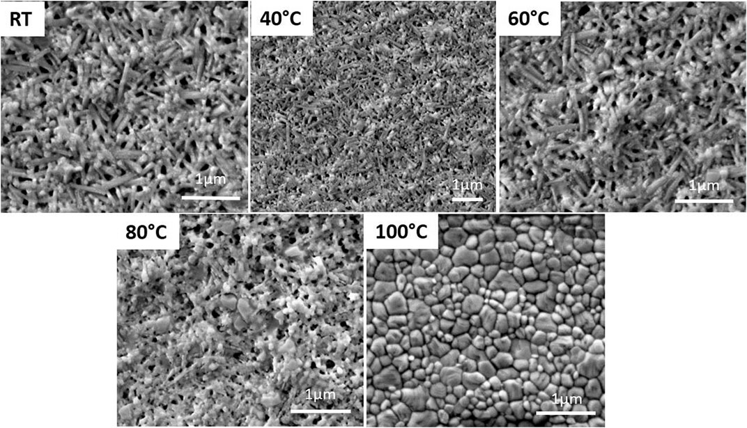
FIGURE 1. In situ scanning electron microscopy images showing morphological transformation of MAPbI3 film at different temperatures from room-temperature (RT) to 100°C.
This in situ SEM experiment was corroborated by in situ X-ray diffraction study as a function of temperature to determine the film’s structural change (Figure 2). The first X-ray diffraction pattern, recorded at room temperature, shows four prominent diffraction peaks at 2θ = 9.33°, 18.59°, 25.30° and 39.95° in addition to those corresponding to the FTO-based glass substrate. These diffraction peaks cannot be ascribed to the tetragonal I4/mcm space group of MAPbI3 phase at room temperature, (Whitfield et al., 2016) nor to PbI2 or MAI used as precursors. They are attributed to the formation of an intermediate phase involving the precursors and the solvent (DMF/DMSO). (Jo et al., 2016) Although there is no clear morphological change as seen by SEM, heating to above 40°C causes modification in the film’s structure, i.e. decrease of the intermediate phase in favour of the formation of the perovskite structure with the onset growth of the (110), (220) and (310) reflections. These diffraction peaks are becoming narrower and more intense above 60°C. The film crystallizes with a preferential orientation along the (hh0) planes as often observed in the literature. (Docampo et al., 2014; Song et al., 2015) This direction corresponds to the denser plane of the perovskite structure containing lead and iodide slabs. Table 1 gathers the evolution of the crystallite size corresponding to the (110) direction as a function of the annealing temperature using Scherrer equation. The lanthanum hexaboride was used as a standard sample (no strain or size broadening) to substract the instrumental broadening contribution from the FWHM. A slight shift to lower angles of the (hh0) diffraction peaks is observed due to thermal expansion of the perovskite lattice with the temperature (Figure 2).
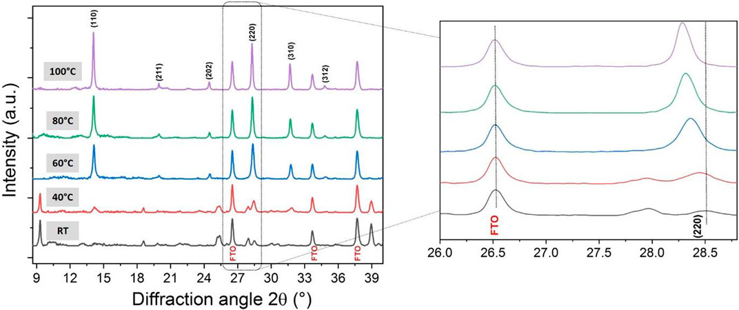
FIGURE 2. (A) In situ X-ray diffraction study as a function of temperature for a spin-coated film of 1:1 ratio of MAI and PbI2. The inset shows the (220) diffraction peak shift of MAPbI3.
TABLE 1. Evolution of the crystallite size of MAPbI3 as a function of the annealing temperature (in situ) from room-temperature (RT) to 100°C.
In addition to these in situ investigations, providing direct insights on the early-stage processes on film’s crystallization and morphological change, ex situ experiments combining XRD and SEM analysis were also performed to cover the range of temperatures above 100°C (Figure 3). For this, the annealing process was carried out for 30 min in an Ar-filled glovebox, corresponding to the typical crystallization method reported in the community to reach a film with a high optical quality.
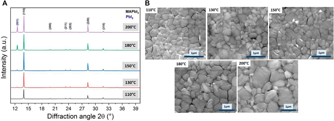
FIGURE 3. (A) Evolution of the X-ray diffractograms as a function of the annealing temperature between 110°C and 200°C for 30 min in Ar-filled glovebox and (B) corresponding top-view SEM images of the resulting film.
The temperature increase leads to a stronger preferential orientation along (hh0) planes family coming conconmitantly with a narrowing of the (110) diffraction peak, which results from larger crystallite size reaching 210 nm for this out-of-plane direction (Table 2). This observation correlates well with the top view SEM image showing well-visible grain growth in-plane of the FTO glass substrate (Figure 3B). The commonly shared wisdom regarding film’s morphology is that larger grains are beneficial for the device performances. (Choi et al., 2020) It limits the number of grain boundaries, which are one seat for non-radiative recombination losses due to shallow surface traps. (Gao et al., 2019a) Surface defects, including grain boundaries, play a significant role in the moisture-induced degradation of MAPbI3. (deQuilettes et al., 2017; Akhavan Kazemi et al., 2020; Krishna et al., 2020) Limiting the number of grain boundaries within the film’s thickness is primordial to ensure efficient carriers collection. (Xiao et al., 2014; Li et al., 2016; Gao et al., 2019b) Therefore, a film’s preferential orientation along (hh0) planes combined with high uniformity and larger grain size would be beneficial for higher diffusion length of the photo-generated carriers towards the selective contacts, which is one important feature for high photovoltaic performances. (Leblebici et al., 2016; Zhang et al., 2016)
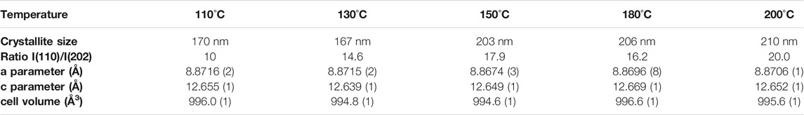
TABLE 2. Evolution of crystallite size, the ratio between (110) and (202) diffraction peak intensities and the ratio between (110) of MAPI and (001) of PbI2 as a function of the annealing temperature of MAPI films annealed between 110–200 °C.
However, although higher annealing temperatures still improve the film’s quality, increasing the annealing temperature to above 130°C leads to the onset of a competitive process niche in a decomposition reaction leading to PbI2 in the film (2θ = 12.69°) and MAI gas release. This reaction is facilitated by the high volatility of methylammonium iodide at this temperature. Slight modifications of the lattice cell parameters are observed depending on the post-annealing temperature leading to a cell volume in the range of 996 Å3. This slight fluctuations indicate that the bulk film stoichiometry may vary slightly.
The influence of the post-annealing temperature on the films’ optical characteristics was evaluated by UV-Visible absorption spectroscopy (Supplementary Figure S1). For all temperatures, the as-prepared MAPbI3 films exhibited a strong light absorption from 400 to 780 nm, indicating panchromatic light harvesting. A sharp increase in absorbance is observed, starting from 40°C to higher temperatures which is associated visually to a transition from a brown semi-transparent to a black mirror feature. At RT and 40°C, we can notice an absorption band at 400 nm. It is attributed to the unreacted precursors and/or the coordinated intermediate phase involving PbI2 and the solvent (DMF/DMSO), in agreement with the XRD peak at 2θ = 9.33° showed in Figure 2. Upon increasing the temperature to 140°C, a noticeable increase in the optical absorbance of MAPbI3 (below ca. 600 nm) is observed. For higher temperatures, it decreases by about half magnitude owing to the formation of the yellow PbI2 phase. The optical bandgap, deduced from the tauc plot (Supplementary Figure S2), narrows slightly from 1.60 eV for the temperatures below 100°C, 1.59 eV for the temperature range between 100°C and 180°C and reaches 1.58 eV at 200°C (Supplementary Table S1). The PL spectra also show slight but visible variations between 770 and 780 nm depending on the post-annealing temperature. The full width at half maximum of the PL band becomes narrower when crystallized, more symmetrical and more intense with temperature. However, this is associated with an increase of Urbach energy from 59.5 to 103.5 meV with the temperature, thus indicating that the latter causes more surface electronic disorder which may affect the photovoltage and fill factor values.
The radiative recombination dynamic of MAPbI3 depending on the annealing temperature has been studied using Time-Correlated Single Photon Counting (TCSPC) technique (Figure 4). This study has been carried out on a film deposited upon glass substrate. For the sake of clarity, we herein selected three type of films. One for an annealing temperature of 100°C, one at a lower temperature (i.e. 60°C) which represents a pivotal temperature for the film crystallization as abovementioned, and a last one at a higher temperature (i.e., 150°C) which represents a region where PbI2 starts to be formed.
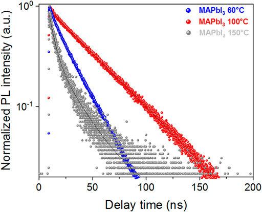
FIGURE 4. Evolution of PL decay measured by Time-Correlated Single Photon Counting (TCSPC) technique using 475 nm excitation (2 MHz, 100 nJ cm−2 fluence), 775 nm emission (slit opening 10 nm) with a 645 nm long-pass filter for MAPbI3 prepared at 60°C, 100°C and 150°C.
For the film prepared at 100°C, the PL decay is very close to a mono-exponential feature. It has a minor contribution of 8% in fraction leading to a τ1 = 4.2 ns and a predominant slower contribution τ2 = 41.4 ns. This leads to an average lifetime <τavg> = 38.4 ns (Table 3). Two contributions have been largely reported in the literature. (Son et al., 2016; Lee et al., 2017) Based on literature and our previous observations (Akhavan Kazemi et al., 2020), the fast component is attributed to the dynamic of carriers trapping at the surface and/or at the grain boundaries. The latter is largely influenced by the laser fluence, surface passivation and the interface between the perovskite grains and the environment. The slow component corresponds to the Shockley-Read-Hall recombination dynamic in bulk. For the film prepared at lower temperature, a single exponential decay is observed with a half-time of τ = 18.2 ns. For higher temperature, the PL decay becomes more clearly bi-exponential with the predominance of the fast component with same half-time; i.e., τ1 = 4.3 ns (f = 62%) and a slow contribution τ2 = 20.3 ns (<τavg> = 10.5 ns). For this film, the PL yield is reduced which is at the origin of the dispersity in the data points. These results suggest that PbI2 as a degradation by-product and higher annealing temperatures create surface/grain boundaries carriers trapping and accelerate the radiative bulk recombination despite the formation of larger grains as observed by SEM. This result correlates with the Urbach energy increases.
TABLE 3. Summary of the PL characteristics obtained after reconvolution from IRF for MAPbI3 depending on the crystallization temperature.
The impact of the annealing temperature on the device performance has been investigated in a n-i-p mesoscopic cell configuration. Figure 5 gathers the (J-V) curves of the champion cell for the perovskite layer prepared at 100°C and for the two extremum temperatures, and, the evolution of the cell characteristics as a function of the post-annealing temperature. The different characteristic values are reported in Supplementary Table S2. The annealing process was carried out for 30 min. The results show primarily two domains. The first lies between room-temperature and 60°C. In this range, both the cell photovoltage and photocurrent are increasing very rapidly with temperature. This correlate with the noticeable morphological evolution and perovskite structure crystallization as aforementioned. The cell photovoltage reaches a maximum of 1.04 V for an annealing temperature of 100°C. Below and above this temperature, the open circuit voltage is in the range of 1.00 V, except when the perovskite film is not crystallized even though the latter still exhibits a remarkable value of around 0.90 V. By contrast to the deliberate introduction of PbI2 excess in the precursor solution leading to PbI2 grains in the film and located at grain boundaries which are reported to alleviate surface defects, when the latter is issued from MAPbI3 decomposition, its consequence into the device performance is totally different. It does not produce any photovoltage gain. In opposite, it decrease the latter owing to more defects creation. A similar evolution is observed for the fill factor, at the exception of the maximum that is reached at a temperature of 90°C. Well-crystallized, large and defective-free grains of MAPbI3 are key parameters to reach higher fill factor and photovoltage values as herein suggested. Interestingly, besides for the amorphous film, the cell photocurrent is a parameter much less sensitive to the annealing temperature. Our devices generate in average a photocurrent value of ca. 22.5 mA/cm2 with a maximum of 24.0 mA/cm2 for the film crystallized at 130°C and 200°C (Figure 5B). The statistical analysis is shown in Supplementary Figure S3. This result led us to the conclusion that the film’s crystallinity plays the major role for the photocurrent generation and is not drastically affected by the formation of PbI2 subsequently to the thermal decomposition of MAPbI3.
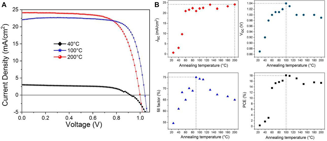
FIGURE 5. (A) (J-V) curve under AM1.5G conditions of MAPbI3-based devices with different annealing temperatures: 40°C, 100°C and 200°C, during 30 min. (B) Evolution of the cell characteristics as a function of the annealing temperature of MAPbI3. (scan rate: 10 mV s−1; area: 0.09 cm2; without any prior light soaking or pre-treatment applied to the devices).
This work underlines the existing temperature trade-off between increasing the post-annealing temperature for promoting large, well-packed and well-crystallized MAPbI3 grains and onset of its thermal decomposition into PbI2 in the film and MAI releases. With the aim to explore a protocol to combine the best of the high temperature annealing, we investigated the effect of time for a post-annealing temperature of 200°C from 30 s to 5 min. Surprisingly, a post-annealing of only 30 s affords to have pinhole-free and well-crystallized MAPbI3 film (Figure 6). Although it has been discussed in literature that a very fast crystallization of MAPbI3 can be beneficial to form randomly oriented grains (Dong et al., 2015), in our case, the results show already a strong preferential orientation of the grains along (110) direction. Prolonging the annealing time leads to grain growth from ca. 200 nm to more than 1 µm as showed by the top-view SEM pictures (Figure 6B). Sharper diffraction peaks are also experienced with time. The crystallize size is increasing from 152 to 222 nm along the (110) direction without affecting significantly the preferential orientation. PbI2 formation starts after ca. 3 min (Figure 6A). The PbI2 nanoparticles are well-visible on the SEM pictures leading to bright and small nanocrystals of ca. 100 nm size. They are principally formed at grain boundaries between the MAPbI3 grains and we hypothesized that there are formed preferentially on top of the film and not inner considering the difficulties to release MAI from bulk (Figure 6B).
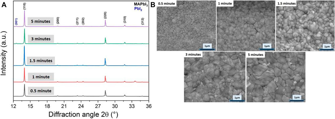
FIGURE 6. (A) Evolution of X-ray diffractograms for a film of MAPbI3 post-annealed at 200°C for different times from 0.5 to 5 min, (B) High magnification top-view SEM images of the corresponding films.
The evolution of steady-state PL for the different annealing time shows that the highest intensity is obtained for 1.5 min with a maximum of PL at 780 nm (Supplementary Figure S4). For longer time, the PL rapidly drop, thus suggesting that extended exposure irreparably causes the formation of non-radiative recombination pathways, likely bulk/surface shallow traps. As for temperature effect, lower crystalline perovskite leads to a broad and blue-shifted emission at ca. 770 nm.
As one could expect, there is an important influence of the annealing time on the photovoltaic performances (Figure 7; Table 4). The best PCE is obtained for a post-annealing time of 1.5 min leading to a value of 18.8% under AM1.5G conditions (Voc = 1.06 V, Jsc = 25.0 mA/cm2 and FF = 72.0%). These values are improved compared to the conventional and milder annealing temperature of 100°C for 30 min, thus highlighting the relevance of examining flash post-annealing procedure. This is actually the best compromise found between large perovskite grains, low level of non-radiative defects while avoiding perovskite decomposition into PbI2. Based on the cell characteristics evolution, we support similar conclusions as above, namely the low crystallinity mainly affects the cell photocurrent whereas onset of perovskite decomposition into PbI2 mainly penalizes the cell photovoltage and the fill factor values. The preconceived opinion that the largest grain size from top-view SEM pictures is a guarantee of high device performance is probably simplistic. The level of grain boundaries seems having here limited consequences on the cell photovoltage and the fill factor and the high crystallinity of the grain is a more important factor to consider in agreement with Liu et al. (Ren et al., 2016) Compared to the 100°C for 30 min post-annealing condition, the cross-sectional SEM picture reported in Supplementary Figure S5 shows that grain boundaries are more perpendicularly oriented to the substrate in the case of this flash annealing. This is finally consistent with the larger crystallite size determined for the [110] direction which reaches 196 nm, a value more comparable to the film’s thickness, compared to 123 nm for the first condition.
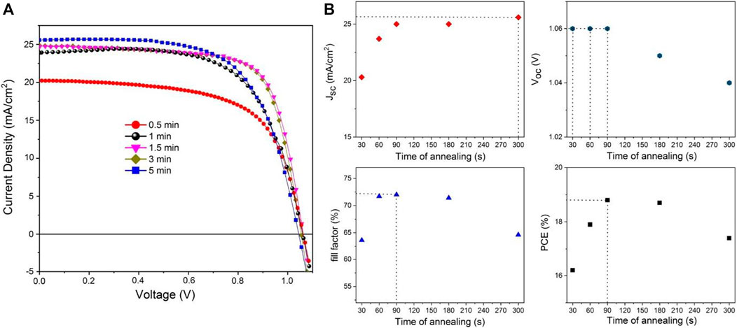
FIGURE 7. (A) Evolution of the (J-V) curve of MAPbI3-based devices prepared with a post-annealing of 200°C for different annealing time, (B) Evolution of the cell characteristics (Voc, Jsc, FF and PCE) as a function of annealing time. (scan rate: 10 mV s−1; area: 0.16 cm2; without any prior light soaking or pre-treatment applied to cell).
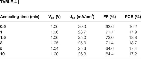
TABLE 4. Summary of the cell characteristics measured under AM 1.5G conditions for MAPbI3 films crystallized at 200°C for different annealing time.
Conclusion
This holistic study establishes the relationship between the post-annealing temperature and time for the crystallization of MAPbI3 on the textural, opto-electronic properties and device characteristics under AM1.5G conditions. The textural properties of the perovskite are closely related to the post-annealing conditions. The latter controls the competitive process between crystal growth and high crystallinity, an important asset to reach high photocurrent value, and MAPbI3 decomposition into PbI2 which in turn affects both the cell photovoltage and the fill factor values. Higher temperatures accelerate the formation kinetic of MAPbI3, produces a perovskite film with higher crystallinity, stronger preferential orientation along (hh0) planes and larger grains. However, it prompts also its decomposition into PbI2 and MAI gas release. For temperatures above 130°C for 30 min, this thermal treatment creates non-radiative defects responsible for fill factor and photovoltage decrease. Optimal conditions, considering such two antagonists processes (high crystallinity vs thermal decomposition), were obtained at 100°C for 30 min leading to a device exhibiting 18.0% PCE. However, flash annealing, combining a high post-annealing temperature of 200°C with very short annealing time (1.5 min), leads to a film exhibiting the best textural properties and at same time the highest PCE value of 18.8%. This improvement is mainly attributed to the obtaining of well-crystallized films composed of grains having limited amount of grain boundaries out-of-plane while having not the time to seed the thermal decomposition into PbI2 and MAI.
Materials and Methods
Materials: Unless specified, all chemicals were purchased from Sigma-Aldrich. Mesoporous TiO2 paste and FK209 were purchased from Greatcell solar materials. PbI2 and MAI were purchased from TCI.
Thin film fabrication: Glass substrate or FTO (TEC11L) were used. They were systematically cleaned with 2 vol% of hellmanex solution in DI water, isopropanol, acetone and treated with UV/O3 cleaner for 15 min prior being used. The precursor solution was prepared by dissolving 1 mol/L MAI (159 mg), 1 mol/L PbI2 (461 mg) in anhydrous N,N-dimethylformamide and anhydrous dimethylsulfoxide with 4:1 volume ratio. The solution was kept under stirring overnight at 70°C and then cooled down to ambient temperature. The solution was spin-coated (Laurell Spin coater WS-650hz) according to a two-step procedure inside an Ar-filled glovebox (MBraun Unilab Pro SP), first at 1,000 rpm for 10 s and then at 4,000 rpm for 20 s. During the second step, 1 ml of toluene as an anti-solvent was dropped 10 s before the end of the program. These films were annealed inside the same Ar-filled glovebox at different temperatures and for 30 min. The crystallization of the perovskite structure leads to a mirror-like dark film. This procedure has been optimized to reach the highest power conversion efficiency in full devices.
Device Fabrication: FTO glass substrate (NSG10) was cleaned according to the same procedure as aforementioned. A compact TiO2 blocking layer is deposited by spin-coating using a 0.15 mol/L titanium diisopropoxide bis(acetylacetonate) (75%) in 1-butanol (3,000 rpm for 30 s). The film is annealed at 125°C for 5 min. A second layer is deposited with 0.3 mol/L titanium diisopropoxide bis(acetylacetonate) solution in 1-butanol with same procedure. After this, the substrates were heated at 450 C for 30 min to form a compact layer of TiO2 of ca. 50 nm thickness. A 200 nm mesoporous TiO2 layer is deposited by spin coating at 4,000 rpm for 30 s with a ramp of 1,000 rpm s−1 from the commercially available TiO2 paste diluted in ethanol (6:1 weight ratio). After spin coating, the substrate is immediately dried at 120°C during 10 min. The substrate is then sintered at 500°C for 30 min before the deposition of the perovskite layer. The precursor solution was prepared by dissolving 1 mol/L MAI (159 mg) and 1 mol/L PbI2 (461 mg) in anhydrous N,N-dimethylformamide (0.8 ml), and anhydrous dimethylsulfoxide (0.2 ml). These solutions were then spin-coated in a two-step procedure at 1,000 rpm for 10 s and 4,000 rpm for 20 s, respectively. During the second step, 1 ml of toluene was dropped 10 s before the end of the program. These spin-coated perovskite films were annealed at different temperatures for 30 min inside an Ar-filled glovebox.
Films and Device Characterization: The (J–V) characteristics were recorded by means of a Keithley computer-controlled digital source meter (2412A) combined with a 3A class Newport SOL3A sun simulator with an AM 1.5G filter (100 mW/cm2). The light intensity was calibrated with a NREL-certified KG5-filtered Si reference diode. The photo-active area is 0.09 cm2 defined by a 3D printed black mask. The scan direction is reverse.
X-ray diffraction study was carried out at room temperature on a Bruker D8 diffractometer using a copper anti-cathode (λCuKα1=1.54056 Å and λCuKα2 = 1.54439 Å) and LynxEye detector. Each patterns were collected in 30 min between 2θ = 10° to 40° with a step size of 0.01°. The in situ measurement was carried out using an Anton Paar HTK furnace.
Scanning electron microscopy images were obtained using an environmental FEI Quanta 200 FEG microscope. Freshly spin-coated and not-annealed film was transferred from argon-filled glovebox into the SEM chamber and high vacuum operating condition established. During the transfer, the film was kept inside a transferring argon-filled box. The morphological evolution was followed in situ by gradually increasing the temperature of the sample holder. The UV-Visible absorption spectra were recorded in transmittance mode using an Agilent Cary5000 UV-Vis-NIR spectrometer. TCSPC experiments were carried out on Edinburgh Instrument FLS980 spectrometer using picosecond 475 nm laser diodes as an excitation source (2 MHz, 100 nJ cm−2 fluence), at 775 nm emission with a 645 nm long pass filter and slit size of 10 nm. A microchannel plate photomultiplier tube (MCP-PMT) Hamamatsu detector is set after the first emission monochromator. The measurements were carried out in front-face configuration. The typical instrument response function (IRF) value in this configuration is ca. 80 ps The steady-state PL spectra were measured using the same spectrometer with a continuous xenon arc lamp (450 W) equiped with a double excitation and double emission monochromators to reach stray light rejection less than 10−10 (excitation/emission bandwidth of 3 nm). The samples were excited at 450 nm and the emission detected by a high-gain photomultiplier tube (PMT) detector mounted after the second emission monochromator. For both steady-state PL and TCSPC measurements, the perovskite film was deposited on a clean glass substrate, and the samples were excited front to the perovskite layer.
The PL decays were fitted, after reconvolution from the IRF, using either a mono-exponential function or when needed a bi-exponential function to account from traps filling in the form of :
where τ1 and τ2 are the half-time constants, and A1 and A2 are their corresponding pre-exponential factors. The average lifetime is obtained as following:
where,
Data Availability Statement
The original contributions presented in the study are included in the article/Supplementary Material, further inquiries can be directed to the corresponding author.
Author Contributions
MK conducted most of the experiments and provided first draft of the article. AJ assisted MK for the in situ SEM experiments. FS has supervised the work and finalized the article.
Funding
This work has received financial support from Région Hauts-de-France, FEDER and Electricité de France (EDF) through the program PEROVSTAB.
Conflict of Interest
The author declares that the research was conducted in the absence of any commercial or financial relationships that could be construed as a potential conflict of interest.
The handling editor declared a past co-authorship with authors MAAK, FS.
Publisher’s Note
All claims expressed in this article are solely those of the authors and do not necessarily represent those of their affiliated organizations, or those of the publisher, the editors, and the reviewers. Any product that may be evaluated in this article, or claim that may be made by its manufacturer, is not guaranteed or endorsed by the publisher.
Acknowledgments
We thank Dr. Carine Davoisne and the electronic microscopy platform of UPJV for access to SEM microscope and for the fruitful discussion in designing the experiments. Dr. Jean Rousset (EDF) and Dr. Sébastien Gottis (LRCS) are also acknowledged as part of this work.
Supplementary Material
The Supplementary Material for this article can be found online at: https://www.frontiersin.org/articles/10.3389/fenrg.2021.732886/full#supplementary-material
References
Aharon, S., Dymshits, A., Rotem, A., and Etgar, L. (2015). Temperature Dependence of Hole Conductor Free Formamidinium lead Iodide Perovskite Based Solar Cells. J. Mater. Chem. A. 3, 9171–9178. doi:10.1039/c4ta05149a
Akhavan Kazemi, M. A., Raval, P., Cherednichekno, K., Chotard, J. N., Krishna, A., Demortiere, A., et al. (2020). Molecular‐Level Insight into Correlation between Surface Defects and Stability of Methylammonium Lead Halide Perovskite under Controlled Humidity. Small Methods 5 (2), 2000834. doi:10.1002/smtd.202000834
Best Research-Cell Efficiency Chart (2019). | Photovoltaic Research | NREL. Available at: https://www.nrel.gov/pv/cell-efficiency.html (accessed Sep 23, 2019).
Brenner, T. M., Egger, D. A., Rappe, A. M., Kronik, L., Hodes, G., and Cahen, D. (2015). Are Mobilities in Hybrid Organic-Inorganic Halide Perovskites Actually "High"? J. Phys. Chem. Lett. 6, 4754–4757. doi:10.1038/natrevmats.2015.07
Choi, H., Choi, K., Choi, Y., Kim, T., Lim, S., and Park, T. (2020). A Review on Reducing Grain Boundaries and Morphological Improvement of Perovskite Solar Cells from Methodology and Material‐Based Perspectives. Small Methods 4 (5), 1900569. doi:10.1002/smtd.201900569
deQuilettes, D. W., Jariwala, S., Burke, S., Ziffer, M. E., Wang, J. T.-W., Snaith, H. J., et al. (2017). Tracking Photoexcited Carriers in Hybrid Perovskite Semiconductors: Trap-Dominated Spatial Heterogeneity and Diffusion. ACS Nano 11, 11488–11496. doi:10.1021/acsnano.7b06242
D’Innocenzo, V., Grancini, G., Alcocer, M. J. P., Kandada, A. R. S., Stranks, S. D., Lee, M. M., et al. (2014). Excitons versus Free Charges in Organo-Lead Tri-halide Perovskites. Nat. Commun. 5, 3586. doi:10.1038/ncomms4586
Docampo, P., Hanusch, F. C., Giesbrecht, N., Angloher, P., Ivanova, A., and Bein, T. (2014). Influence of the Orientation of Methylammonium Lead Iodide Perovskite Crystals on Solar Cell Performance. APL Mater. 2 (8), 081508. doi:10.1063/1.4890244
Dong, Q., Yuan, Y., Shao, Y., Fang, Y., Wang, Q., and Huang, J. (2015). Abnormal crystal Growth in CH3NH3PbI3−xClxusing a Multi-Cycle Solution Coating Process. Energy Environ. Sci. 8, 2464–2470. doi:10.1039/c5ee01179e
Dualeh, A., Tétreault, N., Moehl, T., Gao, P., Nazeeruddin, M. K., and Grätzel, M. (2014). Effect of Annealing Temperature on Film Morphology of Organic-Inorganic Hybrid Pervoskite Solid-State Solar Cells. Adv. Funct. Mater. 24 (21), 3250–3258. doi:10.1002/adfm.201304022
Eperon, G. E., Burlakov, V. M., Docampo, P., Goriely, A., and Snaith, H. J. (2014). Morphological Control for High Performance, Solution-Processed Planar Heterojunction Perovskite Solar Cells. Adv. Funct. Mater. 24 (1), 151–157. doi:10.1002/adfm.201302090
Galagan, Y. (2018). Perovskite Solar Cells: Toward Industrial-Scale Methods. J. Phys. Chem. Lett. 9 (15), 4326–4335. doi:10.1021/acs.jpclett.8b01356
Gao, F., Zhao, Y., Zhang, X., and You, J. (2019). Recent Progresses on Defect Passivation toward Efficient Perovskite Solar Cells. Adv. Energ. Mater. 10 (13), 1902650. doi:10.1002/aenm.201902650
Gao, L., Zhang, F., Xiao, C., Chen, X., Larson, B. W., Berry, J. J., et al. (2019). Improving Charge Transport via Intermediate‐Controlled Crystal Growth in 2D Perovskite Solar Cells. Adv. Funct. Mater. 29, 1901652–1901657. doi:10.1002/adfm.201901652
Haque, M. A., Troughton, J., and Baran, D. (2020). Processing‐Performance Evolution of Perovskite Solar Cells: From Large Grain Polycrystalline Films to Single Crystals. Adv. Energ. Mater. 10 (13), 1902762. doi:10.1002/aenm.201902762
Hsiao, K.-C., Jao, M.-H., Li, B.-T., Lin, T.-H., Liao, S. H.-C., Wu, M.-C., et al. (2019). Enhancing Efficiency and Stability of Hot Casting P-I-N Perovskite Solar Cell via Dipolar Ion Passivation. Acs Appl. Energy Mater. 2, 4821–4832. doi:10.1021/acsaem.9b00486
Jeong, J., Kim, M., Seo, J., Lu, H., Ahlawat, P., Mishra, A., et al. (2021). Pseudo-halide Anion Engineering for α-FAPbI3 Perovskite Solar Cells. Nature 592 (7854), 381–385. doi:10.1038/s41586-021-03406-5
Jo, Y., Oh, K. S., Kim, M., Kim, K.-H., Lee, H., Lee, C.-W., et al. (2016). High Performance of Planar Perovskite Solar Cells Produced from PbI2(DMSO) and PbI2(NMP) Complexes by Intramolecular Exchange. Adv. Mater. Inter. 3 (10), 1500768. doi:10.1002/admi.201500768
Johnston, M. B., and Herz, L. M. (2016). Hybrid Perovskites for Photovoltaics: Charge-Carrier Recombination, Diffusion, and Radiative Efficiencies. Acc. Chem. Res. 49 (1), 146–154. doi:10.1021/acs.accounts.5b00411
Kim, H.-S., Hagfeldt, A., and Park, N.-G. (2019). Morphological and Compositional Progress in Halide Perovskite Solar Cells. Chem. Commun. 55, 1192–1200. doi:10.1039/c8cc08653b
Krishna, A., Akhavan Kazemi, M. A., Sliwa, M., Reddy, G. N. M., Delevoye, L., Lafon, O., et al. (2020). Defect Passivation via the Incorporation of Tetrapropylammonium Cation Leading to Stability Enhancement in Lead Halide Perovskite. Adv. Funct. Mater. 30 (13), 1909737. doi:10.1002/adfm.201909737
Leblebici, S. Y., Leppert, L., Li, Y., Reyes-lillo, S. E., Wickenburg, S., Wong, E., et al. (2016). Facet-Dependent Photovoltaic Efficiency Variations in Single Grains of Hybrid Halide Perovskite. Nat. Energ. 1. doi:10.1038/nenergy.2016.93
Lee, J.-W., Bae, S.-H., Hsieh, Y.-T., De Marco, N., Wang, M., Sun, P., et al. (2017). A Bifunctional Lewis Base Additive for Microscopic Homogeneity in Perovskite Solar Cells. Chem 3 (2), 290–302. doi:10.1016/j.chempr.2017.05.020
Li, S.-S., Chang, C.-H., Wang, Y.-C., Lin, C.-W., Wang, D.-Y., Lin, J.-C., et al. (2016). Intermixing-Seeded Growth for High-Performance Planar Heterojunction Perovskite Solar Cells Assisted by Precursor-Capped Nanoparticles. Energ. Environ. Sci. 9, 1282–1289. doi:10.1039/c5ee03229f
Li, Z., Klein, T. R., Kim, D. H., Yang, M., Berry, J. J., Van Hest, M. F. A. M., et al. (2018). Scalable Fabrication of Perovskite Solar Cells. Nat. Rev. Mater. 3, 18017. doi:10.1038/natrevmats.2018.17
Liu, H., Liu, H., Yang, J., Yang, F., Liu, Z., and Jain, S. M. (2019). Improving the Performance of Planar Perovskite Solar Cells through a Preheated, Delayed Annealing Process to Control Nucleation and Phase Transition of Perovskite Films. Cryst. Growth Des. 19, 4314–4323. doi:10.1021/acs.cgd.9b00024
Liu, K., Liang, Q., Qin, M., Shen, D., Yin, H., Ren, Z., et al. (2020). Zwitterionic-Surfactant-Assisted Room-Temperature Coating of Efficient Perovskite Solar Cells. Joule 4 (11), 2404–2425. doi:10.1016/j.joule.2020.09.011
Liu, S., Guan, Y., Sheng, Y., Hu, Y., Rong, Y., Mei, A., et al. (2019). A Review on Additives for Halide Perovskite Solar Cells. Adv. Energ. Mater. 10 (13), 1902492. doi:10.1002/aenm.201902492
Nie, W., Tsai, H., Asadpour, R., Blancon, J.-C., Neukirch, A. J., Gupta, G., et al. (2015). High-Efficiency Solution-Processed Perovskite Solar Cells with Millimeter-Scale Grains. Science 347 (6221), 522–525. doi:10.1126/science.aaa0472
Ren, X., Yang, Z., Yang, D., Zhang, X., Cui, D., Liu, Y., et al. (2016). Modulating Crystal Grain Size and Optoelectronic Properties of Perovskite Films for Solar Cells by Reaction Temperature. Nanoscale 8 (6), 3816–3822. doi:10.1039/c5nr08935b
Saliba, M., Correa-Baena, J.-P., Grätzel, M., Hagfeldt, A., and Abate, A. (2018). Perovskite Solar Cells: From the Atomic Level to Film Quality and Device Performance. Angew. Chem. Int. Ed. 57 (10), 2554–2569. doi:10.1002/anie.201703226
Saliba, M., Matsui, T., Seo, J.-Y., Domanski, K., Correa-Baena, J.-P., Nazeeruddin, M. K., et al. (2016). Cesium-Containing Triple Cation Perovskite Solar Cells: Improved Stability, Reproducibility and High Efficiency. Energ. Environ. Sci. 9 (6), 1989–1997. doi:10.1039/c5ee03874j
Shi, D., Adinolfi, V., Comin, R., Yuan, M., Alarousu, E., Buin, A., et al. (2015). Low Trap-State Density and Long Carrier Diffusion in Organolead Trihalide Perovskite Single Crystals. Science 347 (6221), 519–522. doi:10.1126/science.aaa2725
Shi, D., Adinolfi, V., Comin, R., Yuan, M., Alarousu, E., Buin, A., et al. (2015). Low Trap-State Density and Long Carrier Diffusion in Organolead Trihalide Perovskite Single Crystals. Science 347 (6221), 519–522. doi:10.1126/science.aaa2725
Son, D.-Y., Lee, J.-W., Choi, Y. J., Jang, I.-H., Lee, S., Yoo, P. J., et al. (2016). Self-Formed Grain Boundary Healing Layer for Highly Efficient CH3NH3PbI3 Perovskite Solar Cells. Nat. Energ. 1 (7), 16081. doi:10.1038/nenergy.2016.81
Song, Z., Watthage, S. C., Phillips, A. B., Tompkins, B. L., Ellingson, R. J., and Heben, M. J. (2015). Impact of Processing Temperature and Composition on the Formation of Methylammonium Lead Iodide Perovskites. Chem. Mater. 27 (13), 4612–4619. doi:10.1021/acs.chemmater.5b01017
Whitfield, P. S., Herron, N., Guise, W. E., Page, K., Cheng, Y. Q., Milas, I., et al. (2016). Structures, Phase Transitions and Tricritical Behavior of the Hybrid Perovskite Methyl Ammonium Lead Iodide. Sci. Rep. 6 (June), 1–15. doi:10.1038/srep35685
Xiao, M., Huang, F., Huang, W., Dkhissi, Y., Zhu, Y., Etheridge, J., et al. (2014). A Fast Deposition-Crystallization Procedure for Highly Efficient Lead Iodide Perovskite Thin-Film Solar Cells. Angew. Chem. 126, 10056–10061. doi:10.1002/ange.201405334
Xing, G., Mathews, N., Sun, S., Lim, S. S., Lam, Y. M., Gratzel, M., et al. (2013). Long-Range Balanced Electron- and Hole-Transport Lengths in Organic-Inorganic CH3NH3PbI3. Science 342 (6156), 344–347. doi:10.1126/science.1243167
Zhang, F., and Zhu, K. (2020). Additive Engineering for Efficient and Stable Perovskite Solar Cells. Adv. Energ. Mater. 10 (13), 1902579. doi:10.1002/aenm.201902579
Keywords: perovskite solar cells (PSCs), annealing temperature, perovskite crystallization, CH3NH3PbI3 perovskite, holistic study
Citation: Ali Akhavan Kazemi M, Jamali A and Sauvage F (2021) A Holistic Study on the Effect of Annealing Temperature and Time on CH3NH3PbI3-Based Perovskite Solar Cell Characteristics. Front. Energy Res. 9:732886. doi: 10.3389/fenrg.2021.732886
Received: 29 June 2021; Accepted: 13 October 2021;
Published: 29 October 2021.
Edited by:
Anurag Krishna, École Polytechnique Fédérale de Lausanne, SwitzerlandCopyright © 2021 Ali Akhavan Kazemi, Jamali and Sauvage. This is an open-access article distributed under the terms of the Creative Commons Attribution License (CC BY). The use, distribution or reproduction in other forums is permitted, provided the original author(s) and the copyright owner(s) are credited and that the original publication in this journal is cited, in accordance with accepted academic practice. No use, distribution or reproduction is permitted which does not comply with these terms.
*Correspondence: Frédéric Sauvage, ZnJlZGVyaWMuc2F1dmFnZUB1LXBpY2FyZGllLmZy