 Mustafa Tahir
 Sideng Hu
 Xiangning He
- Department of Electrical Engineering, Zhejiang University, Hangzhou, China
Wide bandgap (WBG) devices are becoming increasingly popular due to their excellent material properties. WBG devices are commercially available in discrete and module packages. Many studies have investigated the design, structure and benefits of module packages. However, a comprehensive and in-depth overview of the discrete package is lacking. Discrete package has the advantages of flexibility, scalability and reduced cost; however, challenges of severe switching oscillations and limited current capacity are associated with it. This review encompasses the switching oscillations and limited current capacity issues of discrete devices. Switching oscillations are categorized in terms of voltage. The underlying oscillation mechanisms are explored in detail. For the current imbalance, the types, root causes and adverse effects in parallel-connected discrete devices application are reviewed. Besides, the most recent techniques to extract stray parameters are also explored. Finally, state-of-the-art methods to mitigate the switching oscillations and the current imbalance are summarized and evaluated. The performance improvement strategies discussed in this paper can assist researchers to better use the discrete package and can stimulate them to come up with new solutions.
1 Introduction
1.1 Overview of Discrete Package
Excellent material characteristics of WBG devices enable the high efficiency, high frequency and high power density design of power converters. They are commercially available in both discrete and module packages (CREE, 2021b; Infineon, 2021a; Infineon, 2021b; Rohm, 2021). Discrete and module packages are commonly used in low and high power applications, respectively. In medium power applications such as an electric vehicle (EV), both packages can be employed (Bertelshofer et al., 2019; Lu, 2020; Infineon, 2021c). Module packages have advantages of high current ratings and low package inductance (Chen et al., 2017; Hou et al., 2020; Lee et al., 2020). However, they are expensive and lack design flexibility (Jahns and Dai, 2017; Bertelshofer et al., 2019; Lu, 2020). The discrete package features a cost-optimized solution and enables quick prototyping of available convert designs at different power levels (Bertelshofer et al., 2019; Lee et al., 2020). The flexibility facilitates the converter manufacturers to fulfill specific requirements. For instant, the discrete package is a good fit for the data center uninterruptible power supply (UPS) (Infineon, 2021c) and integrated motor drive inverters as it assists full integration (Jahns and Dai, 2017). Generally, for the same chip size, the available cooling area is larger in discrete package compared with module package as illustrated in Figure 1, which enables the device to better handle the fleeting overloading condition and can simplify the thermal design (Infineon, 2021c). With the advancements in packaging technology, new discrete packages such as TO-247PLUS offer higher power ratings and better thermal performance thanks to the bigger backside active thermal pad (Infineon, 2017; Infineon, 2021b; Sobe et al., 2020; IXYS, 2021). Finally, the discrete package is offered by more number of suppliers and it enables the designers to choose their preferred supplier based on price, region and customer support. The simple manufacturing process of discrete packages encourages the second sourcing strategies; thus, promoting the competition and as result, the price of discrete packages is expected to drop faster than that of module package. A 150 kW EV inverter with parallel-connected discrete (TO-247) SiC MOSFETs achieved a longer lifetime and similar power density compared to the Si module package (Bertelshofer et al., 2019). In addition, Tesla has also used discrete devices in parallel to push up the current ratings to achieve a cost-effective solution for EV inverters (Jahns and Dai, 2017; Jahns and Dai, 2018).
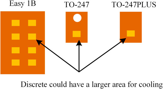
FIGURE 1. Comparison of available cooling area in module vs discrete package.
The discrete packages own the advantages of flexibility, scalability and reduced cost; though, challenges of severe switching oscillations and limited current capacity are associated with them. This review provides a comprehensive and in-depth overview of advanced performance improvement strategies to overcome these challenges.
1.2 Switching Oscillation Challenge
The high-frequency operation of WBG devices enables higher power density design by reducing the size of passive components. However, fast switching speed inevitably increases di/dt and dv/dt, inducing switching oscillations. The dv/dt of Silicon (Si) devices is typically around 3 V/ns (Ji et al., 2017) whereas that of Silicon Carbide (SiC) MOSFETs and Gallium Nitride (GaN) HEMT can reach 50 V/ns (Ji et al., 2017) and 80 V/ns (Hughes et al., 2012), respectively. Besides, low stray capacitance and the smaller RDSon of WBG devices aggravate the oscillations (Zhang W. et al., 2014; Huang et al., 2017; Wang et al., 2018). Oscillations get more severe in the discrete package due to the high parasitic inductance of the package and printed circuit board (PCB). These oscillations have adverse effects on the convert performance such as additional power losses (Abou-Alfotouh et al., 2006; Chen, 2009; Mermet-Guyennet et al., 2012; Chen, 2014; Nayak et al., 2014; Dong et al., 2015; Jahdi et al., 2015; Liang et al., 2019; Meng et al., 2019), increased EMI noise (Gong et al., 2013; Tsai et al., 2013; Zare et al., 2015; Fang et al., 2017; Zhang et al., 2019; Zhang and Wang, 2020), shoot through (Elbanhawy, 2005; Watanabe and Itoh, 2011; Xu et al., 2013; Yanagi et al., 2014; Zhang Z. et al., 2014; Ishibashi et al., 2015; Yin et al., 2016; Wang et al., 2018) and overshoots in current and voltage (Gamand et al., 2012; Joko et al., 2015; Ando and Wada, 2017; Liang et al., 2017).
1.3 Uneven Current Distribution Concern
High-power applications require high current ratings switching devices; however, the maximum current of a commercially available discrete SiC MOSFET is limited to 115A (CREE, 2021b; Infineon, 2021a; Rohm, 2021). To increase the current ratings, discrete devices are usually used in parallel for high-power applications (Bertelshofer et al., 2019). Due to a mismatch in the parameters of the devices (Wang G. et al., 2014; Ke et al., 2018; Zhao et al., 2021a; Zhao et al., 2021b) and asymmetrical layout design (Li et al., 2014a; Tiwari et al., 2015; La Mantia et al., 2017), the current distribution among parallel-connected discrete devices is uneven, leading to imbalanced power loss distribution, uneven temperature rise and risk of device thermal runaway.
Recently, several studies have been reported to address above mentioned issues, but a comprehensive overview of the discrete package is lacking. Previously published survey articles focus on different aspects (Millán et al., 2014; Wang and Zhang, 2016; She et al., 2017); analyze the performance and applications of WBG devices. Commercialization, design challenges and fabrication methods are discussed in Jones et al. (2016) and Zhao S. et al. (2021), active driving solutions for module packages are discussed in Zhao S. et al. (2021), packaging technology and progress of module packages are presented (Hou et al., 2020; Lee et al., 2020; Alizadeh and Alan Mantooth, 2021). A systematic overview of the discrete package offering performance improvement strategies is required to unleash its potential. This survey comprehends switching oscillations and uneven current distribution issues of discrete packages. Oscillations are classified in terms of drain to source voltage (Vds) and gate to source voltage (Vgs) and the underlying oscillation mechanism is explored in depth. In addition, the uneven current distribution is categorized into static current imbalance and dynamic current imbalance. Root causes and adverse effects of the current imbalance are also included. Furthermore, stray parameters extraction techniques are also discussed. In the end, the latest oscillation attenuation methods and current imbalance solutions are systematically summarized which can assist readers to fully leverage the benefits of the discrete packages.
2 Categories of Switching Oscillations
Switching oscillations have been reported in Si-based power converters (Idir et al., 2006; Makaran, 2009; Chen and Amaro, 2012; Filadelfo Fusillo, 2012; Taylor and Manack, 2012; Wang B. et al., 2014) which become even more severe in WBG devices because of their extremely low parasitic capacitances and fast switching speed. As shown in Figure 2A, all oscillation types along with their root cause are discussed in this section. Oscillations in Vds are organized as damped and sustained oscillation. Furthermore, oscillations in Vgs are discussed in terms of false turn-on and false triggering.
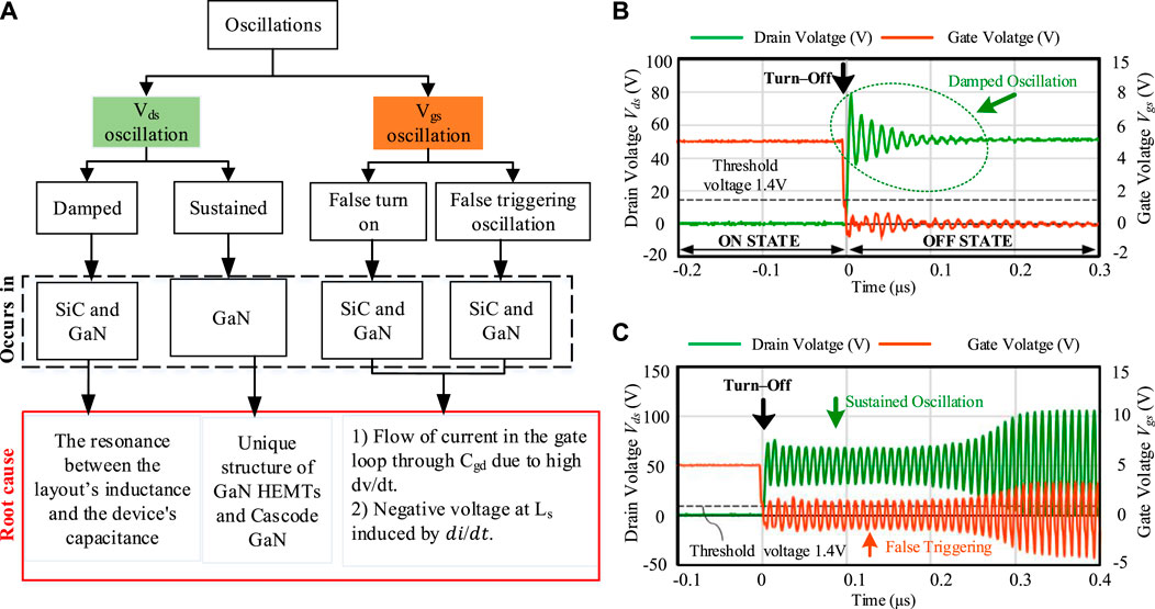
FIGURE 2. (A) Types of switching oscillations (B) Damped oscillation (C) Sustained oscillation (Umetani et al., 2019).
2.1 Drain to Source Voltage Oscillations and Underlying Mechanism
2.1.1 Damped Oscillations in Vds
The resonance between the inductance and capacitance in the power loop is a root cause of oscillation in Vds (Gamand et al., 2012; Nayak et al., 2014; Joko et al., 2015; Ando and Wada, 2017; Liang et al., 2017). A double pulse test (DPT) circuit is shown in Figure 3A, which is made up of a freewheeling diode and SiC MOSFET. The parasitic inductances in the circuit include; drain inductance (Ld), gate inductance (Lg), common source inductance (Ls) and loop inductance (Lloop). Besides, the parasitic capacitances include; drain to source capacitance (Cds), gate to drain capacitance (Cgd) and gate to source capacitance (Cgs). Parasitic capacitors and inductors might form an LC resonant circuit, then the energy transferred between them appears as an oscillation (Platania et al., 2011; Liu et al., 2016a). The oscillation gets damped over time as depicted in Figure 2B due to the small amount of resistance in the LC circuit which dissipates the energy in terms of heat. Damped oscillation is the most common type of oscillation and has been well documented in the literature. It has been reported in synchronous buck converters (Taylor and Manack, 2012), inverters (Chuai et al., 2019) and matrix converters (Safari et al., 2013). Oscillation can be modeled using RLC equivalent circuits (Kassakian and Lau, 1984; Teulings et al., 1996; Githiari and Palmer, 1998; Ogura et al., 2003; Palmer and Joyce, 2003; Fujihira et al., 2008; Makaran, 2009; Alatise et al., 2012; Chen and Amaro, 2012; Liu et al., 2016b; Ren et al., 2017; Ding et al., 2017). The turn-off equivalent RLC circuit for the inductive load testing circuit is studied in Liu et al. (2016a) and a mathematical model is provided for designing oscillation mitigation solutions.
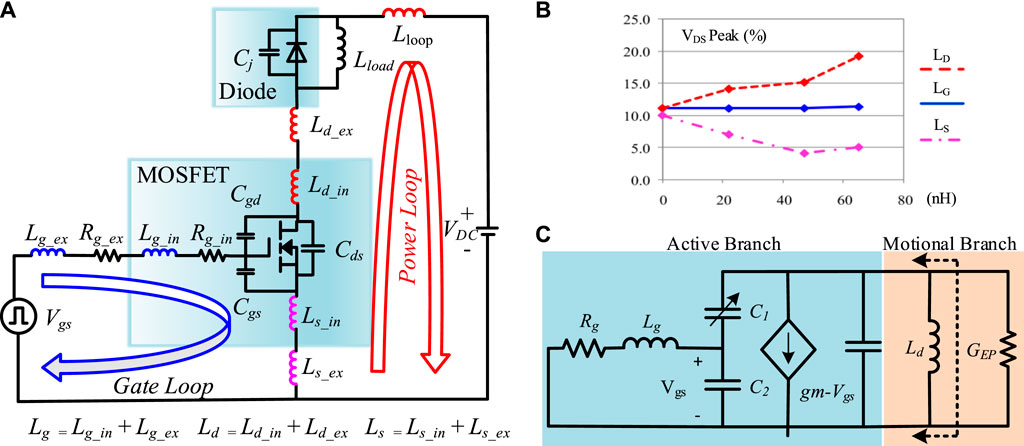
FIGURE 3. (A) Double pulse test (DPT) circuit (Liu et al., 2018b) (B) Effect of different parasitic inductances on the drain to source voltage (Vds) under the testing condition of 400 V and 10 A (Chen, 2009) (C) Equivalent small-signal model of DPT to investigate sustained oscillations (Lemmon et al., 2014).
In a complicated resonance process, the impact of individual inductances (Ld, Lg, Ls) on the oscillation is different. Analytical (Xiao et al., 2004; Ren et al., 2006; Zhang et al., 2008; Li et al., 2011; Wang et al., 2012; Alexakis et al., 2013; Raee et al., 2013; Takao and Ohashi, 2013; Azizouglu and Karaca, 2014; Nayak and Hatua, 2016; Xie et al., 2016) and empirical methods (Chen, 2009; Chen et al., 2010; Zhang et al., 2012; Chen et al., 2013a; Stewart et al., 2013; Wada et al., 2013; Anthon et al., 2014; Li and Munk-Nielsen, 2014; Noppakunkajorn et al., 2014; Noppakunkajorn et al., 2015; Walder and Yuan, 2015; Wang X. et al., 2017) have been reported that investigated the impact of different parasitic inductance on oscillation. As shown in Figure 3B, it is concluded that the impact of Lg on damped oscillation is negligible and the main contributor is Ld (Chen, 2009; Khanna et al., 2013). Larger Ld enables fast speed and reduced switching losses but elevates the oscillation in Vds. In addition, damped oscillation induced by the resonance of Ld and Cgd can be alleviated with increased Ls as it slows down the drain current. Larger Ls offers reduced oscillation and overshoots at the cost of increased switching losses.
2.1.2 Sustained Oscillations in Vds
Sustained oscillation in Vds stems out either from the structure of the device or sweep from the false triggering (Wang et al., 2009; Adamowicz et al., 2011; Xu et al., 2011; Chen et al., 2014; Arribas et al., 2015; Lemmon et al., 2015; Wang et al., 2018; Umetani et al., 2019). Sustained oscillations are commonly observed in GaN (Wang et al., 2018; Umetani et al., 2019) and less likely to occur in SiC devices thanks to their relatively higher Vth. Among GaN devices, the structure of normally-off GaN HEMT and cascode GaN can instigate sustained oscillation whereas the structure of SiC MOSFETs is not observed to have any contribution in sustained oscillations. For example, normally-off GaN HEMTs have a unique bidirectional channel in contrast to SiC MOSFET. One phase leg usually consists of a lower switch and an upper one. In the case of Si/SiC-based switches, when the lower switch is turned off, the current flows through the body diode of the upper switch (Wang et al., 2019). But in GaN HEMTs, when the lower switch is turned off, the reverse current flows through the channel of the upper switch due to the absence of the body diode. The reverse channel current in GaN HEMTs is governed by the source current and the device can draw energy from the source leading to a sustained oscillation (Wang et al., 2018). The condition for reverse conduction in GaN HEMTs is; Vgd > Vgd(th) or Vgs > Vgs(th), which implies that the device would conduct in the reverse direction when either Vgs or Vgd exceed their corresponding threshold voltage (Wang et al., 2018). Apart from normally-off GaN HEMTs, turn-off sustained oscillation also occurs in the cascode GaN devices. Cascode GaN is made up of a low resistance silicon MOSFET placed in series with a normally-on GaN HEMT to make it a normally-off device. The junction capacitance discrepancy between the two components causes sustained oscillation. Detailed analysis of sustained oscillation in the cascode GaN is presented in Huang et al. (2017) and authors have concluded that during the turn-off, the rise in the Vds of Si MOSFET might be caused by current oscillations. Then, a false turn on might occur in the internal GaN HEMT. This false turn-on of GaN HEMT causes sustained in the cascode GaN structure (Huang et al., 2017).
The susceptibility of sustained oscillation gets increased with larger transconductance and lower on-sate resistance of the device (Lemmon et al., 2014). Instead of using the hit and trial method, engineers usually predict sustained oscillation using the Barkhausen criterion and the small-signal models (Kazimierczuk, 2014; Lemmon et al., 2014; Umetani et al., 2019). Sustained oscillation would occur when the Barkhausen criterion is satisfied. A zero loop gain and the specified phase shift are required to fulfill the criterion (Unkrich and Meyer, 1982; Vittoz et al., 1988). To investigate the characteristics of the sustained oscillation, a small-signal model for the double pulse test (DPT) is presented in Figure 3C. The gate loop of the DPT act as the active branch and the power loop act as a motional branch (Lemmon et al., 2014). Sustained oscillations will occur if the resistance of the active branch is canceled out by the passive branch’s resistance and reactive parts counterbalance each other. It performs like a negative resistance case. Different methods to mitigate the oscillation are discussed in Section 4.
2.2 Gate to Source Voltage Oscillations and Underlying Mechanism
Gate to source voltage (Vgs) oscillation may cause false action like false turn-on or false triggering as shown in Figure 2A. Both of them may lead to a shoot-through issue. The shoot-through current deteriorates the performance, increases switching losses, and can even damage the devices (Elbanhawy, 2005; Watanabe and Itoh, 2011; Xu et al., 2013; Yanagi et al., 2014; Zhang Z. et al., 2014; Ishibashi et al., 2015; Fan et al., 2016; Yin et al., 2016; Wang et al., 2018). The difference between false turn-on and false triggering lies in single and repeated trigger action. The false turn-on is mainly related with the high dν/dt and di/dt in WBG devices (Khanna et al., 2013; Wang and Chung, 2014; Yanagi et al., 2014; Ishibashi et al., 2015; Jahdi et al., 2015; Wang et al., 2018; Li R. et al., 2019). When one of two MOSFETs in a phase leg configuration turns on, a fast-rising voltage appears across the off-state MOSFET, as shown in Figure 4. As a result, a current flow in the gate loop through Cgd causing a voltage drop. If the voltage drop is higher than the device threshold voltage, a false turn-on event would occur leading to shoot-through. Typically, the duration for a false turn-on is between 10 and 100 nsec (Yin et al., 2016) and the value of current can reach up to 150 A (Yanagi et al., 2014). As shown in Figure 3A, Ls stays in both gate loop and power loop. It indicates that a negative gate voltage would be introduced by high di/dt from power loop which can worsen the oscillation leading to false triggering. False triggering is reported in both SiC (Lemmon et al., 2013, 2014; Sugihara et al., 2017) and GaN (Umetani et al., 2016, 2019; Matsumoto et al., 2017) devices, though, the latter one is more susceptible to false triggering owing to its low threshold voltage. A comprehensive analysis of false triggering oscillations is provided in Umetani et al. (2016) and it is concluded that in order to avoid the false triggering oscillation the resonance frequency of the power loop and that of the gate loop should be decoupled. Besides, an optimum device selection and proper circuit layout design are important for depressing the gate oscillations by minimizing Cgd and Ls.
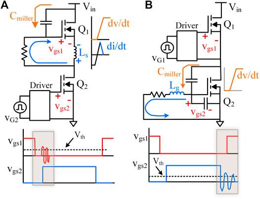
FIGURE 4. False turn-on due to gate to source voltage oscillation (A) When Q2 is turned on, high dv/dt appears across Q1 and flow of current through miller capacitor (Cgd) may false turn-on the Q1 (B) When Q2 is turned off and Q1 is turned on, high dv/dt appears across Q2 and flow of current through miller capacitor (Cgd) may false turn-on the Q2 (Wang et al., 2018).
3 Categories of Current Imbalance and Causes
Parameters of semiconductor devices vary even when they are from the same wafer. This variance is especially noticeable in WBG devices since technology is not yet mature. In Wang G. et al. (2014), thirty samples of SiC MOSFET (C2M0160120DA) from the same vendor under room temperature are evaluated and it has been reported that the difference of RDSon can reach up to 20% and the difference of Vth can reach up to 24% (Wang G. et al., 2014). The variation in the parameters of devices, called device mismatch, causes unequal current distribution (Wen et al., 2021; Zhao et al., 2021a; Zhao et al., 2021b). In addition, due to asymmetrical layout design, the discrepancy in the parasitic inductances of the circuit also causes uneven current distribution (Li et al., 2014a; Tiwari et al., 2015; La Mantia et al., 2017; Hu and Shao, 2021). During unequal current sharing, one device carries more current than the others, which not only stresses the device but may also lead to thermal runaway if it operates outside of its safe operating area (SOA).
3.1 Static Current Imbalance
Static current imbalance is due to the variation in RDSon of parallel-connected devices. During the on state, MOSFETs behave like a small resistor and a group of MOSFETs connected in parallel has the advantage of reduced resistance current path. Due to RDSon variation, the device with the lowest resistance conducts more current and has relatively higher conduction losses, as a result, its resistance increases. In Si MOSFETs, owing to the positive temperature coefficient (PTC) of RDSon, the static current imbalance naturally gets reduced (Xue et al., 2013; Mao et al., 2017a; Mukunoki and Horiguchi, 2018; Zeng et al., 2020). As shown in Figure 5E, the TO-247 package of Si, SiC and GaN MOSFETs with similar ratings have been tested. It is concluded that when the temperature is raised from 25°C to 175°C, the RDSon of Si, SiC and GaN increases by 3×, 1.5× and 2×, respectively. Hence, the intrinsic current sharing capability of WBG MOSFETs is not as prominent as that of Si counterparts (Wang G. et al., 2014; Xue et al., 2014a; Ke et al., 2018; Zeng et al., 2020; Zhao et al., 2021a; Zhao et al., 2021b). In addition, the value of gate to source voltage (Vgs) also influences the RDSon (Wang G. et al., 2014).
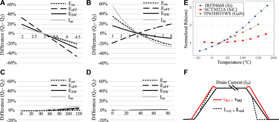
FIGURE 5. Effect of parameters discrepancy on the difference of switching losses between parallel-connected SiC MOSFETs (Timms, 2018) (A) Variation in Vth (B) Variation in Ls (C) Variation in Lg (D) Variation in Ld (E) Temperature impact on RDSon of Si, SiC and GaN in TO-247 package (Yadav and Nag, 2021) (F) Influence of Vth and Ls on drain current (Timms, 2018).
3.2 Dynamic Current Imbalance
The dynamic current of a device depends on its threshold voltage (Vth), gate to source voltage (Vgs) and transconductance (gfs) as depicted in Eq. 1. Among parallel-connected devices, the device with lower Vth or higher gfs conducts more dynamic current leading to dynamic current unbalance. Furthermore, dynamic current imbalance increases with a rise in temperature due to the negative temperature coefficient (NTC) of threshold voltage (Vth). At higher frequency, even a slight discrepancy in Ls of parallel-connected MOSFETs will induce negative feedback to gate voltage as revealed in Eq. 2, and the change in Vgs will directly impact the drain current as shown in Eq. 1.
Dynamic current imbalance leads to unequal distribution of switching losses among parallel connected devices. The impact on switching losses variation from the current imbalance is illustrated in Figures 5A–D (Timms, 2018). It shows that the dynamic current and switching losses distribution are mainly affected by the Vth and Ls. As demonstrated in Figure 5F (Timms, 2018), a lower Ls means a faster switching speed. In addition, a lower Vth means faster turns on but slower turns off. Hence, matching the Vth and Ls of parallel-connected devices is crucial to suppress the dynamic current imbalance.
In summary, the prominent root cause of static current imbalance is RDSon whereas the mismatch in Vth, Ls or gfs instigates the dynamic current imbalance. The adverse effects of the current imbalance include uneven power loss distribution, increased stress to a single device, higher current overshoots, uneven temperature rise and all contribute to reduced reliability.
4 Methods to Mitigate Oscillations
4.1 Parasitic Elements Minimization
4.1.1 Impact of the Package
Parasitic elements causing switching oscillations are related to the device package and PCB layout. It is challenging to switch SiC MOSFET faster than 10 ns without ringing in the TO-247-3 package (Li and Munk-nielsen, 2014) as it has 8 nH inevitable common source inductance (Ls) (Aikawa et al., 2017). By using a package with a kelvin source, the oscillations and overshoots can be reduced since the Ls can be bypassed as shown in Figure 6 (Li and Munk-nielsen, 2014; Lemmon et al., 2016). TO-247-4, TO-247PLUS-4 and TO-263-7 are the common commercialized package with a kelvin source. The TO-247PLUS-4 (CREE, 2021a) package offers a higher breakdown voltage (1,700 V) with superior thermal performance and increased current ratings. The TO-263 package offers 32% less package inductance than the TO-247 package and achieved 29% reduction in switching losses per cycle and reduced the current overshoot by 10 A in Lemmon et al. (2016). Hence, low package inductance and Kelvin source connection facilitate the oscillation mitigation.
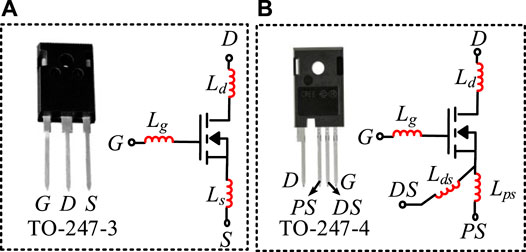
FIGURE 6. (A) Package without Kelvin connection (B) with Kelvin connection.
4.1.2 Impact of the Layout Design
Parasitic elements in the circuit also induce switching oscillations. An optimized layout design with respect to the loop size and geometry can reduce the overshoots and improves efficiency (Reusch and Strydom, 2014; Wang K. et al., 2017; Letellier et al., 2019; Sun et al., 2021). Parasitic inductances in the power and gate loops should be kept as low as possible to reduce switching oscillation. A comparison of different PCB layouts to minimize the power loop and drive loop inductances is presented in Wang K. et al. (2017). It is concluded that the double side layout achieves minimum power loop and drive loop inductance along with low voltage overshoot. A buck converter with a double-layer design achieves a 50% reduction in driver loop inductance, resulting in 0.6% increase in peak efficiency and 8.3% drop in drain-source voltage overshoot (Wang K. et al., 2017). To obtain an optimized layout design with minimized stray inductance, in-depth investigation has been carried out in Shtargot et al. (2012), Reusch and Strydom (2014), Meng et al. (2021), and Pace et al. (2021).
4.2 Gate Resistor Adjustment
The external gate resistor plays a critical role in the device’s performance. The dv/dt or di/dt of a device can be decreased by increasing the gate resistor (Rg), leading to a reduced oscillation and overshoots (Liu et al., 2016b) at the cost of increased switching losses. A detailed gate resistor effect demonstration is shown in Liu et al. (2018b), where an additional 10 Ω gate resistor brings a reduction of about 15 and 4% in voltage overshoot and oscillation duration, respectively. In another aspect, a significant increase in turn-on and turn-off times is resulted and the turn-on energy (Eon) and turn-off energy (Eoff) get increased by 64 and 80%, respectively. Gate resistor also impacts the false triggering oscillation and parasitic ringing, as reported in Gafford et al. (2013), Li and Munk-Nielsen (2014a), and Liu et al. (2018b). The gate resistor can be viewed as the tradeoff between switching losses and switching oscillations. To determine an optimum value of Rg, equivalent circuits, the analysis and validation are provided in Chen and Amaro (2012), Liu et al. (2016a), and Paredes et al. (2017).
4.3 Gate Driver Design
Adjustment of gate resistance can be viewed as a simple and specified way in gate driver to mitigate oscillations. Many well-designed gate drivers for oscillation and crosstalk depression are reported in the literature (Paredes Camacho et al., 2017; Paredes et al., 2017; Zhang et al., 2017). Gate drivers can be categorized as open loop gate drivers, active gate drivers and multi-level gate drivers.
4.3.1 Open Loop Gate Drivers
Conventional gate drivers (CGDs) are simple and work in the open loop. The cross-talk effect and oscillation caused by dv/dt or di/dt can be attenuated by employing negative voltage gate drivers (Kelley et al., 2009; Chen et al., 2011; CREE, 2011; Semiconductor, 2013; Li et al., 2020a). Nevertheless, negative voltage gate drivers induce negative overshoot in the Vgs and corresponding overshoot would affect the device reliability since the negative gate voltage withstand ability of WBG devices is low. Negative voltage spikes can be diminished using gate drivers with auxiliary transistors (Zhou and Gao, 2016; Gao et al., 2018). Reshaping the gate loop of conventional gate drivers with the implementation of two extra capacitors is another way to mitigate the cross-talk which achieved 0.6% increase in the converter’s efficiency by avoiding the Ls (Li Y. et al., 2019). An intelligent gate driver (IGD) adopting two auxiliary transistors and two diodes is reported in Zhang et al. (2017). Compared with conventional gate drivers, the intelligent gate driver offers similar oscillations attenuation with reduced energy losses and lower Vgs_peak, as shown in Figures 7A,B.
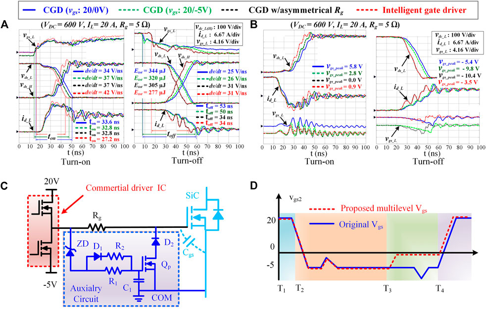
FIGURE 7. (A) Switching performance comparison of different conventional gate drivers (CGDs) with intelligent gate driver (B) Cross-talk comparison of conventional gate drivers and intelligent gate driver (Zhang et al., 2017) (C) Circuit diagram of multilevel gate driver (D) Waveform comparison of multilevel Vgs and original Vgs (Li et al., 2020b).
4.3.2 Active Gate Drivers
Active gate drivers mitigate the oscillation by actively controlling the gate voltage to regulate the slew rate of voltage/current. They employ a closed-loop to fully exploit the potential of WBG devices (Shahverdi et al., 2013; Dymond et al., 2018; Cao et al., 2021). The active gate driver proposed in Nayak and Hatua (2017) utilized stray inductance and capacitance to achieve quasi zero switching leading to reduced switching losses. To suppress the cross-talk, active gate drivers generally regulate the gate impedance and gate voltage. An active gate driver with gate assist circuits featured a fast turn-on by adjusting the gate loop resistance and gate voltage. It achieved up to 17% reduction in turn-on switching losses with an effectively suppressed cross-talk (Zhang Z. et al., 2014). Two gate assist circuits, gate impedance regulation and gate voltage control have been studied in Zhang Z. et al. (2014). Gate impedance regulation circuit is simple since it employs one transistor and one capacitor compared to gate voltage control circuit, which adopts two transistors and one diode (Zhang Z. et al., 2014). The former one is suitable for board-level integration and the latter one is a better fit for chip-level integration. Other active gate drivers that target Vds overshoot, EMI noise and parasitic ringing have been reported in Nayak and Hatua (2017), Paredes Camacho et al. (2017), Nayak and Hatua (2018), and Yang et al. (2019).
4.3.3 Multilevel Gate Drivers
Multilevel gate drivers are effective to mitigate crosstalk (Li et al., 2020b; Wu et al., 2020) and offer reduced energy losses and increased safety and reliability (Zhao et al., 2019; Li et al., 2020b). To introduce additional levels in gate voltage, multilevel gate drivers employ either auxiliary circuits or an active driving approach. A multilevel gate driver adopted an auxiliary circuit that is suitable to suppress false triggering oscillations and negative gate overvoltage (Li et al., 2020b). The auxiliary circuit is shown in Figure 7C which can easily be implemented on the conventional gate driver (Li et al., 2020b), as it does not require any additional dc power, isolation stage, or control signals. As shown in Figure 7D, during the Vgs positive peak event, the multilevel gate driver (Li et al., 2020b) keeps the voltage to a specific negative level so that false triggering can be avoided. Afterward, it shifts the voltage to zero or less negative level just before the positive peak event to prevent the negative voltage breakdown. Negative overshoot in the gate to source voltage is reduced from −9.9 V to −1.6 V (Li et al., 2020b). For desaturation protection, the multi-level turn-off strategy is widely used in the industry. In Zhao et al. (2019) an adaptive multi-level active gate driver is investigated that used a three-level turn-off strategy. It enables a shorter turn-off delay than conventional gate drivers and two-level gate drivers (Zhao et al., 2019). It employed a behavioral model and adaptive optimization to accommodate the variation in turn-off delay due to varying load currents and bus voltages.
To sum up, open loop gate drivers are relatively simple and their mitigation effect can be improved by employing additional components but still, they do not consider load variations. Active gate drivers and adaptive multi-level active gate drivers consider the load variation and provide effective oscillations mitigation, but have increased cost and design complexity (Paredes Camacho et al., 2017; Dymond et al., 2018; Zhao et al., 2019).
4.4 RC Snubbers
To suppress the oscillation, the large gate resistance increases the energy losses and the active gate driver approach demands complex feedback control. RC snubber offers reduced cost and complexity compared with the active gate driver and slightly less energy losses compared with the gate resistance method. RC snubber is a widely adopted solution for oscillation attenuation (McMurray, 1972; Josifović et al., 2011; Josifovic et al., 2012; Salem and Wood, 2014; Vaculik, 2014; Joko et al., 2015; Liu et al., 2016a; Liu et al., 2016b; Torsæter et al., 2016; Chen et al., 2021; Yang et al., 2021). Choosing optimum values of snubber for effective oscillation suppression is essential. An efficient way to design these parameters is to simplify the switching circuit into an equivalent RLC circuit incorporating all circuit parasitic. Then switching oscillations can be modeled using the RLC equivalent circuit and theoretical analysis of models can provide the guidelines for designing RC snubber. The equivalent RLC circuit of DPT including snubber is shown in Figure 8A. Snubber design methods can be categorized into second order, third order and higher order. Compared with the second order method, third order and higher order design methods enable better oscillation mitigation in both Vds and Vgs as depicted in Figures 8B,D at the cost of increased design complexity (Chen et al., 2020). Detailed guidelines to design snubber using second order approach are provided in Josifović et al. (2011), Josifovic et al. (2012), Salem and Wood (2014), Vaculik (2014), Joko et al. (2015), and Torsæter et al. (2016) and those for third order and higher order methods are discussed in Yatsugi et al. (2018) and Chen et al. (2020).
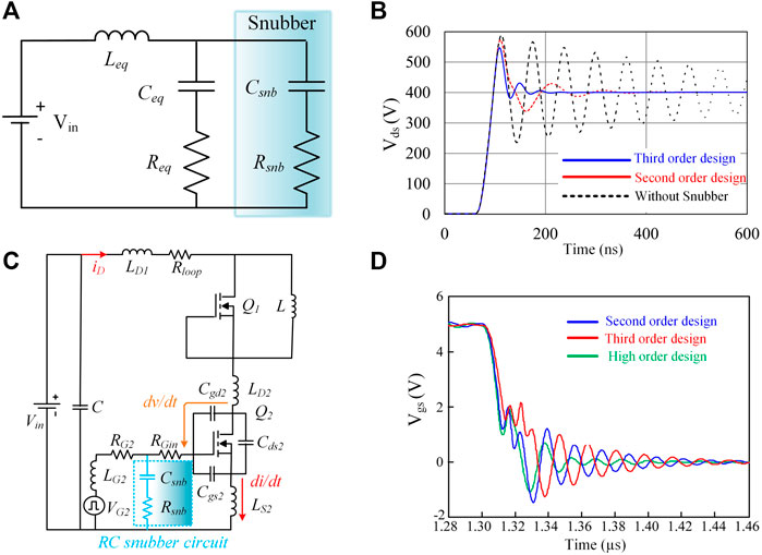
FIGURE 8. (A) Equivalent RLC circuit of DPT with snubber employed across the phase leg (B) Comparison of different design methods for oscillation attenuation in Vds (Yatsugi et al., 2018) (C) Circuit diagram of DPT with snubber employed in the gate loop (Chen et al., 2020) (D) Comparison of different design methods for false triggering mitigation (Chen et al., 2020).
4.5 Soft Switching Strategy
Switching oscillation and switching losses can also be mitigated by implementing either the zero voltage switching or zero current switching or both (Hua et al., 1994; Watson et al., 1996; Lai, 1997; Tang et al., 1998; Zhang et al., 2007; Chen et al., 2013b; Chen et al., 2013c; Ahmed et al., 2017). Usually, an additional capacitor/inductor or their combination is implemented in the topology to realize resonance for achieving soft switching. Researchers (Ahmed et al., 2017) illustrated that soft switching can significantly reduce the oscillation with 86% drop in dv/dt. Soft switching also has certain drawbacks, such as increasing part count and making the control system more complex (Toshiba, 2019). Therefore, it is important to determine if soft switching is suitable for the required application. Since soft switching is valuable to minimize diode recovery loss and transformer leakage inductance loss (Toshiba, 2019), it is widely adopted in isolated dc-dc converters such as LLC, CLLC and Flyback converts (Hua et al., 1994; Watson et al., 1996; Lai, 1997; Tang et al., 1998; Zhang et al., 2007; Lu et al., 2021; Spiazzi and Buso, 2021).
4.6 Ferrite Beads
Ferrite beads are effective to mitigate the oscillation as reported in Dodge (2004), Josifović et al. (2011), Josifovic et al. (2012), Zhao et al. (2017), and Liu et al. (2018b). These beads work based on Faraday’s law; when a high frequency oscillation passes through the ferrite bead, a back emf is induced in the core of the bead that attenuates the oscillation. Ferrite bead can be employed in the power loop to reduce oscillation in Vds or in the gate loop to reduce oscillation in the Vgs. A ferrite bead implemented in the power loop is illustrated in Figure 9A. The characteristics graph of a ferrite bead is shown in Figure 9B (Liu et al., 2018b). For effective oscillation mitigation, the undesired frequencies must be in the resistive band of the ferrite bead. The oscillation frequency (fosc) can be determined using Eq. 3, where Ceq is equivalent stray capacitance and the sum of ferrite beat inductance along with equivalent circuit’s inductance is represented by Leq. In addition, the damping coefficient (m) can be calculated using Eq. 4 where the resistive impedance of the bead is denoted by Rseq. As ferrite bead’s inductance and capacitance are frequency dependent, the following conditions must be satisfied to achieve effective oscillation suppression.
1) The damping coefficient must be greater than one (m > 1), for selected values of resistor and inductor of the bead.
2) At oscillation frequency (fosc), ferrite bead must have resistive dominant impedance with m > 1.
3) To reduce the overall power losses, dc power losses in the bead should be kept to a minimum possible level.
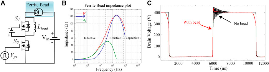
FIGURE 9. (A) Inductive load switching circuit with ferrite bead (B) Impedance graph of a low Q ferrite bead (Liu et al., 2018b) (C) Switching waveform of SiC MOSFET with and without ferrite bead (Kim et al., 2017).
As the characteristics of ferrite beads vary with load current, therefore, impedance vs load current curves should be referred to select the right ferrite bead. Figure 9C reveals the influence of ferrite bead on voltage oscillation of SiC MOSFET (Kim et al., 2017). Ferrite beads are effective for EMI reduction and at 15 MHz oscillation frequency, a noise reduction of 15 dB has been achieved in a SiC-based boost (Kim et al., 2017). By employing ferrite bead, 3.8% reduction in voltage overshoot and 78.45% reduction in oscillation duration of SiC MOSFET were achieved by Liu et al. (2018b). No matter how precisely parameters of ferrite are selected, a small amount of dc resistance is inevitable, which causes a slight increase in the conduction losses. Comprehensive design guidelines for ferrite beads can be found in Josifović et al. (2011), Josifovic et al. (2012), and Liu et al. (2018b).
To summarize, careful selection of a device with low package inductance and kelvin source can alleviate the oscillation. In addition, an optimized PCB layout offers reduced oscillation by diminishing the power loop and gate loop inductances. Increasing external gate resistance reduces the oscillation but slows down the switching speed leading to increased switching losses. Active gate driver can reduce the overshoots and cross-talk by controlling the di/dt and dv/dt, but increases the circuit cost and design complexity. The RC snubber method offers effective oscillation mitigation but slightly increases switching losses. Ferrite beads perform better to suppress high-frequency oscillations at the cost of slightly increased conduction loss. All oscillation mitigation methods have their pros and cons that are outlined in Table 1.
TABLE 1. Summary of methods for oscillation alleviation.
5 Methods to Mitigate Current Imbalance
5.1 Symmetrical Layout Method
The mismatch of parasitic parameters in the circuit is due to asymmetrical layout design (Graovac, 2009; Wang G. et al., 2014; Colmenares et al., 2015; Li et al., 2016; Haihong et al., 2017). This mismatch is the reason for the current imbalance which can be mitigated by realizing the symmetrical layout (Sadik et al., 2013). As mentioned earlier, the impact of Ls mismatch on current sharing is more prominent than that of Ld or Lg. Therefore, it is paramount to minimize discrepancy in Ls to reduce the current imbalance (La Mantia et al., 2017). Nevertheless, in many applications, due to layout constraints, it is extremely hard to achieve exactly symmetrical layout design. In such cases, a four-pin device that offers a kelvin connection can be adopted which provides a shorter path to the gate loop and bypass the Ls as shown in Figure 6B. Kelvin connection does not guarantee equal current distribution, yet it offers an opportunity to designers to achieve a better layout design, leading to improved current sharing.
This method can reduce the dynamic current imbalance and can provide a slight reduction in static current imbalance. For effective reduction of current imbalance, just realizing the symmetrical layout is not enough as it does not address the device mismatch. Generally, symmetrical layout design is a prerequisite for advanced current balancing methods. Besides, it does not offer increased switching speed, and energy losses cannot be minimized. Moreover, this method is difficult to adopt for more parallel-connected devices as the symmetrical layout is practically difficult to achieve for a higher number of devices.
5.2 Imbalance Mitigation via Source or Gate Resistors
Adjustment of gate or source resistor is a simple way to mitigate the current imbalance without adding any sensing or control circuit. One of the reasons for dynamic current imbalance is; a device with a lower Vth turns on earlier than the device with a higher Vth. There are two ways to reduce the effect of Vth mismatch using a gate resistor. First, the current imbalance can be suppressed by reducing the value of gate resistance if the same gate resistor is shared by the parallel-connected devices. Authors in Wang G. et al. (2014) achieved an effective reduction in current imbalance by reducing the gate resistance from 41 to 5.1 Ω at the cost of increased overshoot. The reason behind improved current sharing is; at a lower gate resistance, the switching speed increases and the effect of Vth mismatch become less significant. Another way is to add a suitable resistance only to the gate of the fast device with the lower Vth (Du et al., 2014). The fundamental principle behind adding the resistance is to delay the driving signal of the fast device (Du et al., 2014). Symmetrical layout is requisite for achieving promising results for both methods. Gate resistance adjustment can improve the dynamic current sharing and may offer a slight improvement in the current ratings. Nevertheless, it does not provide static current balancing since the Vth is the only parameter addressed in the strategy.
Employing additional source resistors in the parallel branches can suppress static current imbalance by reducing the RDSon mismatch. As the source resistors can only reduce the RDSon mismatch; therefore, no improvement in the dynamic current sharing can be attained and additional resistors cause extra power losses. Moreover, source resistors do not offer any reduction in voltage overshoot and gate oscillation (Zeng et al., 2020). Nonetheless, the cost, size and volume of gate and source resistance solutions are low and they can be employed for more than two devices.
5.3 Transfer Curve Screening Method
This method aims to reduce the device mismatch using the transfer curve screening method to select the devices with similar characteristics to improve the current distribution. As mentioned earlier, the dynamic current balance is influenced by the threshold voltage (Vth) and transconductance (gfs). Researchers in Fuji Electric (2016) screened the devices based on only Vth, and limited reduction in current imbalance was achieved since the effect of gfs was ignored (Lim et al., 2014; Wang G. et al., 2014; Kokosis et al., 2017). The scanning method adopted in Ke et al. (2018) takes into account both Vth and gfs for screening the devices. The gfs and Vth have the contrary effect on the current sharing as during turn-on transition, the device with larger gfs carries a more current, and the device with larger Vth carries a less current as can be seen in Eq. 1 (Ke et al., 2018).
In this method, first of all, the transfer curves of all devices are drawn and a particular procedure, as demonstrated in Figure 10A, is used to select the curves. Subsequently, selected curves are discretized and corresponding points of curves are compared under the equal drain current to get the Vgs difference. Under the equal drain current, x1 and x2 are abscissa values of the two curves that are used to measure the relative difference ε by using Eq. 5. The average of the relative difference (με), which represents the curve’s proximity, is then determined using Eq. 6, where n is the total number of sampling points and k is the serial number. The dominance of the transfer curve scanning method over the conventional counterpart is shown in Figure 10B, where among thirty tested devices, the devices with the lowest με (No. 20 and No. 27) accomplish better current sharing as compared to the devices with the smallest ΔVth (No. 15 and No. 17).
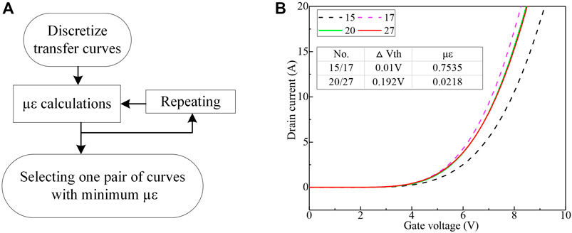
FIGURE 10. (A) Strategy for screening the transfer curves (B) transfer curves of devices no. 15, 17, 20 and 27 (Ke et al., 2018).
This method provides effective dynamic current sharing along with improved current rating. It can be used for more than two devices. Achieving a symmetrical layout is essential to adopt this method, as the effect of circuit discrepancies is avoided in the results by accomplishing a symmetrical layout. Nevertheless, the gate oscillation, voltage overshoot and energy losses cannot be reduced. This method does not provide increased switching speed, and static current imbalance cannot be minimized since RDSon is not considered. Furthermore, screening procedures are generally expensive and time-consuming (Graovac, 2009).
5.4 Active Current Balancing Method
An Active Current Balancing (ACB) technique has been presented in Xue et al. (2014b), where an active gate driver is used to accomplish equal current sharing among parallel-connected SiC MOSFETs. The current imbalance occurs due to several reasons and it is hard to anticipate until the circuit is fabricated. ACB technique diminishes the current imbalance regardless of its cause (Xue et al., 2013). This method immediately detects a current imbalance, using a differential current transformer (DTC) employed at the drain of the parallel-connected devices as shown in Figure 11B. The current imbalance is suppressed by using the current balancing controller that actively adjusts the gate current with gate delay (Xue et al., 2014b). The system block diagram is illustrated in Figure 11A. There are three subsystem blocks: current sensing block (CSB), current balancing controller (CBC), and active gate control (AGC). The CSB detects the current using DTC whereas CBC takes the DCT’s current difference signal and extracts the imbalance during turn-on and turn-off events. CBC generates the appropriate signal for AGC to eliminate the imbalance. Finally, the AGC uses the instructions from the CBC to adjust the gate signals using a variable gate delay (VGD) circuit during turn-on and turn-off events. In this way, three blocks work together to reduce the current imbalance.
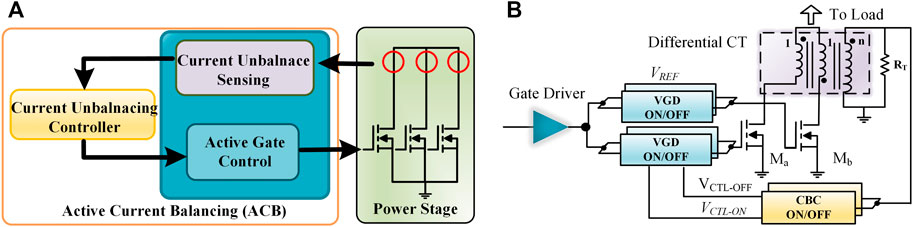
FIGURE 11. (A) Block diagram of the active current balancing (ACB) (B) Simplified circuit diagram of ACB (Xue et al., 2014b).
This method offers excellent dynamic current balancing and slightly improves the static current balance (Xue et al., 2014b). Moreover, this technique ensures small gate oscillation and low voltage overshoot. Although it does not improve the switching speed and no reduction in the energy losses was achieved. The complexity and cost of active current balancing are relatively higher due to additional sensing and control circuits. Besides, it does not ensure a small size and volume. In addition, the effective current balancing does not start from the first cycle; it takes more than ten cycles (Xue et al., 2014b). The high-bandwidth multi-channel current sensor requirement limits the adoption of this technique to two devices (Xue et al., 2014a). To address the current sensing issue, (Xue et al., 2014a) proposed a solution to measure the device’s current by using a PCB Rogowski coil current sensor. The design of the Rogowski coil is compact and planar along with high bandwidth, which allows accurate current measurement even with its dc component (Xue et al., 2014a). This method provides effective current sharing; however, the complexity of this method makes the integration tough.
5.5 Resistors and Coupled Power-Source Inductor Scheme
Current distribution can be improved by incorporating additional coupled power-source inductors and drive-source resistors as shown in Figure 12. This is an innovative passive current balancing solution that applied one gate driver to parallel-connected MOSFETs without requiring any sensors or feedback system. The circuit diagram of parallel-connected SiC MOSFETs is shown in Figure 12A along with the parasitic parameters. The authors assumed the layout to be exactly symmetrical and ignored the effect of all layout stray inductances including the common source inductance (Lcm) and the reduced diagram with compensating components as demonstrated in Figure 12B. The gate-source instance (Lk) assists current balancing without causing voltage stress. The resistor (Rk) enables voltage drop across the Lk. The loss impact of Rk in the gate loop is negligible as its size is extremely small compared with Lk. The power source inductor (Ls) also assists the current balancing but increases the voltage stress as well. To avoid the voltage stress caused by the Ls, they are negatively coupled as clarified in Figure 12B. The equivalent circuit diagram is shown in Figure 12C where coupled inductors are substituted as mutual inductance (Ms) and self-inductance (Ls). With the implementation of these additional components the power-source inductance gets amplified from Ls to Ls + Ms and gets diminished from Ls to Ls − Ms during differential-mode and common-mode path, respectively, enabling improved current distribution along with reduced voltage overshoot, ringing, and EMI noise. By using this passive solution, the peak current difference of parallel-connected SiC MOSFETs is reduced from 15 to 3% without any additional voltage stress or switching loss. In-depth analysis and equations to determine the values of different parameters such as mutual inductance, self-inductance and resistance are presented in Mao et al. (2017a). Based on this technique, new passive current balancing solutions can also be explored by replacing the Rk with an inductor or with the combination of resistor and inductor.
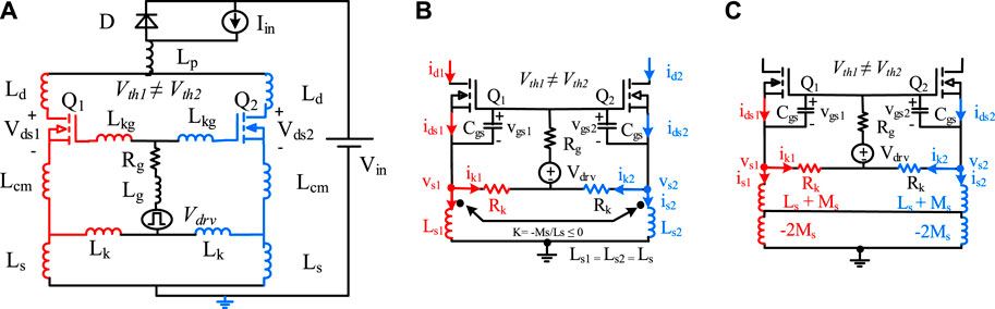
FIGURE 12. (A) Double pulse test (DPT) circuit of Parallel-connected MOSFETs with different Vth including circuit parasitic (B) Circuit diagram of parallel-connected SiC MOSFETs with additional components to balance the current distribution (C) Equivalent circuit diagram (Mao et al., 2017a) (Note: Rk = drive source resistor, Ms = mutual inductance, Ls = self-inductance, Ls1/Ls2 = power source inductors that are negatively coupled).
This innovative approach reduces the static and dynamic current imbalance and improves the overall current rating (Mao et al., 2017a). In addition, this method limits the gate oscillations, ringing, EMI issues and it is a low-cost solution. The effect of layout mismatch is excluded by realizing the symmetrical design in this method. Although the integration is not easy, this method can be implemented for more than two devices.
5.6 Differential Mode Choke Method
Inspired by the common-mode choke’s success to mitigate common mode current in high frequency switching mode power supplies, authors in Zeng et al. (2020) employed a differential mode (DM) choke to suppress current imbalance among parallel-connected SiC MOSFETs, as the nature of imbalance current is a kind of differential mode. The implementation of DM choke for the current balancing between parallel-connected SiC MOSFETs is demonstrated in Figure 13A. The basic operation of the DM choke is illustrated in Figures 13B,C, which shows that there is no magnetic flux density (Bc) in the case of balanced current (id1 = id2) and it is initiated by the imbalance current (id1 > id2) as shown in Figure 13C (Zeng et al., 2020). From the impedance perspective, imbalance current is shown in Eq. 7 where drain-source voltage is denoted by uds and Δid is the current difference. The impedances of parallel branches are represented by Z1 and Z2. The difference of current flows through the DM choke windings when the impedance of parallel branches is not equal. The current imbalance gets reduced by the induced voltage (vm) shown in Eq. 8 where Lm is magnetic inductance. During imbalance current suppression, one winding of DM choke senses energy (Pin = vmΔid) and transforms electric energy into magnetic. Meanwhile, the other winding energy produces energy (Pin = −vmΔid) and transforms magnetic energy into electrical energy (Zeng et al., 2020). In this way, DM choke uses magnetic flux as a medium to transmit current between parallel branches. In ideal conditions, it enables current imbalance suppression without any energy loss. Detailed guidelines to design the DM choke are presented in Zeng et al. (2020).
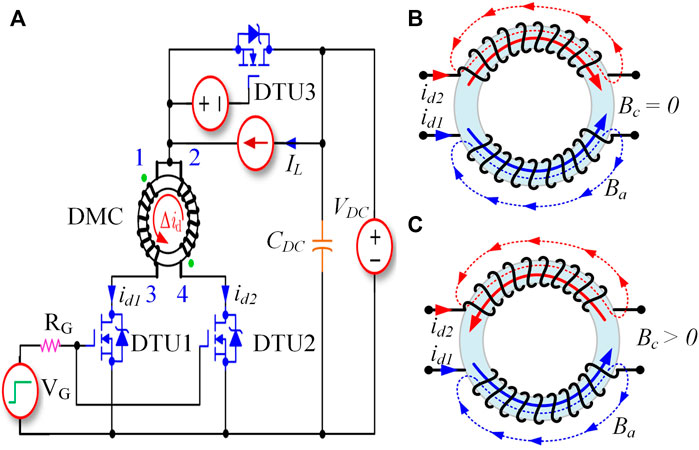
FIGURE 13. (A) Schematic diagram for imbalance current suppression by DM choke (B) Magnetic flux density (Bc) under balanced current id1 = id2 (C) Bc under imbalance current id1 > id2 (Zeng et al., 2020).
DM choke can effectively suppress both static and dynamic current imbalance even when different gate resistances are employed. In Zeng et al. (2020), parallel-connected SiC MOSFETs showed nearly identical current waveforms, including current rise and fall time and current peak value by employing DM choke. The DM choke improves the current ratings and reduces dv/dt which slightly diminishes the Vds overshoot. Though the switching losses slightly increase, the turn-on and turn-off losses (Eon and Eoff) of parallel-connected devices are nearly the same. It is recommended to use the bifilar winding for the DM choke since it minimizes leakage inductance and equivalent parallel capacitance (EPC) (Zeng et al., 2020). This method can be extended to more than two devices. Mechanisms of interaction between DM choke and SiC MOSFETs need further research to explore cross-talk, short-circuit, etc. (Zeng et al., 2020). The cost and design effort of the DM choke method are lower than ACB because the former one does not require any complex control scheme and feedback. A comparison of the different methods is presented in Table 2.
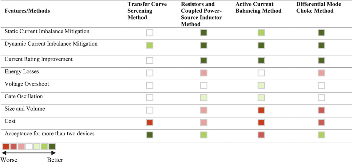
TABLE 2. Evaluation of advanced current imbalance mitigation methods.
6 Stray Parameter Extraction Methods
The stray parameters in the circuit are the reason behind oscillations and also impact the current distribution. Their accurate estimation can provide necessary guidance to analyze and mitigate the oscillation and current imbalance. In the literature, simulation and experimental based studies have been carried out to extract the stray inductance. In simulation-based studies, different software like FastHenry, ANSYS Q3D, FastCap, finite-element analysis (FEA) have been reported to extract the stray inductance (Lianghua et al., 2006; Chen et al., 2009; Fu et al., 2013; Liu et al., 2014). Software-based extraction is complex and demands precise molding; however, complete information of structure, material, dimensions and interconnections of commercialized devices is usually not available. Besides, it is time-consuming and convergence is poor for complex packages. On the other hand, experimental methods are relatively simple and can be divided into time domain and frequency domain methods. Time-domain methods (Ariga et al., 2012; Li S. et al., 2014; Kexin et al., 2014) calculate the stray inductance by measuring the voltage U, rate of change of current di/dt, and then using the expression U = L(di/dt). The accuracy of time-domain methods highly depends on the measuring probe’s sensitivity and data processing technique. In addition, they extract the total inductance of the device and the power loop and individual inductances cannot be extracted; though, (Umetani et al., 2017) suggested a way to calculate common source inductance. In high frequency/power applications, extraction of equivalent series inductance (ESL) of a dc-link capacitor, internal package inductance of device and stray inductance of busbar is crucial to anticipate and optimize the switching performance. Frequency domain methods reported in Sadik et al. (2016) and Liu et al. (2020) overcame some limitations of the time domain methods by exploiting the relationship of power loop parameters with underdamped frequency to calculate the stray inductance. Nonetheless, the discussed time domain and frequency domain methods only extract the stray inductance and the contribution of stray capacitance and package inductance remained obscure. New methods have been reported in Wang et al. (2020), Hu et al. (2021b), and Hu et al. (2021a) which can extract both stray inductance and stray capacitance by leveraging the parasitic ringing of the device and the impact on DC-link is explored in Krishna Moorthy et al. (2020), Meng et al. (2020), and Liang et al. (2021). Package inductance extraction of discrete devices is investigated in Liu et al. (2014), Liu et al. (2018a), and Xie et al. (2019) where two port extraction strategy outperforms the single port method (Liu et al., 2018a). Other researches have explored the techniques to minimize the stray parameters and in-depth investigation has been provided in Shtargot et al. (2012), Reusch and Strydom (2014), Meng et al. (2021), and Pace et al. (2021). Research on the extraction methods is still limited especially for extracting ESL of a dc-link capacitor and package inductance of discrete devices, bringing new research opportunities for young researchers.
7 Conclusion
Discrete package offers a cost-effective solution with design flexibility and scalability. Severe switching oscillations and limited current ratings are the main challenges faced by discrete packages. This paper organized the oscillations with respect to voltage and their underlying oscillations mechanisms are presented. Current distribution among parallel-connected discrete devices is categorized into static current imbalance and dynamic current imbalance. In addition, the root causes and negative impacts of the current imbalance are discussed. Furthermore, newly reported stray parameter extraction methods are also reviewed. Finally, state-of-the-art solutions to mitigate the oscillations and current imbalance are summarized. To fully leverage the potential of the discrete WBG devices, guidelines are given below:
1) Select a package with kelvin source. Among kelvin source packages, TO-263-7 offers low package inductance and TO-247-4 offers relatively high current ratings.
2) During layout design, the power loop and drive loop inductance should be kept as small as possible. A double layout design method can be adopted which can reduce voltage overshot by 8.3% and increase efficiency by 0.6% (Wang K. et al., 2017).
3) While selecting the gate resistor, a trade-off should be made between switching oscillations and switching losses. Careful selection of gate resistor should be made in such a way that it keeps the switching oscillations within safe limits without a substantial increase in the switching losses.
4) Compared to the gate resistor technique, the RC snubber has a minor increase in switching losses. Active gate driver can reduce the voltage overshoot and cross-talk by controlling the di/dt and dv/dt, but increases the circuit cost and design complexity. Ferrite bead is a good choice to mitigate high-frequency oscillation though it cost a slight increase in conduction losses. The benefits and drawbacks of different methods are summarized in Table 1.
5) To increase the current ratings, discrete devices are used in parallel. The devices with a minimum difference of RDSon and Vth should be selected using the screening process to achieve better performance. Yet the benefits of the screening method should be weighed against the cost.
6) In parallel design layout, matching of common source inductance (Ls) is paramount to reduce the dynamic current imbalance and kelvin source packages can assist the design.
7) The reduction of gate resistance can improve the dynamic current sharing but does not improve the static current sharing. Implementation of additional source resistors can mitigate the static current imbalance but increase the energy losses and no improvement in the dynamic current sharing is obtainable. The active current balancing method is effective for mitigating both static and dynamic current imbalance, ensuring small gate oscillation and low voltage overshoot; however, it is hard to adopt for a higher number of devices. Among current sharing solutions, coupled power-source inductor method and differential mode choke method offer excellent current sharing features. The comparison of advanced methods is presented in Table 2.
8) Newly reported stray parameters extraction methods should be leveraged since they provide accurate estimation which can offer necessary guidance to analyze and design innovative solutions to mitigate the switching oscillation and current imbalance.
This work will assist the readers in the following ways:
1) It provides clear comprehension of the oscillation and current imbalance challenges associated with discrete devices along with their underlying mechanisms.
2) It offers the clear recognition of exciting solutions including their benefits and drawbacks.
3) To fully unleash the potential of discrete devices, guidelines are also provided.
4) The solutions are the guidelines illustrated in this survey can easily be extended to module packages and silicon-based devices.
5) The limited research on stray parameters extraction methods is also pointed out which reveals new research opportunities for young researchers.
6) The in-depth and comprehensive outline of challenges and their root causes provided in this work can stimulate the readers to come up with new solutions.
Research on discrete packages is still evolving and there will be methods in the future.
Author Contributions
MT and SH conceptualized and performed the review process. MT was responsible for the main writing of the paper, while SH was responsible for the revision of the paper. XH provided the ideas and revised the manuscript based on his extensive knowledge and experience in power electronics. All authors contributed to the article and approved the submitted version.
Funding
This work was supported by National Natural Science Foundation of China (52177199).
Conflict of Interest
The authors declare that the research was conducted in the absence of any commercial or financial relationships that could be construed as a potential conflict of interest.
Publisher’s Note
All claims expressed in this article are solely those of the authors and do not necessarily represent those of their affiliated organizations, or those of the publisher, the editors and the reviewers. Any product that may be evaluated in this article, or claim that may be made by its manufacturer, is not guaranteed or endorsed by the publisher.
References
Abou-Alfotouh, A. M., Radun, A. V., Chang, H.-R., and Winterhalter, C. (2006). A 1-MHz Hard-Switched Silicon Carbide DC-DC Converter. IEEE Trans. Power Electron. 21, 880–889. doi:10.1109/tpel.2006.876891
Adamowicz, M., Giziewski, S., Pietryka, J., Rutkowski, M., and Krzeminski, Z. (2011). “Evaluation of SiC JFETs and SiC Schottky Diodes for Wind Generation Systems,” in 2011 IEEE International Symposium on Industrial Electronics, Gdansk, Poland, 27-30 June 2011 (IEEE), 269–276. doi:10.1109/ISIE.2011.5984169
Ahmed, M. R., Todd, R., and Forsyth, A. J. (2017). Predicting SiC MOSFET Behavior under Hard-Switching, Soft-Switching, and False Turn-On Conditions. IEEE Trans. Ind. Electron. 64, 9001–9011. doi:10.1109/TIE.2017.2721882
Aikawa, K., Shiida, T., Matsumoto, R., Umetani, K., and Hiraki, E. (2017). “Measurement of the Common Source Inductance of Typical Switching Device Packages,” in 2017 IEEE 3rd International Future Energy Electronics Conference and ECCE Asia (IFEEC 2017 - ECCE Asia), Kaohsiung, Taiwan, 3-7 June 2017 (IEEE), 1172–1177. doi:10.1109/IFEEC.2017.7992207
Alatise, O., Parker-Allotey, N.-A., Hamilton, D., and Mawby, P. (2012). The Impact of Parasitic Inductance on the Performance of Silicon-Carbide Schottky Barrier Diodes. IEEE Trans. Power Electron. 27, 3826–3833. doi:10.1109/tpel.2012.2183390
Alexakis, P., Alatise, O., Ran, L., and Mawby, P. (2013). “Modeling Power Converters Using Hard Switched Silicon Carbide MOSFETs and Schottky Barrier Diodes,” in 2013 15th European Conference on Power Electronics and Applications (EPE), Lille, France, 2-6 Sept. 2013 (IEEE), 1–9. doi:10.1109/epe.2013.6631758
Alizadeh, R., and Alan Mantooth, H. (2021). A Review of Architectural Design and System Compatibility of Power Modules and Their Impacts on Power Electronics Systems. IEEE Trans. Power Electron. 36, 11631–11646. doi:10.1109/TPEL.2021.3068760
Ando, M., and Wada, K. (2017). Design of Acceptable Stray Inductance Based on Scaling Method for Power Electronics Circuits. IEEE J. Emerg. Sel. Top. Power Electron. 5, 568–575. doi:10.1109/JESTPE.2016.2638019
Anthon, A., Hernandez, J. C., Zhang, Z., and Andersen, M. A. E. (2014). “Switching Investigations on a SiC MOSFET in a TO-247 Package,” in IECON 2014-40th Annual Conference of the IEEE Industrial Electronics Society, Dallas, TX, USA, 29 Oct.-1 Nov. 2014 (IEEE), 1854–1860. doi:10.1109/iecon.2014.7048754
Ariga, Z.-N., Wada, K., and Shimizu, T. (2012). TDR Measurement Method for Voltage-dependent Capacitance of Power Devices and Components. IEEE Trans. Power Electron. 27, 3444–3451. doi:10.1109/TPEL.2011.2181956
Arribas, A. P., Shang, F., Krishnamurthy, M., and Shenai, K. (2015). Simple and Accurate Circuit Simulation Model for SiC Power MOSFETs. IEEE Trans. Electron. Devices 62, 449–457. doi:10.1109/TED.2014.2384277
Azizouglu, B. T., and Karaca, H. (2014). Investigating a MOSFET Driver (Buffer) Circuit Transition Ringings Using an Analytical Model. IEEE Trans. Power Electron. 30, 5058–5066.
Bertelshofer, T., Denk, M., and Bakran, M.-M. (2019). “Design Study and Prototype of 150 kW Inverter with Discrete SiC MOSFETs,” in PCIM Europe 2019; International Exhibition and Conference for Power Electronics, Intelligent Motion, Renewable Energy and Energy Management, Nuremberg, Germany, 7-9 May 2019 (Nuremberg: VDE), 1–8.
Camacho, A. P., Sala, V., Ghorbani, H., and Martinez, J. L. R. (2017). A Novel Active Gate Driver for Improving SiC MOSFET Switching Trajectory. IEEE Trans. Ind. Electron. 64, 9032–9042. doi:10.1109/TIE.2017.2719603
Cao, J., Zhou, Z.-k., Wang, Z., Tang, H., and Zhang, B. (2021). Design Techniques of Sub-ns Level Shifters with Ultrahigh dV/dt Immunity for Various Wide-Bandgap Applications. IEEE Trans. Power Electron. 36, 10447–10460. doi:10.1109/TPEL.2021.3061715
Chen, C., Luo, F., and Kang, Y. (2017). A Review of SiC Power Module Packaging: Layout, Material System and Integration. Cpss Tpea 2, 170–186. doi:10.24295/cpsstpea.2017.00017
Chen, J., Luo, Q., Huang, J., He, Q., Sun, P., and Du, X. (2020). Analysis and Design of an RC Snubber Circuit to Suppress False Triggering Oscillation for GaN Devices in Half-Bridge Circuits. IEEE Trans. POWER Electron. 35, 2690–2704. doi:10.1109/TPEL.2019.2927486
Chen, J., Luo, Q., Wei, Y., Zhang, X., and Du, X. (2021). The Sustained Oscillation Modeling and its Quantitative Suppression Methodology for GaN Devices. IEEE Trans. Power Electron. 36 (7), 7927–7941.
Chen, Z., and Amaro, I. (2012). “Optimizing Low Side Gate Resistance for Damping Phase Node Ringing of Synchronous Buck Converter,” in 2012 IEEE Energy Conversion Congress and Exposition (ECCE), Raleigh, NC, USA, 15-20 Sept. 2012 (IEEE), 1827–1832. doi:10.1109/ECCE.2012.6342590
Chen, Z. (2014). “An Inductive-Switching Loss Model Accounting for Source Inductance and Switching Loop Inductance,” in 2014 IEEE Applied Power Electronics Conference and Exposition-APEC 2014, Fort Worth, TX, USA, 16-20 March 2014 (IEEE), 497–504. doi:10.1109/apec.2014.6803355
Chen, Z., Boroyevich, D., and Burgos, R. (2010). “Experimental Parametric Study of the Parasitic Inductance Influence on MOSFET Switching Characteristics,” in The 2010 International Power Electronics Conference-ECCE ASIA-, Sapporo, Japan, 21-24 June 2010 (IEEE), 164–169. doi:10.1109/ipec.2010.5543851
Chen, Z., Boroyevich, D., Mattavelli, P., and Ngo, K. (2013a). “A Frequency-Domain Study on the Effect of DC-link Decoupling Capacitors,” in 2013 IEEE Energy Conversion Congress and Exposition, Denver, CO, USA, 15-19 Sept. 2013 (IEEE), 1886–1893. doi:10.1109/ECCE.2013.6646938
Chen, Z., Burgos, R., Boroyevich, D., Wang, F., and Leslie, S. (2009). “Modeling and Simulation of 2 kV 50 A SiC MOSFET/JBS Power Modules,” in 2009 IEEE Electric Ship Technologies Symposium, Baltimore, MD, USA, 20-22 April 2009 (IEEE), 393–399. doi:10.1109/ESTS.2009.4906542
Chen, Z. (2009). Characterization and Modeling of High-Switching-Speed Behavior of SiC Active Devices. Doctoral Thesis. (Blacksburg, Virginia: Virginia Tech).
Chen, Z., Danilovic, M., Boroyevich, D., and Shen, Z. (2011). “Modularized Design Consideration of a General-Purpose, High-Speed Phase-Leg PEBB Based on SiC MOSFETs,” in Proceedings of the 2011 14th European Conference on Power Electronics and Applications, Birmingham, UK, 30 Aug.-1 Sept. 2011 (IEEE), 1–10.
Chen, Z., Liu, S., and Shi, L. (2013b). A Soft Switching Full Bridge Converter with Reduced Parasitic Oscillation in a Wide Load Range. IEEE Trans. Power Electron. 29, 801–811.
Chen, Z., Liu, S., Wang, Y., and Shi, L. (2013c). “Soft Switching Full-Bridge Converter with a Wide ZVS Range and Reduced Parasitic Oscillation,” in 2013 IEEE Energy Conversion Congress and Exposition, Denver, CO, USA, 15-19 Sept. 2013 (IEEE), 5440–5447. doi:10.1109/ECCE.2013.6647439
Chen, Z., Yao, Y., Boroyevich, D., Ngo, K. D. T., Mattavelli, P., and Rajashekara, K. (2014). A 1200-V, 60-A SiC MOSFET Multichip Phase-Leg Module for High-Temperature, High-Frequency Applications. IEEE Trans. Power Electron. 29, 2307–2320. doi:10.1109/TPEL.2013.2283245
Chuai, G., Wang, J., Yuan, X., Lai, B., and Zhang, Q. (2019). “Design and Parasitic Parameters Analysis of A LCC Resonant Inverter Using SiC MOSFET,” in 2019 22nd International Conference on Electrical Machines and Systems (ICEMS), Harbin, China, 11-14 Aug. 2019 (IEEE), 1–6. doi:10.1109/ICEMS.2019.8921862
Colmenares, J., Peftitsis, D., Rabkowski, J., Sadik, D.-P., Tolstoy, G., and Nee, H.-P. (2015). High-Efficiency 312-kVA Three-phase Inverter Using Parallel Connection of Silicon Carbide MOSFET Power Modules. IEEE Trans. Ind. Applicat. 51, 4664–4676. doi:10.1109/TIA.2015.2456422
CREE (2011). Application Considerations for Silicon Carbide MOSFETs. 1–3. Available at:http://www.cree.com/∼/media/Files/Cree/Power/Application Notes/CPWRAN08.pdf.
CREE (2021b). Sic-mosfets. Available at:https://www.wolfspeed.com/power/products/sic-mosfets (Accessed September 10, 2021).
Ding, X., Du, M., Duan, C., Guo, H., Xiong, R., Xu, J., et al. (2017). Analytical and Experimental Evaluation of SiC-Inverter Nonlinearities for Traction Drives Used in Electric Vehicles. IEEE Trans. Veh. Technol. 67, 146–159.
Dodge, J. (2004). Eliminating Parasitic Oscillation between Parallel MOSFETs. Bend, United States: Adv. Power Technol. Appl. note APT-0402 Rev A.
Dong, Z., Wu, X., Sheng, K., and Zhang, J. (2015). “Impact of Common Source Inductance on Switching Loss of SiC MOSFET,” in 2015 IEEE 2nd International Future Energy Electronics Conference (IFEEC), Taipei, Taiwan, 1-4 Nov. 2015 (IEEE), 1–5. doi:10.1109/IFEEC.2015.7361607
Du, M., Ding, X., Guo, H., and Liang, J. (2014). “Transient Unbalanced Current Analysis and Suppression for Parallel-Connected Silicon Carbide MOSFETs,” in IEEE Transp. Electrif. Conf. Expo, ITEC Asia-Pacific 2014 - Conf. Proc., Beijing, China, 31 Aug.-3 Sept. 2014 (IEEE), 2–5. doi:10.1109/ITEC-AP.2014.6941230
Dymond, H. C. P., Wang, J., Liu, D., Dalton, J. J. O., McNeill, N., Pamunuwa, D., et al. (2018). A 6.7-GHz Active Gate Driver for GaN FETs to Combat Overshoot, Ringing, and EMI. IEEE Trans. POWER Electron. 33, 581–594. doi:10.1109/TPEL.2017.2669879
Elbanhawy, A. (2005). Limiting Cross-Conduction Current in Synchronous Buck Converter Designs. San Jose, CA, USA: Fairchild Semicond. Appl. Note AN-7019.
Fan, D., Liang, Z., Hu, S., Yang, H., Gu, X., and He, X. (2016). “Principle and Implementation of the Shoot-Through Current Reconstruction Using Combined Current Sensing in the Quasi-Z-Source Inverter,” in 2016 IEEE Vehicle Power and Propulsion Conference (VPPC), Hangzhou, China, 17-20 Oct. 2016 (IEEE), 1–5. doi:10.1109/VPPC.2016.7791755
Fang, Z., Jiang, D., Shen, Z., and Qu, R. (2017). “Impact of Application of SiC Devices in Motor Drive on EMI,” in 2017 IEEE Applied Power Electronics Conference and Exposition (APEC), Tampa, FL, USA, 26-30 March 2017 (IEEE), 652–658. doi:10.1109/APEC.2017.7930763
Fu, R., Grekov, A., Peng, K., and Santi, E. (20132013). “Parasitic Modeling for Accurate Inductive Switching Simulation of Converters Using SiC Devices,” in IEEE Energ. Convers. Congress Exposition, Denver, United States, 1259–1265. doi:10.1109/ECCE.2013.6646849
Fujihira, T., Yamada, T., Minoya, Y., Kobayashi, T., Niimura, Y., Kuboyama, T., et al. (2008). “New Oscillation Circuit Discovered in Switching-Mode Power Supplies,” in 2008 20th International Symposium on Power Semiconductor Devices and IC’s, Orlando, FL, USA, 18-22 May 2008 (IEEE), 193–196. doi:10.1109/ispsd.2008.4538931
Gafford, J., Mazzola, M., Lemmon, A., and Parker, C. (2013). “Stable High dV/dt Switching of SiC JFETs Using Simple Drive Methods,” in 2013 TWENTY-EIGHTH ANNUAL IEEE APPLIED POWER ELECTRONICS CONFERENCE AND EXPOSITION (APEC 2013) Annual IEEE Applied Power Electronics Conference and Exposition (APEC)., Long Beach, CA, USA, 17-21 March 2013 (IEEE), 2450–2452. doi:10.1109/apec.2013.6520639
Gamand, F., Li, M. D., and Gaquiere, C. (2012). A 10-MHz GaN HEMT DC/DC Boost Converter for Power Amplifier Applications. IEEE Trans. Circuits Syst. 59, 776–779. doi:10.1109/TCSII.2012.2228397
Gao, F., Zhou, Q., Wang, P., and Zhang, C. (2018). A Gate Driver of SiC MOSFET for Suppressing the Negative Voltage Spikes in a Bridge Circuit. IEEE Trans. POWER Electron. 33, 2339–2353. doi:10.1109/TPEL.2017.2690938
Githiari, A. N., and Palmer, P. R. (1998). Analysis of IGBT Modules Connected in Series. IEE Proc. Circuits Devices Syst. 145, 354–360. doi:10.1049/ip-cds:19982123
Guichao Hua, G., Ching-Shan Leu, C.-S., Yimin Jiang, Y., and Lee, F. C. Y. (1994). Novel Zero-Voltage-Transition PWM Converters. IEEE Trans. Power Electron. 9, 213–219. doi:10.1109/63.286814
Haihong, Q., Ying, Z., Ziyue, Z., Dan, W., and Shishan, W. (2017). Silicon Carbide MOSFETs, 556–561.
Hou, F., Wang, W., Cao, L., Li, J., Su, M., Lin, T., et al. (2020). Review of Packaging Schemes for Power Module. IEEE J. Emerg. Sel. Top. Power Electron. 8, 223–238. doi:10.1109/jestpe.2019.2947645
Hu, S., Wang, M., Liang, Z., and He, X. (2021a). A Frequency-Based Stray Parameter Extraction Method Based on Oscillation in SiC MOSFET Dynamics. IEEE Trans. Power Electron. 36, 6153–6157. doi:10.1109/TPEL.2020.3033801
Hu, S., Wang, M., Liang, Z., and He, X. (2021b). Method for Extracting Equivalent Series Inductance of Film Capacitor Based on Switch Transient Frequency Information, Involves Calculating Internal Equivalent Series Inductance of To-Be-Tested Capacitor According to Oscillation Frequency. Chinese Patent CN112433097-A., Hangzhou.
Hu, Y., and Shao, J. (2021). “Parallel Operation of SiC MOSFETs,” in PCIM Europe Digital Days 2021; International Exhibition and Conference for Power Electronics, Intelligent Motion (Renewable Energy and Energy Management), 1–5.
Huang, X., Du, W., Lee, F. C., Li, Q., and Zhang, W. (2017). Avoiding Divergent Oscillation of a Cascode GaN Device under High-Current Turn-Off Condition. IEEE Trans. POWER Electron. 32, 593–601. doi:10.1109/tpel.2016.2532799
Hughes, B., Lazar, J., Hulsey, S., Zehnder, D., Matic, D., and Boutros, K. (2012). “GaN HFET Switching Characteristics at 350V/20A and Synchronous Boost Converter Performance at 1MHz,” in 2012 TWENTY-SEVENTH ANNUAL IEEE APPLIED POWER ELECTRONICS CONFERENCE AND EXPOSITION (APEC) Annual IEEE Applied Power Electronics Conference and Exposition (APEC)., Orlando, FL, USA, 5-9 Feb. 2012 (IEEE), 2506–2508. doi:10.1109/apec.2012.6166174
Idir, N., Bausiere, R., and Franchaud, J. J. (2006). Active gate voltage control of turn-on di/dt and turn-off dv/dt in insulated gate transistors. IEEE Trans. Power Electron. 21, 849–855. doi:10.1109/tpel.2007.876895
Infineon (2021a). Silicon Carbide Discretes. Available at: https://www.infineon.com/cms/en/product/power/mosfet/silicon-carbide/discretes/(Accessed September 10, 2021).
Infineon (2021b). TO-247plus. Available at: https://www.infineon.com/cms/en/product/power/igbt/igbt-discretes/latest-discrete-packages/to-247plus/(Accessed September 10, 2021).
Infineon (2021c). What SiC Package Should I Choose – a Discrete or Module Package. Available at: https://www.infineon.com/cms/en/blog/What-SiC-package-should-I-choose-a-discrete-or-module-package (Accessed September 10, 2021).
Ishibashi, H., Nishigaki, A., Umegami, H., Martinez, W., and Yamamoto, M. (2015). “An Analysis of False Turn-On Mechanism on High-Frequency Power Devices,” in 2015 IEEE ENERGY CONVERSION CONGRESS AND EXPOSITION (ECCE) IEEE Energy Conversion Congress and Exposition, Montreal, QC, Canada, 20-24 Sept. 2015 (IEEE), 2247–2253. doi:10.1109/ECCE.2015.7309976
Jahdi, S., Alatise, O., Gonzalez, J. O., Ran, L., and Mawby, P. (2015). “Comparative Analysis of False Turn-ON in Silicon Bipolar and SiC Unipolar Power Devices,” in 2015 IEEE ENERGY CONVERSION CONGRESS AND EXPOSITION (ECCE) IEEE Energy Conversion Congress and Exposition, Montreal, QC, Canada, 20-24 Sept. 2015 (IEEE), 2239–2246.
Jahns, T. M., and Dai, H. (2017). The Past, Present, and Future of Power Electronics Integration Technology in Motor Drives. Cpss Tpea 2, 197–216. doi:10.24295/cpsstpea.2017.00019
Ji, S., Zhang, Z., and Wang, F. (2017). Overview of High Voltage SiC Power Semiconductor Devices: Development and Application. Trans. Electr. Mach. Syst. 1, 254–264. doi:10.23919/tems.2017.8086104
Jih-Sheng Lai, J.-S. (1997). Resonant Snubber-Based Soft-Switching Inverters for Electric Propulsion Drives. IEEE Trans. Ind. Electron. 44, 71–80. doi:10.1109/41.557501
Joko, M., Goto, A., Hasegawa, M., Miyahara, S., and Murakami, H. (2015). “Snubber Circuit to Suppress the Voltage Ringing for SiC Device,” in Proceedings of PCIM Europe 2015; International Exhibition and Conference for Power Electronics, Intelligent Motion, Renewable Energy and Energy Management, Nuremberg, Germany, 19-20 May 2015 (Nuremberg: VDE), 1–6.
Jones, E. A., Wang, F. F., and Costinett, D. (2016). Review of Commercial GaN Power Devices and GaN-Based Converter Design Challenges. IEEE J. Emerg. Sel. Top. Power Electron. 4, 707–719. doi:10.1109/JESTPE.2016.2582685
Josifovic, I., Popovic-Gerber, J., and Ferreira, J. A. (2012). Improving SiC JFET Switching Behavior under Influence of Circuit Parasitics. IEEE Trans. POWER Electron. 27, 3843–3854. doi:10.1109/TPEL.2012.2185951
Josifović, I., Popović-Gerber, J., and Ferreira, J. A. (2011). “SiC JFET Switching Behavior in a Drive Inverter under Influence of Circuit Parasitics,” in 8th International Conference on Power Electronics-ECCE Asia, Jeju, Korea (South), 30 May-3 June 2011 (IEEE), 087–1094. doi:10.1109/icpe.2011.5944659
Jun Wang, J., Xiaohu Zhou, X., Jun Li, J., Tiefu Zhao, T., Huang, A. Q., Callanan, R., et al. (2009). 10-kV SiC MOSFET-Based Boost Converter. IEEE Trans. Ind. Applicat. 45, 2056–2063. doi:10.1109/TIA.2009.2031915
Kassakian, J. G., and Lau, D. (1984). An Analysis and Experimental Verification of Parasitic Oscillations in Parralleled Power MOSFET's. IEEE Trans. Electron. Devices 31, 959–963. doi:10.1109/t-ed.1984.21637
Ke, J., Zhao, Z., Sun, P., Huang, H., Abuogo, J., and Cui, X. (2018). “New Screening Method for Improving Transient Current Sharing of Paralleled SiC MOSFETs,” in 2018 Int. Power Electron. Conf. IPEC-Niigata - ECCE Asia 2018, Niigata, Japan, 20-24 May 2018 (IEEE), 1125–1130. doi:10.23919/IPEC.2018.8507893
Kelley, R., Rees, F., and Schwob, D. (2009). “Optimized Gate Driver for Enhancement-Mode SiC JFET,” in Proc. of Power Conversion Intelligent Motion PCIM, 2009, Nuremberg, Germany, 12-14 May 2009.
Kexin, W., Mingxing, D., Linlin, X., and Jian, L. (2014). Study of Bonding Wire Failure Effects on External Measurable Signals of IGBT Module. IEEE Trans. Device Mater. Relib. 14, 83–89. doi:10.1109/TDMR.2012.2200485
Khanna, R., Amrhein, A., Stanchina, W., Reed, G., and Mao, Z.-H. (2013). “An Analytical Model for Evaluating the Influence of Device Parasitics on Cdv/dt Induced False Turn-On in SiC MOSFETs,” in 2013 TWENTY-EIGHTH ANNUAL IEEE APPLIED POWER ELECTRONICS CONFERENCE AND EXPOSITION (APEC 2013) Annual IEEE Applied Power Electronics Conference and Exposition (APEC)., Long Beach, CA, USA, 17-21 March 2013 (IEEE), 518–525. doi:10.1109/apec.2013.6520259
Kim, T., Feng, D., Jang, M., and Agelidis, V. G. (2017). Common Mode Noise Analysis for Cascaded Boost Converter with Silicon Carbide Devices. IEEE Trans. Power Electron. 32, 1917–1926. doi:10.1109/TPEL.2016.2569424
Kokosis, S. G., Andreadis, I. E., Kampitsis, G. E., Pachos, P., and Manias, S. (2017). Forced Current Balancing of Parallel-Connected SiC JFETs during Forward and Reverse Conduction Mode. IEEE Trans. Power Electron. 32, 1400–1410. doi:10.1109/TPEL.2016.2553133
Krishna Moorthy, R. S., Aberg, B., Olimmah, M., Yang, L., Rahman, D., Lemmon, A. N., et al. (2020). Estimation, Minimization, and Validation of Commutation Loop Inductance for a 135-kW SiC EV Traction Inverter. IEEE J. Emerg. Sel. Top. Power Electron. 8, 286–297. doi:10.1109/JESTPE.2019.2952884
La Mantia, S., Abbatelli, L., Brusca, C., Melito, M., and Nania, M. (2017). “Design Rules for Paralleling of Silicon Carbide Power MOSFETs,” in PCIM Eur. 2017 - Int. Exhib. Conf. Power Electron. Intell. Motion, Renew. Energy Energy Manag, Nuremberg, Germany, 16-18 May 2017 (Nuremberg: VDE), 16–18. doi:10.1109/SBMicro.2017.7990864
Lee, H., Smet, V., and Tummala, R. (2020). A Review of SiC Power Module Packaging Technologies: Challenges, Advances, and Emerging Issues. IEEE J. Emerg. Sel. Top. Power Electron. 8, 239–255. doi:10.1109/jestpe.2019.2951801
Lemmon, A., Banerjee, S., Matocha, K., and Gant, L. (2016). “Analysis of Packaging Impedance on Performance of SiC MOSFETs,” in PCIM Eur. 2016; Int. Exhib. Conf. Power Electron. Intell. Motion, Renew. Energy Energy Manag., Nuremberg, Germany, 10-12 May 2016 (Nuremberg: VDE), 984–991.
Lemmon, A., Graves, R., and Gafford, J. (2015). “Evaluation of 1.2 kV, 100A SiC Modules for High-Frequency, High-Temperature Applications,” in 2015 THIRTIETH ANNUAL IEEE APPLIED POWER ELECTRONICS CONFERENCE AND EXPOSITION (APEC 2015) Annual IEEE Applied Power Electronics Conference and Exposition (APEC)., Charlotte, NC, USA, 15-19 March 2015 (IEEE), 789–793. doi:10.1109/apec.2015.7104439
Lemmon, A., Mazzola, M., Gafford, J., and Parker, C. (2014). Instability in Half-Bridge Circuits Switched with Wide Band-Gap Transistors. IEEE Trans. Power Electron. 29, 2380–2392. doi:10.1109/TPEL.2013.2273275
Lemmon, A., Mazzola, M., Gafford, J., and Parker, C. (2013). Stability Considerations for Silicon Carbide Field-Effect Transistors. IEEE Trans. POWER Electron. 28, 4453–4459. doi:10.1109/TPEL.2012.2226473
Letellier, A., Dubois, M. R., Trovao, J. P. F., and Maher, H. (2019). Calculation of Printed Circuit Board Power-Loop Stray Inductance in GaN or High di/dt Applications. IEEE Trans. Power Electron. 34, 612–623. doi:10.1109/TPEL.2018.2826920
Li, C., Lu, Z., Chen, Y., Li, C., Luo, H., Li, W., et al. (2020a). High Off-State Impedance Gate Driver of SiC MOSFETs for Crosstalk Voltage Elimination Considering Common-Source Inductance. IEEE Trans. Power Electron. 35, 2999–3011. doi:10.1109/TPEL.2019.2932263
Li, H., and Munk-nielsen, S. (2014). “Challenges in Switching SiC MOSFET without Ringing Oscillation Mechanism of Switching SiC MOSFET,” in PCIM Europe 2014; International Exhibition and Conference for Power Electronics, Intelligent Motion, Renewable Energy and Energy Management, Nuremberg, Germany, 20-22 May 2014 (Nuremberg: VDE), 22–20.
Li, H., and Munk-Nielsen, S. (2014a). “Detail Study of SiC MOSFET Switching Characteristics,” in 2014 IEEE 5th International Symposium on Power Electronics for Distributed Generation Systems (PEDG) (IEEE), Galway, Ireland, 24-27 June 2014 (IEEE), 1–5. doi:10.1109/pedg.2014.6878691
Li, H., Munk-Nielsen, S., Pham, C., and Beczkowski, S. (2014a). “Circuit Mismatch Influence on Performance of Paralleling Silicon Carbide MOSFETs,” in 2014 16th Eur. Conf. Power Electron. Appl. EPE-ECCE Eur. 2014, Lappeenranta, Finland, 26-28 Aug. 2014 (IEEE). doi:10.1109/EPE.2014.6910835
Li, H., Munk-Nielsen, S., Wang, X., Maheshwari, R., Beczkowski, S., Uhrenfeldt, C., et al. (2016). Influences of Device and Circuit Mismatches on Paralleling Silicon Carbide MOSFETs. IEEE Trans. Power Electron. 31, 621–634. doi:10.1109/tpel.2015.2408054
Li, R., Zhu, Q., and Xie, M. (2019a). A New Analytical Model for Predicting $dv/Dt$-Induced Low-Side MOSFET False Turn-ON in Synchronous Buck Converters. IEEE Trans. Power Electron. 34, 5500–5512. doi:10.1109/TPEL.2018.2868711
Li, S., Tolbert, L. M., Wang, F., and Peng, F. Z. (2014b). Stray Inductance Reduction of Commutation Loop in the P-Cell and N-Cell-Based IGBT Phase Leg Module. IEEE Trans. Power Electron. 29, 3616–3624. doi:10.1109/TPEL.2013.2279258
Li, T., Wang, J., and Chung, H. S. (2011). “Effect of Parasitic Elements in a Power Converter on the Switching Performance of a MOSFET-Snubber-Diode Configuration,” in 2011 Twenty-Sixth Annual IEEE Applied Power Electronics Conference and Exposition (APEC), Fort Worth, TX, USA, 6-11 March 2011 (IEEE), 364–371. doi:10.1109/apec.2011.5744622
Li, Y., Liang, M., Chen, J., Zheng, T. Q., and Guo, H. (2019b). A Low Gate Turn-OFF Impedance Driver for Suppressing Crosstalk of SiC MOSFET Based on Different Discrete Packages. IEEE J. Emerg. Sel. Top. Power Electron. 7, 353–365. doi:10.1109/JESTPE.2018.2877968
Liang, M., Li, Y., Chen, Q., Lu, Y., Yu, H., Zheng, T. Q., et al. (2017). “Research on an Improved DC-side Snubber for Suppressing the Turn-Off Overvoltage and Oscillation in High Speed SiC MOSFET Application,” in 2017 IEEE ENERGY CONVERSION CONGRESS AND EXPOSITION (ECCE) IEEE Energy Conversion Congress and Exposition, Cincinnati, OH, USA, 1-5 Oct. 2017 (IEEE), 1358–1365. doi:10.1109/ecce.2017.8095948
Liang, Z., Hu, S., and He, X. (2019). Analysis and Suppression Strategy for the Double-Line Frequency Pulsation in Single-phase Quasi-Z-Source Converter. IEEE Trans. Power Electron. 34, 12567–12576. doi:10.1109/TPEL.2019.2909772
Liang, Z., Hu, S., Wang, M., and He, X. (2021). DC-link Busbar Network Design and Evaluation Method for the Large-Capacity Power Electronic Converter. IEEE J. Emerg. Sel. Top. Power Electron. 9, 4137–4145. doi:10.1109/JESTPE.2021.3073513
Lim, J.-K., Peftitsis, D., Rabkowski, J., Bakowski, M., and Nee, H.-P. (2014). Analysis and Experimental Verification of the Influence of Fabrication Process Tolerances and Circuit Parasitics on Transient Current Sharing of Parallel-Connected SiC JFETs. IEEE Trans. Power Electron. 29, 2180–2191. doi:10.1109/TPEL.2013.2281084
Liu, C., Zhang, Z., Liu, Y., Si, Y., and Lei, Q. (2020b). Smart Self-Driving Multilevel Gate Driver for Fast Switching and Crosstalk Suppression of SiC MOSFETs. IEEE J. Emerg. Sel. Top. Power Electron. 8, 442–453. doi:10.1109/JESTPE.2019.2947366
Liu, T., Ning, R., Wong, T., and Shen, Z. J. (2016a). Modeling and Analysis of SiC MOSFET Switching Oscillations. IEEE J. Emerg. Sel. Top. Power Electron. 4, 1. doi:10.1109/JESTPE.2016.2587358
Liu, T., Ning, R., Wong, T. T. Y., and Shen, Z. J. (2016b). “Equivalent Circuit Models and Model Validation of SiC MOSFET Oscillation Phenomenon,” in 2016 IEEE Energy Conversion Congress and Exposition (ECCE) (IEEE), Milwaukee, WI, USA, 18-22 Sept. 2016 (IEEE), 1–8. doi:10.1109/ECCE.2016.7855086
Liu, T., Wong, T. T. Y., and Shen, Z. J. (2018a). A New Characterization Technique for Extracting Parasitic Inductances of SiC Power MOSFETs in Discrete and Module Packages Based on Two-Port S-Parameters Measurement. IEEE Trans. Power Electron. 33, 9819–9833. doi:10.1109/TPEL.2017.2789240
Liu, T., Zhou, Y., Feng, Y., Wong, T. T. Y., and Shen, Z. J. (2018b). “Experimental and Modeling Comparison of Different Damping Techniques to Suppress Switching Oscillations of SiC MOSFETs,” in 2018 IEEE ENERGY CONVERSION CONGRESS AND EXPOSITION (ECCE) IEEE Energy Conversion Congress and Exposition, Portland, OR, USA, 23-27 Sept. 2018 (IEEE), 7024–7031. doi:10.1109/ecce.2018.8557872
Liu, Y., Zhao, Z., Wang, W., and Lai, J.-S. (2020). Characterization and Extraction of Power Loop Stray Inductance with SiC Half-Bridge Power Module. IEEE Trans. Electron. Devices 67, 4040–4045. doi:10.1109/TED.2019.2962571
Liu, Z., Huang, X., Lee, F. C., and Li, Q. (2014). Package Parasitic Inductance Extraction and Simulation Model Development for the High-Voltage Cascode GaN HEMT. IEEE Trans. POWER Electron. 29, 1977–1985. doi:10.1109/TPEL.2013.2264941
Lu, M.-C. (2020). Comparative Study on Power Module Architectures for Modularity and Scalability. J. Electron. Packag. 142, 19–1126. doi:10.1115/1.4047472
Lu, Z., Li, C., Zhu, A., Luo, H., Li, C., Li, W., et al. (2021). Medium Voltage Soft-Switching DC/DC Converter with Series-Connected SiC MOSFETs. IEEE Trans. Power Electron. 36, 1451–1462. doi:10.1109/TPEL.2020.3007225
Makaran, J. E. (2009). Gate Charge Control for MOSFET Turn-Off in PWM Motor Drives through Empirical Means. IEEE Trans. Power Electron. 25, 1339–1350.
Mao, Y., Miao, Z., Wang, C.-M., and Ngo, K. D. T. (2017a). Balancing of Peak Currents between Paralleled SiC MOSFETs by Drive-Source Resistors and Coupled Power-Source Inductors. IEEE Trans. Ind. Electron. 64, 8334–8343. doi:10.1109/TIE.2017.2716868
Matsumoto, R., Umetani, K., and Hiraki, E. (2017). “Optimization of the Balance between the Gate-Drain Capacitance and the Common Source Inductance for Preventing the Oscillatory False Triggering of Fast Switching GaN-FETs,” in 2017 IEEE ENERGY CONVERSION CONGRESS AND EXPOSITION (ECCE) IEEE Energy Conversion Congress and Exposition, Cincinnati, OH, USA, 1-5 Oct. 2017 (IEEE), 405–412. doi:10.1109/ecce.2017.8095811
McMurray, W. (1972). Optimum Snubbers for Power Semiconductors. IEEE Trans. Ind. Applicat. IA-8, 593–600. doi:10.1109/TIA.1972.349788
Meng, W., Zhang, F., Dong, G., Wu, J., and Li, L. (2021). Research on Losses of PCB Parasitic Capacitance for GaN-Based Full Bridge Converters. IEEE Trans. Power Electron. 36, 4287–4299. doi:10.1109/TPEL.2020.3024881
Meng, Y., Liang, Z., Hu, S., Ma, Z., and He, X. (2020). “Unit Partition Method for the Resonance Research in the Dc-Link Busbar of Back-To-Back Converter,” in 2020 IEEE Energy Conversion Congress and Exposition (ECCE), Detroit, MI, USA, 11-15 Oct. 2020 (IEEE), 4178–4181. doi:10.1109/ECCE44975.2020.9236238
Meng, Y., Wang, Y., Xiong, M., Hu, S., and He, X. (2019). “Power Allocation for Energy Stored Quasi-Z-Source Inverter Based on the Power Loss Modelling,” in 2019 IEEE Energy Conversion Congress and Exposition (ECCE), Baltimore, MD, USA, 29 Sept.-3 Oct. 2019 (IEEE), 2505–2509. doi:10.1109/ECCE.2019.8912151
Mermet-Guyennet, M., Castellazzi, A., Fabre, J., and Ladoux, P. (2012). “Electrical Analysis and Packaging Solutions for High-Current Fast-Switching SiC Components,” in 2012 7th International Conference on Integrated Power Electronics Systems (CIPS), Nuremberg, Germany, 6-8 March 2012 (IEEE), 1–6.
Millán, J., Godignon, P., Perpiñà, X., Pérez-Tomás, A., and Rebollo, J. (2014). A Survey of Wide Bandgap Power Semiconductor Devices. IEEE Trans. Power Electron. 29, 2155–2163. doi:10.1109/TPEL.2013.2268900
Mukunoki, Y., and Horiguchi, T. (2018). “Electro-Thermal Co-simulation of Two Parallel- Connected SiC-MOSFETs under Thermally- Imbalanced Conditions,” in IEEE APEC, San Antonio, TX, United States, 2855–2860.
Nayak, P., and Hatua, K. (2018). Active Gate Driving Technique for a 1200 V SiC MOSFET to Minimize Detrimental Effects of Parasitic Inductance in the Converter Layout. IEEE Trans. Ind. Applicat. 54, 1622–1633. doi:10.1109/TIA.2017.2780175
Nayak, P., and Hatua, K. (2016). “Modeling of Switching Behavior of 1200 V SiC MOSFET in Presence of Layout Parasitic Inductance,” in 2016 IEEE International Conference on Power Electronics, Drives and Energy Systems (PEDES), Trivandrum, India, 14-17 Dec. 2016 (IEEE), 1–6. doi:10.1109/pedes.2016.7914372
Nayak, P., and Hatua, K. (2017). Parasitic Inductance and Capacitance-Assisted Active Gate Driving Technique to Minimize Switching Loss of SiC MOSFET. IEEE Trans. Ind. Electron. 64, 8288–8298. doi:10.1109/TIE.2017.2711512
Nayak, P., Krishna, M. V., Vasudevakrishna, K., and Hatua, K. (2014). “Study of the Effects of Parasitic Inductances and Device Capacitances on 1200 V, 35 A SiC MOSFET Based Voltage Source Inverter Design,” in 2014 IEEE International Conference on Power Electronics, Drives and Energy Systems (PEDES), Mumbai, India, 16-19 Dec. 2014 (IEEE), 1–6. doi:10.1109/pedes.2014.7042035
Noppakunkajorn, J., Han, D., and Sarlioglu, B. (2014). “Analysis of High-Speed PCB with SiC Devices by Investigating Turn-Off Overvoltage and Interconnection Inductance Influence,” in 2014 IEEE Applied Power Electronics Conference and Exposition-APEC 2014, Fort Worth, TX, USA, 16-20 March 2014 (IEEE), 2628–2631. doi:10.1109/apec.2014.6803675
Noppakunkajorn, J., Han, D., and Sarlioglu, B. (2015). Analysis of High-Speed PCB with SiC Devices by Investigating Turn-Off Overvoltage and Interconnection Inductance Influence. IEEE Trans. Transp. Electrific. 1, 118–125. doi:10.1109/tte.2015.2426503
Ogura, T., Sugiyama, K., Ninomiya, H., Inoue, T., Hasegawa, S., Matsuda, H., et al. (2003). High Turn-Off Current Capability of Parallel-Connected 4.5 kV Trench IEGT. IEEE Trans. Electron. Devices 50, 1392–1397. doi:10.1109/ted.2003.813465
Pace, L., Idir, N., Duquesne, T., and De Jaeger, J.-C. (2021). Parasitic Loop Inductances Reduction in the PCB Layout in GaN-Based Power Converters Using S-Parameters and EM Simulations. Energies 14, 1495. doi:10.3390/en14051495
Palmer, P. R., and Joyce, J. C. (2003). Circuit Analysis of Active Mode Parasitic Oscillations in IGBT Modules. IEE Proc. Circuits Devices Syst. 150, 85–91. doi:10.1049/ip-cds:20030336
Paredes, A., Ghorbani, H., Sala, V., Fernandez, E., and Romeral, L. (2017). “A New Active Gate Driver for Improving the Switching Performance of SiC MOSFET,” in 2017 IEEE Appl. Power Electron. Conf. Expo., Tampa, FL, USA, 26-30 March 2017 (IEEE), 3557–3563. doi:10.1109/apec.2017.7931208
Platania, E., Chen, Z., Chimento, F., Grekov, A. E., Fu, R., Lu, L., et al. (2011). A Physics-Based Model for a SiC JFET Accounting for Electric-field-dependent Mobility. IEEE Trans. Ind. Applicat. 47, 199–211. doi:10.1109/TIA.2010.2090843
Raee, H., Rabiei, A., and Thirnger, T. (2013). “Analytical Prediction of Switching Losses in MOSFETs for Variable drain-source Voltage and Current Applications,” in 2013 IEEE 8th Conference on Industrial Electronics and Applications (ICIEA), Melbourne, VIC, Australia, 19-21 June 2013 (IEEE), 705–709.
Ren, Y., Yang, X., Zhang, F., Wang, L., Wang, K., Chen, W., et al. (2017). Voltage Suppression in Wire-Bond-Based Multichip Phase-Leg SiC MOSFET Module Using Adjacent Decoupling Concept. IEEE Trans. Ind. Electron. 64, 8235–8246. doi:10.1109/TIE.2017.2714149
Reusch, D., and Strydom, J. (2014). Understanding the Effect of PCB Layout on Circuit Performance in a High-Frequency Gallium-Nitride-Based Point of Load Converter. IEEE Trans. POWER Electron. 29, 2008–2015. doi:10.1109/TPEL.2013.2266103
Rohm (2021). SiC MOSFETs. Available at:https://www.rohm.com.cn/products/sic-power-devices/sic-mosfet (Accessed September 10, 2021).
Sadik, D.-P., Colmenares, J., Peftitsis, D., Lim, J.-K., Rabkowski, J., and Nee, H.-P. (2013). “Experimental Investigations of Static and Transient Current Sharing of Parallel-Connected Silicon Carbide MOSFETs,” in 2013 15th Eur. Conf. Power Electron. Appl. EPE 2013, Lille, France, 2-6 Sept. 2013 (IEEE). doi:10.1109/EPE.2013.6634432
Sadik, D.-P., Kostov, K., Colmenares, J., Giezendanner, F., Ranstad, P., and Nee, H.-P. (2016). Analysis of Parasitic Elements of SiC Power Modules with Special Emphasis on Reliability Issues. IEEE J. Emerg. Sel. Top. Power Electron. 4, 988–995. doi:10.1109/JESTPE.2016.2585666
Safari, S., Castellazzi, A., and Wheeler, P. (2013). “Experimental Study of Parasitic Inductance Influence on SiC MOSFET Switching Performance in Matrix Converter,” in 2013 15th European Conference on Power Electronics and Applications, Lille, France, 2-6 Sept. 2013 (IEEE), 1–9. doi:10.1109/EPE.2013.6634685
Salem, T. E., and Wood, R. A. (2014). 1000-H Evaluation of a 1200-V, 880-A All-SiC Dual Module. IEEE Trans. POWER Electron. 29, 2192–2198. doi:10.1109/TPEL.2013.2265661
Semiconductor, F. (2013). AN-5073 Active Miller Clamp Technology. (Colorado, United States: Fairchild Semiconductor).
Shahverdi, M., Mazzola, M., Schrader, R., Lemmon, A., Parker, C., and Gafford, J. (2013). “Active Gate Drive Solutions for Improving SiC JFET Switching Dynamics,” in 2013 TWENTY-EIGHTH ANNUAL IEEE APPLIED POWER ELECTRONICS CONFERENCE AND EXPOSITION (APEC 2013) Annual IEEE Applied Power Electronics Conference and Exposition (APEC)., Long Beach, CA, USA, 17-21 March 2013 (IEEE), 2739–2743. doi:10.1109/apec.2013.6520683
She, X., Huang, A. Q., Lucia, O., and Ozpineci, B. (2017). Review of Silicon Carbide Power Devices and Their Applications. IEEE Trans. Ind. Electron. 64, 8193–8205. doi:10.1109/TIE.2017.2652401
Shtargot, L., Cheng, D., Gardner, J., Witt, J., and Kueck, C. (20122012). Magnetic Field Cancellation in Switching Regulators. US Patent 8, 823 345.
Sobe, K., Engl, L., and ul Haque, N. (2020). “Experimental Analysis of the Current-Carrying Capacity of Discrete IGBTs in TO-247-Based Packages,” in PCIM Asia 2020; International Exhibition and Conference for Power Electronics, Intelligent Motion, Renewable Energy and Energy Management, Shanghai, China, 16-18 Nov. 2020 (Shanghai: VDE), 1–6.
Spiazzi, G., and Buso, S. (2021). Extended Analysis of the Asymmetrical Half-Bridge Flyback Converter. IEEE Trans. Power Electron. 36, 7956–7964. doi:10.1109/TPEL.2020.3044840
Stewart, C., Escobar-Mejia, A., and Balda, J. C. (2013). “Guidelines for Developing Power Stage Layouts Using Normally-Off SiC JFETs Based on Parasitic Analysis,” in 2013 IEEE Energy Conversion Congress and Exposition, Denver, CO, USA, 15-19 Sept. 2013 (IEEE), 948–955. doi:10.1109/ECCE.2013.6646805
Sugihara, Y., Nanamori, K., Ishiwaki, S., Hayashi, Y., Aikawa, K., Umetani, K., et al. (2017). “Analytical Investigation on Design Instruction to Avoid Oscillatory False Triggering of Fast Switching SiC-MOSFETs,” in 2017 IEEE ENERGY CONVERSION CONGRESS AND EXPOSITION (ECCE) IEEE Energy Conversion Congress and Exposition, Cincinnati, OH, USA, 1-5 Oct. 2017 (IEEE), 5113–5118. doi:10.1109/ECCE.2017.8096861
Sun, B., Jorgensen, K. L., Zhang, Z., Andersen, M. A. E., Zhang, Z., and Andersen, M. A. E. (2021). Research of Power Loop Layout and Parasitic Inductance in GaN Transistor Implementation. IEEE Trans. Ind. Applicat. 57, 1677–1687. doi:10.1109/tia.2020.3048641
Takao, K., and Ohashi, H. (2013). Accurate Power Circuit Loss Estimation Method for Power Converters with Si-IGBT and SiC-Diode Hybrid Pair. IEEE Trans. Electron. Devices 60, 606–612. doi:10.1109/ted.2012.2226179
Tang, Y., Zhu, H., Song, B., Lai, J. S., and Chen, C. (1998). “EMI Experimental Comparison of PWM Inverters between Hard-And Soft-Switching Techniques,” in Power Electronics in Transportation (Dearborn, MI, United States: Cat. No. 98TH8349), 71–77. doi:10.1109/PET.1998
Taylor, R., and Manack, R. (2012). Controlling Switch-Node Ringing in Synchronous Buck Converters. Analog Appl. 5–7.
Teulings, W., Schanen, J. L., and Roudet, J. (1996). “MOSFET Switching Behaviour under Influence of PCB Stray Inductance,” in IAS’96. Conference Record of the 1996 IEEE Industry Applications Conference Thirty-First IAS Annual Meeting, San Diego, CA, USA, 6-10 Oct. 1996 (IEEE), 1449–1453. doi:10.1109/IAS.1996.559257
Timms, C. (2018). Gate Drive Design for Paralleled SiC MOSFETs in High Power Voltage Source Converters. Available at:https://trace.tennessee.edu/utk_gradthes/5169.
Tiwari, S., Rabiei, A., Shrestha, P., Midtgard, O.-M., Undeland, T. M., Lund, R., and Gytri, A. (2015). “Design Considerations and Laboratory Testing of Power Circuits for Parallel Operation of Silicon Carbide MOSFETs,” in 2015 17th Eur. Conf. Power Electron. Appl. EPE-ECCE Eur. 2015, Geneva, Switzerland, 8-10 Sept. 2015 (IEEE). doi:10.1109/EPE.2015.7309165
Torsæter, B. N., Tiwari, S., Lund, R., and Midtgard, O.-M. (2016). “Experimental Evaluation of Switching Characteristics, Switching Losses and Snubber Design for a Full SiC Half-Bridge Power Module,” in 2016 IEEE 7th International Symposium on Power Electronics for Distributed Generation Systems (PEDG), Vancouver, BC, Canada, 27-30 June 2016 (IEEE), 1–8. doi:10.1109/PEDG.2016.7527071
Toshiba (2019). Resonant Circuits and Soft Switching ( LLC Resonant Converter and Resonant Inverter ), 1–32.
Tsai, K., Qi, F., Davidson, E., and Xu, L. (2013). “Common Mode EMI Noise Characterization and Improvement for GaN Switched-Capacitor Converter,” in 2013 IEEE ENERGY CONVERSION CONGRESS AND EXPOSITION (ECCE) IEEE Energy Conversion Congress and Exposition, Denver, CO, USA, 15-19 Sept. 2013 (IEEE), 4159–4165. doi:10.1109/ecce.2013.6647254
Umetani, K., Aikawa, K., and Hiraki, E. (2017). Straightforward Measurement Method of Common Source Inductance for Fast Switching Semiconductor Devices Mounted on Board. IEEE Trans. Ind. Electron. 64, 8258–8267. doi:10.1109/TIE.2017.2694411
Umetani, K., Matsumoto, R., and Hiraki, E. (2019). Prevention of Oscillatory False Triggering of GaN-FETs by Balancing Gate-Drain Capacitance and Common-Source Inductance. IEEE Trans. Ind. Applicat. 55, 610–619. doi:10.1109/tia.2018.2868272
Umetani, K., Yagyu, K., and Hiraki, E. (2016). A Design Guideline of Parasitic Inductance for Preventing Oscillatory False Triggering of Fast Switching GaN-FET. IEEJ Trans. Elec Electron. Eng. 11, S84–S90. doi:10.1002/tee.22339
Unkrich, M. A., and Meyer, R. G. (1982). Conditions for Start-Up in crystal Oscillators. IEEE J. Solid-state Circuits 17, 87–90. doi:10.1109/jssc.1982.1051693
Vaculik, P. (2014). The Experience with SiC MOSFET and Buck Converter Snubber Design. Int. J. Energ. Power Eng. 8, 49–54.
Vittoz, E. A., Degrauwe, M. G. R., and Bitz, S. (1988). High-performance crystal Oscillator Circuits: Theory and Application. IEEE J. Solid-state Circuits 23, 774–783. doi:10.1109/4.318
Wada, K., Ando, M., and Hino, A. (2013). “Design of DC-side Wiring Structure for High-Speed Switching Operation Using SiC Power Devices,” in 2013 Twenty-Eighth Annual IEEE Applied Power Electronics Conference and Exposition (APEC), Long Beach, CA, USA, 17-21 March 2013 (IEEE), 584–590. doi:10.1109/apec.2013.6520269
Walder, S., and Yuan, X. (2015). “Effect of Load Parasitics on the Losses and Ringing in High Switching Speed SiC MOSFET Based Power Converters,” in 2015 IEEE Energy Conversion Congress and Exposition (ECCE), Montreal, QC, Canada, 20-24 Sept. 2015 (IEEE), 6161–6168. doi:10.1109/ECCE.2015.7310523
Wang, B., Chen, R., and Jauregui, D. (2014a). “Common Source Inductance (CSI) of Power Devices and the Impacts on Synchronous Buck Converters,” in 2014 IEEE Applied Power Electronics Conference and Exposition-APEC 2014, Fort Worth, TX, USA, 16-20 March 2014 (IEEE), 157–162. doi:10.1109/apec.2014.6803303
Wang, F., and Zhang, Z. (2016). Overview of Silicon Carbide Technology: Device, Converter, System, and Application. Cpss Tpea 1, 13–32. doi:10.24295/CPSSTPEA.2016.00003
Wang, G., Mookken, J., Rice, J., and Schupbach, M. (2014b). “Dynamic and Static Behavior of Packaged Silicon Carbide MOSFETs in Paralleled Applications,” in Conf. Proc. - IEEE Appl. Power Electron. Conf. Expo. - APEC, Fort Worth, TX, USA, 16-20 March 2014 (IEEE), 1478–1483. doi:10.1109/APEC.2014.6803502
Wang, J., Chung, H. S., and Li, R. T. (2012). Characterization and Experimental Assessment of the Effects of Parasitic Elements on the MOSFET Switching Performance. IEEE Trans. Power Electron. 28, 573–590.
Wang, J., and Shu-Hung Chung, H. (2014). Impact of Parasitic Elements on the Spurious Triggering Pulse in Synchronous Buck Converter. IEEE Trans. POWER Electron. 29, 6672–6685. doi:10.1109/TPEL.2014.2304454
Wang, K., Wang, L., Yang, X., Zeng, X., Chen, W., and Li, H. (2017a). A Multiloop Method for Minimization of Parasitic Inductance in GaN-Based High-Frequency DC-DC Converter. IEEE Trans. POWER Electron. 32, 4728–4740. doi:10.1109/TPEL.2016.2597183
Wang, K., Yang, X., Wang, L., and Jain, P. (2018). Instability Analysis and Oscillation Suppression of Enhancement-Mode GaN Devices in Half-Bridge Circuits. IEEE Trans. Power Electron. 33, 1585–1596. doi:10.1109/tpel.2017.2684094
Wang, M., Liang, Z., Xiong, M., Qu, S., Hu, S., and He, X. (2019). “Analysis of PiN Diode Reverse Recovery Based on the Field-Circuit Couple Modeling,” in 2019 IEEE Energy Conversion Congress and Exposition (ECCE), Baltimore, MD, USA, 29 Sept.-3 Oct. 2019 (IEEE), 399–403. doi:10.1109/ECCE.2019.8912247
Wang, M., Wu, G., Hu, S., and He, X. (2020). “A Frequency-Domain Method for Stray Parameters Extraction in Arbitrary Section of Laminated Busbars,” in 2020 IEEE Energy Conversion Congress and Exposition (ECCE), Detroit, MI, USA, 11-15 Oct. 2020 (IEEE), 5081–5084. doi:10.1109/ECCE44975.2020.9236175
Wang, X., Zhao, Z., Zhu, Y., Chen, K., and Yuan, L. (2017b). “A Comprehensive Study on the Gate-Loop Stability of the SiC MOSFET,” in 2017 IEEE ENERGY CONVERSION CONGRESS AND EXPOSITION (ECCE) IEEE Energy Conversion Congress and Exposition, Cincinnati, OH, USA, 1-5 Oct. 2017 (IEEE), 3012–3018. doi:10.1109/ecce.2017.8096552
Watanabe, K., and Itoh, J.-i. (2011). “Investigation of the Circuit Parameters Design in a Power Converter by Using High-Frequency Power Devices,” in 2011 IEEE Ninth International Conference on Power Electronics and Drive System, Singapore, 5-8 Dec. 2011 (IEEE), 15–20. doi:10.1109/PEDS.2011.6147218
Watson, R., Lee, F. C., and Hua, G. C. (1996). Utilization of an Active-Clamp Circuit to Achieve Soft Switching in Flyback Converters. IEEE Trans. Power Electron. 11, 162–169. doi:10.1109/63.484429
Wen, Y., Yang, Y., and Gao, Y. (2021). Active Gate Driver for Improving Current Sharing Performance of Paralleled High-Power SiC MOSFET Modules. IEEE Trans. Power Electron. 36, 1491–1505. doi:10.1109/TPEL.2020.3006071
Wu, X., Zaman, H., Wu, P., Jia, R., Zhao, X., and Wu, X. (2020). A Quasi-Multilevel Gate Driver for Fast Switching and Crosstalk Suppression of SiC Devices. IEEE Access 8, 191403–191412. doi:10.1109/ACCESS.2020.3032590
Xiao, Y., Shah, H., Chow, T. P., and Gutmann, R. J. (2004). “Analytical Modeling and Experimental Evaluation of Interconnect Parasitic Inductance on MOSFET Switching Characteristics,” in Nineteenth Annual IEEE Applied Power Electronics Conference and Exposition, 2004. APEC’04, Anaheim, CA, USA, 22-26 Feb. 2004 (IEEE), 516–521. doi:10.1109/APEC.2004.1295856
Xie, R., Wang, H., Tang, G., Yang, X., and Chen, K. J. (2017). An Analytical Model for False Turn-On Evaluation of High-Voltage Enhancement-Mode GaN Transistor in Bridge-Leg Configuration. IEEE Trans. Power Electron. 32, 6416–6433. doi:10.1109/TPEL.2016.2618349
Xie, Z., Zhao, Z., Ke, J., Sun, P., and Cui, X. (2019). Stray Inductance Extraction of SiC MOSFET Device Package and Test Platform. Gaodianya Jishu/high Volt. Eng. 45, 586–592. doi:10.13336/j.1003-6520.hve.20180424002
Xu, F., Han, T. J., Jiang, D., Tolbert, L. M., Wang, F., Nagashima, J., et al. (2013). Development of a SiC JFET-Based Six-Pack Power Module for a Fully Integrated Inverter. IEEE Trans. POWER Electron. 28, 1464–1478. doi:10.1109/TPEL.2012.2205946
Xu, F., Jiang, D., Wang, J., Wang, F., Tolbert, L. M., Han, T. J., et al. (2011). “Characterization of a High Temperature Multichip SiC JFET-Based Module,” in 2011 IEEE ENERGY CONVERSION CONGRESS AND EXPOSITION (ECCE) IEEE Energy Conversion Congress and Exposition, Phoenix, AZ, USA, 17-22 Sept. 2011 (IEEE), 2405–2412. doi:10.1109/ecce.2011.6064088
Xue, Y., Lu, J., Wang, Z., Tolbert, L. M., Blalock, B. J., and Wang, F. (2014a). “A Compact Planar Rogowski Coil Current Sensor for Active Current Balancing of Parallel-Connected Silicon Carbide MOSFETs,” in 2014 IEEE Energy Convers. Congr. Expo. ECCE 2014, Pittsburgh, PA, USA, 14-18 Sept. 2014 (IEEE), 4685–4690. doi:10.1109/ECCE.2014.6954042
Xue, Y., Lu, J., Wang, Z., Tolbert, L. M., Blalock, B. J., and Wang, F. (2014b). “Active Compensation of Current Unbalance in Paralleled Silicon Carbide MOSFETs,” in Conf. Proc. - IEEE Appl. Power Electron. Conf. Expo. - APEC, Fort Worth, TX, USA, 16-20 March 2014 (IEEE), 1471–1477. doi:10.1109/APEC.2014.6803501
Xue, Y., Lu, J., Wang, Z., Tolbert, L. M., Blalock, B. J., and Wang, F. (2013). “Active Current Balancing for Parallel-Connected Silicon Carbide MOSFETs,” in 2013 IEEE Energy Convers. Congr. Expo. ECCE 2013, Denver, CO, USA, 15-19 Sept. 2013 (IEEE), 1563–1569. doi:10.1109/ECCE.2013.6646891
Xun Gong, X., Josifović, I., and Ferreira, J. A. (2013). Modeling and Reduction of Conducted EMI of Inverters with SiC JFETs on Insulated Metal Substrate. IEEE Trans. POWER Electron. 28, 3138–3146. doi:10.1109/TPEL.2012.2221747
Yadav, G., and Nag, S. S. (2021). “Review of Factors Affecting Current Sharing and Techniques for Current Balancing in Paralleled Wide Bandgap Devices,” in 2020 3rd International Conference on Energy, Power and Environment: Towards Clean Energy Technologies, Shillong, Meghalaya, India, 1–6. doi:10.1109/ICEPE50861.2021.9404434
Yanagi, T., Otakc, H., and Nakahara, K. (2014). “The Mechanism of Parasitic Oscillation in a Half Bridge Circuit Including Wide Band-gap Semiconductor Devices,” in 2014 IEEE INTERNATIONAL MEETING FOR FUTURE OF ELECTRON DEVICES, KANSAI (IMFEDK), Kyoto, Japan, 19-20 June 2014 (IEEE). doi:10.1109/imfedk.2014.6867087
Yang, C., Pei, Y., Wang, L., Yu, L., Zhang, F., and Ferreira, B. (2021). Overvoltage and Oscillation Suppression Circuit with Switching Losses Optimization and Clamping Energy Feedback for SiC MOSFET. IEEE Trans. Power Electron. 36, 14207–14219. doi:10.1109/TPEL.2021.3090031
Yang, Y., Wen, Y., and Gao, Y. (2019). A Novel Active Gate Driver for Improving Switching Performance of High-Power SiC MOSFET Modules. IEEE Trans. POWER Electron. 34, 7775–7787. doi:10.1109/TPEL.2018.2878779
Yatsugi, K., Nomura, K., and Hattori, Y. (2018). Analytical Technique for Designing an RC Snubber Circuit for Ringing Suppression in a Phase-Leg Configuration. IEEE Trans. POWER Electron. 33, 4736–4745. doi:10.1109/TPEL.2017.2731421
Yin, S., Tseng, K. J., Tong, C. F., Simanjorang, R., Gajanayake, C. J., and Gupta, A. K. (2016). “A Novel Gate Assisted Circuit to Reduce Switching Loss and Eliminate Shoot-Through in SiC Half Bridge Configuration,” in APEC 2016 31ST ANNUAL IEEE APPLIED POWER ELECTRONICS CONFERENCE AND EXPOSITION Annual IEEE Applied Power Electronics Conference and Exposition (APEC)., Long Beach, CA, USA, 20-24 March 2016 (IEEE), 3058–3064. doi:10.1109/apec.2016.7468299
Yuancheng Ren, Y., Ming Xu, M., Jinghai Zhou, J., and Lee, F. C. (2006). Analytical Loss Model of Power MOSFET. IEEE Trans. Power Electron. 21, 310–319. doi:10.1109/tpel.2005.869743
Zare, F., Kumar, D., Lungeanu, M., and Andreas, A. (2015). “Electromagnetic Interference Issues of Power Electronics Systems with Wide Band Gap Semiconductor Devices,” in 2015 IEEE ENERGY CONVERSION CONGRESS AND EXPOSITION (ECCE) IEEE Energy Conversion Congress and Exposition, Montreal, QC, Canada, 20-24 Sept. 2015 (IEEE), 5946–5951. doi:10.1109/ecce.2015.7310494
Zeng, Z., Zhang, X., and Zhang, Z. (2020). Imbalance Current Analysis and its Suppression Methodology for Parallel SiC MOSFETs with Aid of a Differential Mode Choke. IEEE Trans. Ind. Electron. 67, 1508–1519. doi:10.1109/TIE.2019.2901655
Zhang, B., and Wang, S. (2020). A Survey of EMI Research in Power Electronics Systems with Wide-Bandgap Semiconductor Devices. IEEE J. Emerg. Sel. Top. Power Electron. 8, 626–643. doi:10.1109/jestpe.2019.2953730
Zhang, J., Lai, J.-S., Kim, R.-Y., and Yu, W. (2007). High-Power Density Design of a Soft-Switching High-Power Bidirectional Dc-Dc Converter. IEEE Trans. Power Electron. 22, 1145–1153. doi:10.1109/tpel.2007.900462
Zhang Lianghua, Z., Yang Xu, Y., Pei Yunqing, P., and Wang Zhaoan, W. (2006). “Parasitic Parameter Extraction and Loss Analysis of a 3kW MOSFET Hybrid Integrated Power Electronics Module (IPEM) for Three-phase Motor Driver,” in 2006 37th IEEE Power Electronics Specialists Conference, Jeju, Korea (South), 18-22 June 2006 (IEEE), 1–7. doi:10.1109/pesc.2006.1711804
Zhang, W., Huang, X., Lee, F. C., and Li, Q. (2014a). “Gate Drive Design Considerations for High Voltage Cascode GaN HEMT,” in 2014 TWENTY-NINTH ANNUAL IEEE APPLIED POWER ELECTRONICS CONFERENCE AND EXPOSITION (APEC) Annual IEEE Applied Power Electronics Conference and Exposition (APEC)., Fort Worth, TX, USA, 16-20 March 2014 (IEEE), 1484–1489. doi:10.1109/apec.2014.6803503
Zhang, Y., Wang, S., and Chu, Y. (2019). “Comparison of Radiated Electromagnetic Interference (EMI) Generated by Power Converters with Silicon MOSFETs and GaN HEMTs,” in 2019 IEEE Applied Power Electronics Conference and Exposition (APEC), Anaheim, CA, USA, 17-21 March 2019 (IEEE), 1375–1382. doi:10.1109/APEC.2019.8722225
Zhang, Z., Dix, J., Wang, F. F., Blalock, B. J., Costinett, D., and Tolbert, L. M. (2017). Intelligent Gate Drive for Fast Switching and Crosstalk Suppression of SiC Devices. IEEE Trans. Power Electron. 32, 9319–9332. doi:10.1109/TPEL.2017.2655496
Zhang, Z., Wang, F., Tolbert, L. M., and Blalock, B. J. (2014b). Active Gate Driver for Crosstalk Suppression of SiC Devices in a Phase-Leg Configuration. IEEE Trans. POWER Electron. 29, 1986–1997. doi:10.1109/TPEL.2013.2268058
Zhang, Z., Zhang, W., Wang, F., Tolbert, L. M., and Blalock, B. J. (2012). “Analysis of the Switching Speed Limitation of Wide Band-gap Devices in a Phase-Leg Configuration,” in 2012 IEEE Energy Conversion Congress and Exposition (ECCE), Raleigh, NC, USA, 15-20 Sept. 2012 (IEEE), 3950–3955. doi:10.1109/ECCE.2012.6342164
Zhao, C., Wang, L., Yang, X., Zhang, F., and Gan, Y. (2021a). Comparative Investigation on Paralleling Suitability for SiC MOSFETs and SiC/Si Cascode Devices. IEEE Trans. Ind. Electron. 1, 1. doi:10.1109/TIE.2021.3070519
Zhao, C., Wang, L., Zhang, F., and Yang, F. (2021b). A Method to Balance Dynamic Current of Paralleled SiC MOSFETs with Kelvin Connection Based on Response Surface Model and Nonlinear Optimization. IEEE Trans. Power Electron. 36, 2068–2079. doi:10.1109/TPEL.2020.3009008
Zhao, F., Li, Y., Tang, Q., and Wang, L. (2017). “Analysis of Oscillation in Bridge Structure Based on GaN Devices and Ferrite Bead Suppression Method,” in 2017 IEEE ENERGY CONVERSION CONGRESS AND EXPOSITION (ECCE) IEEE Energy Conversion Congress and Exposition, Cincinnati, OH, USA, 1-5 Oct. 2017 (IEEE), 391–398. doi:10.1109/ecce.2017.8095809
Zhao, S., Dearien, A., Wu, Y., Farnell, C., Rashid, A. U., Luo, F., et al. (2020). Adaptive Multi-Level Active Gate Drivers for SiC Power Devices. IEEE Trans. Power Electron. 35, 1882–1898. doi:10.1109/TPEL.2019.2922112
Zhao, S., Zhao, X., Wei, Y., Zhao, Y., and Mantooth, H. A. (2021c). A Review of Switching Slew Rate Control for Silicon Carbide Devices Using Active Gate Drivers. IEEE J. Emerg. Sel. Top. Power Electron. 9, 4096–4114. doi:10.1109/JESTPE.2020.3008344
Zhiliang Zhang, Z., Eberle, W., Zhihua Yang, Z., Yan-Fei Liu, Y.-F., and Sen, P. C. (2008). Optimal Design of Resonant Gate Driver for Buck Converter Based on a New Analytical Loss Model. IEEE Trans. Power Electron. 23, 653–666. doi:10.1109/tpel.2007.915615
Zhou, Q., and Gao, F. (2016). “A Gate Driver of SiC MOSFET for Suppressing the Negative Voltage Spikes in a Bridge Circuit,” in APEC 2016 31ST ANNUAL IEEE APPLIED POWER ELECTRONICS CONFERENCE AND EXPOSITION Annual IEEE Applied Power Electronics Conference and Exposition (APEC)., Long Beach, CA, USA, 20-24 March 2016 (IEEE), 536–543. doi:10.1109/apec.2016.7467924
Keywords: WBG devices, discrete package, switching oscillations, paralleling discrete devices, silicon carbide (SiC), gallium nitride (GaN)
Citation: Tahir M, Hu S and He X (2021) Performance Improvement Strategies for Discrete Wide Bandgap Devices: A Systematic Review. Front. Energy Res. 9:788689. doi: 10.3389/fenrg.2021.788689
Received: 03 October 2021; Accepted: 18 October 2021;
Published: 15 November 2021.
Edited by:
Peng Li, Tianjin University, ChinaCopyright © 2021 Tahir, Hu and He. This is an open-access article distributed under the terms of the Creative Commons Attribution License (CC BY). The use, distribution or reproduction in other forums is permitted, provided the original author(s) and the copyright owner(s) are credited and that the original publication in this journal is cited, in accordance with accepted academic practice. No use, distribution or reproduction is permitted which does not comply with these terms.
*Correspondence: Sideng Hu, aHVzaWRlbmdAemp1LmVkdS5jbg==