 Adil Baiju
 Maksym Yarema*
- Department of Information Technology and Electrical Engineering, Institute for Electronics, ETH Zurich, Zurich, Switzerland
The ongoing energy transition to curb carbon dioxide emissions and meet the increasing energy demands have enhanced the need for integration of renewable energy into the existing electricity system. Solar energy has been gaining an increasing market share over the past decade. Multi-junction solar cells (MJSCs) enable the efficient conversion of sunlight to energy without being bound by the 33% limit as in the commercialized single junction silicon solar cells. III-V semiconductors have been used effectively in space applications and concentrated photovoltaics (CPV) over the past few decades. This review discusses the working and components of MJSCs at cell level as well as module level for space applications and CPV. The fabrication procedure, material acquirement of MJSCs is analyzed before introducing the current challenges preventing MJSCs from achieving widespread commercialization and the research direction in the future where these challenges can be addressed.
Introduction
The global energy demand is predicted to continue increasing due to the population increase and the development of countries especially in the Asia with China and India. According to the International Energy Agency (IEA), the global energy demand grew by 6% in 2021 due to the rapid economic recovery along with more extreme weather conditions compared to 2020. Eleven of the hottest years on record have occurred after the year 2005 with 2006 and 2020 being closely tied at the top. Data collected by National Oceanic and Atmospheric Administration also showed that July 2021 was Earth’s hottest month since climate records began 143 years ago (NOAA National Centers for Environmental Information, 2021). Australian wildfires, monsoon flooding in Bangladesh, prolonged drought in Eastern African regions leaving millions on the brink of famine and the heatwaves across Europe are examples of the drastic effects of climate change in recent memory. IEA predicted a further 3% increase in global energy demand for the year 2022 (Lorenczik et al., 2022). Consequently, due to the increased energy demand, it is widely accepted there will be further increases in temperature and extreme weather conditions in the coming years. Therefore, the welcoming of the energy transition is not only a necessity but also an urgency. Paris Agreement and Glasgow Climate Pact is a motivation for stricter governmental policies implemented around the world to limit carbon dioxide emissions. Policies are primarily focused on the integration of higher share of electricity produced from renewable sources in the existing energy systems. Currently, wind energy and solar energy dominates the global share of renewables and in 2021 contributed to two-thirds of the growth in renewable energy production (Cozzi et al., 2021). In recent years, China and India have begun to dominate the solar energy market with eight out of the top ten highest installed solar farm capacities in the world. These developments highlight the importance of solar energy as a tool which can be utilized to accelerate the energy transition.
In 1839, Becquerel discovered the photovoltaic effect used to convert the solar irradiation into electricity which was the birth of the principles of solar energy (Becquerel, 1839). The general definition of the photovoltaic effect is the formation of a voltage between two electrodes separated by a solid or a liquid upon illumination of the system via irradiant light (Goetzberger, Luther and Willeke, 2002). The first observation in 1876 that light can generate an electric current in selenium (Adams and Day, 1877), and the first prototypical selenium/gold photovoltaic system with less than 1% conversion efficiency marks the birth of this revolutionary new technology in 1883, even though the term solar cell was not coined yet. In 1904, 65 years after the discovery of the photovoltaic effect, copper and copper oxide were incorporated as semiconductor junctions which are the founding principles of the modern solar cells (Fraas, 2014). The brief pathway through the history of the discovery of the photovoltaic effect to the utilization of semiconductor junctions to create a solar energy conversion device can now help concisely define the term.
Solar cells are photovoltaic devices that use a semiconductor absorber (junction) to convert incident solar irradiation into electricity due to the photovoltaic effect (Irvine, 2017). In 1954, Chapin, Fuller and Pearson from Bell Telephone Laboratories announced the birth of the new silicon (Si) p-n junction photocell, which converts incoming solar radiation to electrical power with 6% efficiency. They predicted a high theoretical efficiency as the radiant energy is directly converted to electricity without first being converted to heat. They observed that the photons of 1.02 eV (λ = 1.2 μm) could produce electron-hole pairs in the Si semiconductor. In the presence of a p-n junction, the electron-hole pairs are separated to generate external work through an electric circuit. They also concluded that all of the light below a wavelength of λ = 1.2 μm can potentially generate an electron-hole pair but the energy conversion efficiency decreases for shorter wavelengths as the energy above 1.02 eV is wasted (Chapin, Fuller and Pearson, 1954). The wasted energy drastically reduces the maximum theoretical efficiency of single junction solar cells considering other practical design factors of a photovoltaic device. In 1961, first-principle calculations were conducted considering a 6000 K black body as an approximation for the incident solar spectrum to theorize the maximum possible sunlight to energy conversion efficiency. The Shockley-Queisser (S-Q) limit of approximately 33% was calculated as the theoretical maximum efficiency of a single junction solar cell (Rühle, 2016). However, theoretical calculation conducted under 1-sun illumination for crystalline Si semiconductors showed a maximum efficiency of 29.43% and 29.56% for a 110 and 98.1 μm thick device respectively (Sun et al., 2022). The current efficiency record for a single crystalline Si based solar cell under 1-sun illumination is 26.7% using the heterojunction interdigitated back-contact concept (Yoshikawa et al., 2017). These practically achieved conversion efficiencies are still short of the S-Q limit. The question arises whether it would be possible to gain more out of the limitless untapped potential of the Sun’s energy without being bound by the S-Q limit. A multi junction solar cell (MJSC) has already been demonstrated as the answer.
A MJSC uses multiple p-n semiconductor junctions connected in series to absorb different wavelength ranges of the solar spectrum enabling light conversion efficiencies which surpasses the theoretical S-Q limit (Nikoletatos and Halambalakis, 2018). The idea of MJSCs was first proposed in 1955 by stacking different semiconductor plates with the topmost cell having the highest energy bandgap with decreasing bandgaps in the semiconductors below (Jackson, 1955). The working principle begins with the sunlight penetrating through the top contacts of the MJSC and the top cell which has the highest bandgap energy will collect light (photons) from the shorter wavelengths of the solar spectrum. When the bandgap of the photons is smaller than the bandgap of the top cell, they are transmitted through to the lower layers. Each semiconductor absorbs the photons with energy between its energy bandgap and the plate above it due to each plate being transparent to wavelength longer than its absorption edge (Irvine, 2017). In 1960, the basis of MJSC operation showed that the semiconductor materials should be connected by an ohmic contact in a series connection as each layer have different voltages (Wolf, 1960). The breakthrough occurred in 1988 when a double heterostructure Gallium Arsenide (GaAs) tunneling junction with a low resistance was used to interconnect different layers of semiconductors achieving an efficiency of 20% (Sugiura et al., 1988). The tunneling junction consists of a tunneling diode that enables electrons from the conduction band of the lower cell to recombine with the holes in the valence band of the higher cell with minimum energy losses (Cotal et al., 2009). The most popular MJSC is a triple junction (3-J) solar cell which consists of three semiconductor absorbers separated by a tunneling junction as shown in Figure 1. Over the next 30 years, more junctions were stacked with a 5-junction solar cells having an efficiency of 35.8% for space applications and 38.8% for terrestrial applications (Chiu et al., 2014). In 2020, MJSCs achieved the maximum light conversion efficiency with 47.1% under concentrated illumination of 143 suns and 39.2% under 1 Sun illumination by stacking 6-junctions (Geisz et al., 2020). Consequently, the high efficiencies of MJSCs are utilized as the present energy source for space exploration missions. Furthermore, MJSCs are also the present and the future for terrestrial concentrated photovoltaic systems (CPV) to counterbalance carbon emissions while meeting the increasing energy demands (Bett et al., 2009). This review aims to provide a beginner’s guide to MJSC materials, fabrication processes, challenges, and a pathway towards a future where MJSCs can grasp a higher market share for commercial and residential applications among the photovoltaic technology.
FIGURE 1. Equivalent electric circuit (A) and schematics (B) of a typical triple junction (3-J) solar cell. (C) Energy bandgaps vs. lattice constants for III-V semiconductors. Lattice-matched materials, used for 3-J solar cells, appear as a vertical line (highlighted in color). Images adapted from (Cotal et al., 2009).
Triple junction (3-J) solar cells
Material composition of 3-J solar cells
III-V semiconductors are a combination of group III and group V elements used as semiconductor junctions in MJSCs. Commercialized 3-J solar cells comprises a stack of III-V semiconductor layers (Figure 1A) with optimized thickness, doping levels, and elementary composition (Bett et al., 2013). The wide direct bandgaps of gallium indium phosphide (GaInP) and gallium indium arsenide (GaInAs) materials are established as the top 2 cells in 3-J solar cells grown on a narrow bandgap germanium (Ge) substrate. III-V materials are direct bandgap semiconductors which means the maximum energy state in the valence band and the minimum energy state in the conduction band is aligned with respect to the momentum. As a result, III-V materials have a higher photon absorption coefficient, for example a 1 μm thick GaAs semiconductor absorbs 90% of light efficiency. Comparatively, Si, an indirect bandgap semiconductor, would require a thickness 100 μm to achieve the same light absorption efficiency (Goetzberger, Luther and Willeke, 2002). Another major advantage of III-V semiconductors over conventional Si is the possibility of bandgap engineering. The elemental compositions of III-V materials can be adjusted to tune the bandgap and maximize light conversion efficiency (Tanabe, 2009).
Each cell is specifically designed to form the p-n junctions. The emitter and base layers are GaInP for the top cell and GaInAs for the middle cell with the direct bandgaps of 1.81 and 1.42 eV, respectively. The Ge base of the bottom cell has an indirect band gap of 0.67 eV. The p-junction is usually formed by doping the III-V semiconductor with zinc, beryllium, or magnesium impurities with the n-junction doped with tellurium and sulfur (Grovenor, 1998). Modifying the crystal structure by controlling the composition of indium (In) and gallium (Ga) enables band gap tuning in III-V semiconductors which is advantageous in optimizing the optical absorption (Jakkala and Kordesch, 2017). Since Ge has a small bandgap, it produces a current approximately twice as large as the limiting sub cell current. Furthermore, the Ge substrate makes up a high share of the manufacturing costs limiting the potential of reduction of the balance of system cost (Almosni et al., 2018). Replacing Ge with Si is an active research direction which we will discuss in the next sections.
The 3 cells are separated by tunneling junctions (Figure 1B) created by heavily p-doped aluminum gallium indium phosphide (AlGaInP) and GaInP, respectively. The back surface fields (BSFs) decrease the depletion width so electrons or holes can tunnel through while simultaneously preventing the scattering of charge carriers (Luque and Hegedus, 2011). A wide bandgap BSF layer was found to be more effective for confinement of minority carriers compared to highly doped BSFs (Yamaguchi, Takamoto and Araki, 2008). The tunneling diodes form ohmic contacts between the cells while being optically transparent and having a low resistance to reduce parasitic absorption by enabling electrons to tunnel through the layer. Figure 2 illustrates a tunneling junction which uses a tellurium-carbon doping combination of III-V semiconductors with optimized electronic and optical performance (Colter, Hagar and Bedair, 2018). In addition to the tunneling junctions, the window layers are grown for the top cell and the middle cell with the composition of aluminum indium phosphide (AlInP) and GaInP respectively. These layers have a higher bandgap, low series resistance, and small thickness reducing the surface recombination of charge carriers and optimizing optical throughput (Bin Rafiq et al., 2020).
FIGURE 2. Energy bandgaps of absorber layers in 3-J solar cell and a zoom in on a tunnelling junction and its calculated band diagram. Images adapted from (Colter, Hagar and Bedair, 2018).
Semiconductor layers of the 3-J solar cell are manufactured between two contacts (Figure 1). The front contact is a low resistance electrode that enables the current to be collected easily. Aluminum (Al) is usually used in commercial 3-J solar cells due to its low cost and high availability. However, silver (Ag) has also been utilized as an alternative contact due to a 50% higher conductivity albeit for a higher cost. The Al or Ag metal grid on the top of the solar module can cause a reduction in the optical absorption and efficiency due to shading losses. Transparent conducting oxides (TCO) have been applied as alternative electrodes in 3-J solar cells because it enhances the performance due to a highly transparent layer. Furthermore, it also forms an ohmic contact with the top contact layer of the cell boosting current collection efficiency (Kao et al., 2019). An anti-reflective coating (ARC) of silicon dioxide (SiO2) and titanium dioxide (TiO2) is deposited on the front surface to maximize absorption via reduction of reflective losses (Oh et al., 2020).
Optimal electronic performance is achieved in lattice matched growth between layers ensuring reduced electronic defects due to strain and dislocations at the boundaries (Zur and McGill, 1984). Electronic performance is optimized by using III-V materials due to their ability to form broad solid solutions of three and four elements, leading to accurate and independent engineering of lattice parameter and the bandgap. Figure 1C plots the bandgaps of III-V semiconductors versus the lattice constant with the mark up of most common 3-J solar cell materials: top Ga0.5In0.5P cell, middle Ga0.99In0.01A cell, and bottom Ge cell (Philipps, Dimroth and Bett, 2018). Along with higher absorption coefficients, III-V semiconductors also have high minority carrier lifetimes and high carrier mobility (Miles, 2006). The superior radiation resistance and stability of III-V semiconductors is a major advantage for space missions as radiation from high energy particles causes the atoms in the crystal lattice to move from their original orientation and form displacement damages which reduces the carrier lifetime (Rehman, Lee and Lee, 2016). The BSF layer provides a shield against these particles with graded buffer Bragg reflectors also used to prevent the degradation of opto-electronic properties (Li et al., 2021). Lastly, CPV and space applications require 3-J solar cells to operate under extreme thermal stresses as the temperatures vary from −90°C to over 100°C. Therefore, III-V semiconductors are utilized due to a superior thermal stability when compared to Si (Tanabe, 2009). III-V materials demonstrated only a slight degradation shown after annealing the cells at 400°C for 200 h (Sun et al., 2016).
Fabrication of 3-J solar cells
Figure 3 shows the schematic of the fabrication process of single junction solar cell using the upright metamorphic growth (UMM). Metalorganic vapor-phase epitaxy (MOVPE) deposition method is used to deposit the III-V semiconductor layers. MOVPE has an average growth rate of 14 μm/h for GaAs. Reduction processes in dopant precursor flows at higher growth rates of 56 μm/h causes an electronic degradation of the solar cell by approximately 4%. The increase in growth rate, however, can reduce production costs by 74% and cycle time from 42 to 15 min (Schmieder et al., 2014). After the MOVPE stack is complete, chemical etching and photolithography is used to pattern the GaAs top layer, followed by electroplating of the front metal grid and deposition of the ARC layer by plasma enhanced chemical vapor deposition (PECVD). The solar cell assembly is transferred to a cover glass then epitaxial lift off (ELO) is used to release the solar cell from epi-wafer substrate. If scaled, ELO has a massive cost reduction potential as it enables multiple uses of the GaAs substrate. Finally, patterned metal grid and ARC are deposited using the same procedure as for the front surface and the current-voltage characteristics of the solar cell are tested to ensure the success of the fabrication process (Essig et al., 2017).
FIGURE 3. Main fabrication step of III-V solar cells, exemplified for the top GaInP cell and contact layers (Karam et al., 2019).
Inverted metamorphic material (IMM) growth of solar cells implies the same procedure, but it is grown from top to bottom. It is utilized so the wide-bandgap sub cell is lattice-matched to the substrate with a transition to narrow-bandgap metamorphic material layers as shown in Figure 4. IMM is harder to manufacture as each layer needs to be electronically and mechanically matched, but IMM cells show higher efficiencies due to less strain and grain dislocations at the boundaries of connecting layers (Pakhanov et al., 2018). First, a metal free, particle free, As oxide rich epi-ready GaAs substrate is achieved by wet chemical cleaning. The preparation of the substrate by ensuring thorough cleaning and polishing quality of the surface is crucial for the growth of epitaxial layers (Song et al., 2004). After injecting precursors, MOVPE is used for the IMM growth of GaInP and GaAs sub cell with the BSF, window, emitter and tunneling layers as shown in Figures 1, 4. Currently, IMM prevails in growing top 2 cells, preventing threading dislocations with bandgap tuning and nitrogen addition enabling the structural bandgap sequences to be better matched (Karam et al., 2019). The growth temperature ranges between 600–700°C. It is easier to achieve lattice matched growth with the desired bandgap due to the sub cells and the substrate having a matching lattice constant (Jingfeng et al., 2015).
FIGURE 4. Simplified representation of inverted metamorphic material (IMM) growth (Karam et al., 2019).
To complete the MJSC, a graded layer is grown on the Ge bottom cell to minimize grain dislocations as it is lattice-mismatched to the preceding layers (Geisz et al., 2007). Specifically, a graded aluminum indium gallium arsenide (AlInGaAs) buffer layer is deposited with varying Ga and In ratios. It is crucial to fix the Al composition, so the bandgap of the buffer layer is larger than the bottom sub cell (Jingfeng et al., 2015).
Alternative deposition techniques include close-spaced vapor transport where solid precursors eliminate the costs and hazards related with gaseous precursors while producing absorbers with sufficiently high carrier lifetimes (Boucher et al., 2015). Additionally, Hydride Vapor-Phase Epitaxy (HVPE) is another high throughput, low-cost method with growth rates of approximately 90 μm/h producing III-V material growth with near ideal carrier mobility values (Simon, Young and Ptak, 2014).
Assembly of 3-J solar cells for concentrated photovoltaics and space applications
For many decades, MJSCs and in particular 3-J solar cells have been resorted for power requirements during space exploration missions. Satellites and space vehicles use 3-J modules for power generation due to the high-efficiencies ranging from 27% to 32% as well as the robustness of the III-V materials.
In 1958, Vanguard 1 was the first application of a solar powered satellite, in which Si was utilized as a semiconductor absorber. The Vanguard model solar cells only had an efficiency of 10%. Under exposure to charged particle radiations, combined with extreme temperatures, these Si based solar cells undergo severe degradation and thus incur high operation, maintenance, and replacement costs which is disadvantageous for long-term space missions. In the 1980s, the low efficiency and performance degradation drove towards the use of GaAs based solar cells and in the 1990s, MJSCs were utilized for majority of the space missions (Bailey and Raffaelle, 2010). Although the aging in space due to exposure to charged particles, UV radiation, atomic oxygen, and build-up of electrostatic charge cannot be prevented (Iles, 2001), the III-V MJSCs in satellites retains 88% of its original efficiency after 15 years. In additions, they have an end-of-life efficiency of 25% which is higher than the initial efficiency of Si based modules. Even though III-V materials are robust and ideal for space applications, additional protection without compromising the weight is required to maintain optimum performance for long-term space missions. Minimal payload is a major factor in space applications thus the Al honeycomb structure is used as a substrate, providing a high strength-to-weight ratio to support the MJSCs (Figure 5). The MJSCs are then sandwiched between adhesives which resists thermal stresses due to temperature variations (Yamaguchi et al., 2015). Shielding material on both sides comprises of Kapton foils to provide optimal vibration, pressure, and radiation resistance. Furthermore, they offer protection against thermal and mechanical damage by space debris. The assembly is then completed by the deposition of Au as contacts. Since the cost is not a major deterrent in space applications, Au is used due to its low electrical resistance, high corrosion resistance and thermal resistance. In addition, deposition enables nano-pillars of the semiconductor to pierce through the microscopic perforations in the Au film reducing shading losses in the GaAs front contact (Williams, 1980).
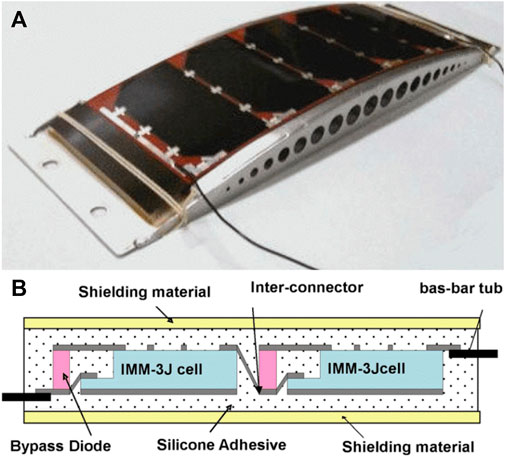
FIGURE 5. A photograph of space module assembly on curved substrate (A) and a cross-sectional view of a module (B). Images adapted from (Yamaguchi et al., 2015).
Moving away from the extra-terrestrial applications, combating climate change and the role of MJSCs in terrestrial applications is of utmost importance. Terrestrial CPV installations utilizing MJSCs delivers the highest power output among all the other solar cell technologies as the irradiance of the sunlight upon a solar cell is directly proportional to the power generation. By concentrating the sunlight onto the MJSC, the sunlight-to-energy conversion efficiency can be effectively increased, and the efficiency-to-cost ratio can be decreased. CPV installations are split into three categories according to their concentration power: high (HCPV), medium (MCPV) and low CPV (LCPV). Commercial HCPV, MCPV, and LCPV has a typical concentration ratio of 100–2000 suns, 10–100 suns, <10 suns respectively (Renno, 2022). CPV installations deliver a high energy yield in geographical locations subject to a high yearly direct normal irradiance (DNI) such as the Middle Eastern countries (Steiner et al., 2022). As with every solar application, initially, Si based solar cells were used instead of MJSCs. In 1981, The Saudi Solar Village photovoltaic power system (PVPS) became the was the first large CPV in operation capable of supplying more than 350 kW of power. This installation used an array point focusing optical system to concentrate sunlight onto the Si solar cells (Salim and Eugenio, 1990). Along with PVPS, ENTECH linear arched optical concentration system also utilized Si solar cells for power generation. These two projects were the pioneering CPV installations that operated successfully for many years during the initial phases of CPV development. Both these systems required Al finned extrusions for the thermal management system as cell cooling is a necessity since Si solar cells degrade rapidly at high temperatures. Even with the cell cooling systems, the Si based solar cells eventually delaminated and failed (Fraas, 2010). PVPS and ENTECH highlighted the short comings as Si based solar cells is limited to only LCPV to MCPV range. In order to harvest more power from the Sun while maintaining competitive efficiency-to-cost ratio of the system, a different approach was required. In 2006, MJSCs passed the fabled 40% efficiency threshold at the time which signaled that after decades of development of MJSCs, their performance can offset the costs required in HCPV systems. This milestone was monumental for MJSCs gaining ground on conventional Si based solar cells for terrestrial applications (Kinsey, 2010).
The most common way to concentrate the light onto solar cells is by using a Fresnel lens (Bett et al., 2006). They were also used in the pioneering PVPS and ENTECH systems for optical concentration. Significant efforts have been conducted to improve the CPV system as a whole along with the MJSCs. Optical systems using Fresnel lenses are constantly being optimized to reduce optical losses, material costs and thermal degradation thus prolonging the life cycle of the system. Optical losses due to UV-induced degradation can also affect the module efficiency (Fernández-Solas et al., 2021). Modern commercial HCPV systems use silicone glass Fresnel lenses than the early acrylic based lenses due to lower costs combined with superior abrasion and UV degradation resistance (Peharz and Bett, 2010). Alternatively, parabolic mirrors (e.g., Cassegrain-type) are also used to concentrate sunlight onto the 3-J solar cells (Figure 6) (Bett et al., 2006).

FIGURE 6. Example of concentrated photovoltaic modules with parabolic mirror optics (Martínez et al., 2017).
In order to consistently focus a high concentration of sunlight onto the MJSCs, a Sun tracker is a necessity. Single-axis trackers or fixed mounts (no-tracking) is a cost-effective solution. However, they limit maximizing the performance of the CPV system because the peak power output gradually decreases when the surface of the panel is not subject to direct incident sunlight. This means that as the position of the Sun changes during the day, the hours of direct normal incident sunlight utilized is lowered causing large power generation fluctuations. Two-axis trackers enable the MJSCs to directly face the Sun throughout the day and thus over the course of the year provide the consistency in power output and capacity factor (Kinsey, 2010). As a result, the investment into two-axis trackers is justified by the performance increase of the CPV system. The optical concentration system consisting of the two-axis tracker and Fresnel lens minimizes the optical losses and efficiently concentrate the sunlight onto the MJSC.
FLATCON CPVs is an example of a modern CPV system (Figure 7A), Fresnel lenses are mounted on to MJSCs to focus sunlight up to 500 suns on each 3-J solar cell with a total area of 3.1 mm2 (Figure 7B). Each solar cell works with a current of 200 mA, producing 0.4 W of power with 0.9 W of heat generated (Dimroth, 2006). Pyron CPV module (Figure 7C) is another example that has the same working principle. In this system, Fresnel lenses and MJSC rows are situated in a flat arrangement to reduce wind load effects during two-axis tracking by rotating the ring structure in the azimuth (Bett et al., 2006). Commercial CPV modules have an efficiency >30% with a lifetime of at least 25 years. Aging of MJSCs in CPV applications is mainly due to moisture and degradation of cell bonding due to high temperatures. Therefore, a cooling system is required to effectively dissipate the generated heat flux otherwise the solar cells or the assembly can be damaged. Cooling or thermal management systems are designed to equip either active cooling using cooling fluids in a heat exchanger or passive cooling via air convection. From a designer’s perspective, passive cooling is more desirable due to less complexity required in designing such a system. However, passive cooling requires relatively large areas to dissipate heat. In a Fresnel optical system, the MJSC is located beneath the lens so an area equivalent to the lens’ aperture is available for efficient heat dissipation. On the other hand, this area is not available for a parabolic concentration system because the MJSCs are located in front of the optics causing additional shading losses (Peharz and Bett, 2010).
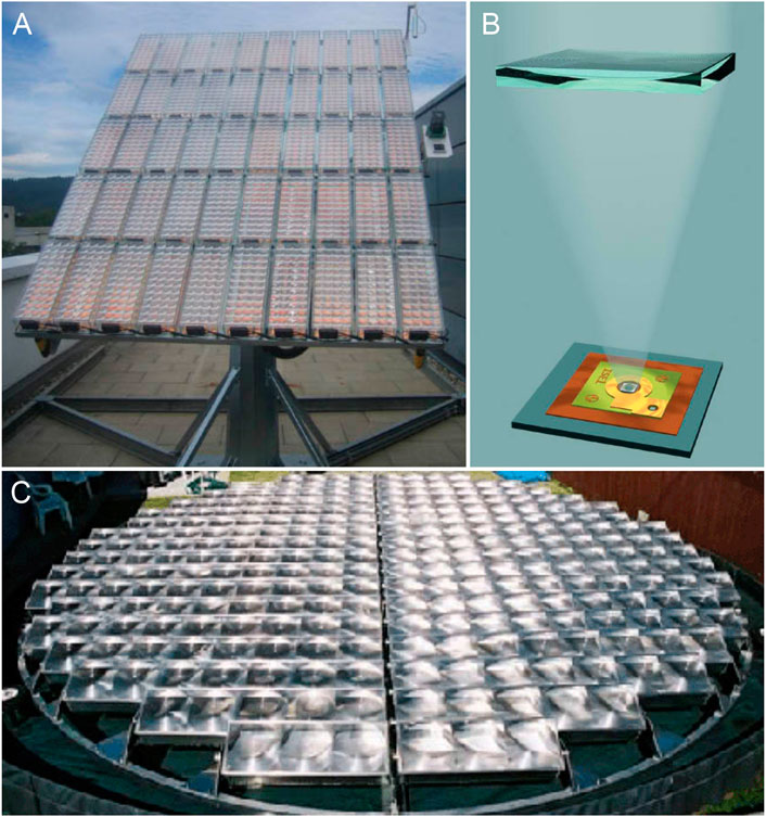
FIGURE 7. Photographs of FLATCON concentrated photovoltaic module (A) and schematics of single solar cell and a lens (B). (C) Photographs of Pyron concentrated photovoltaic module. Images are adapted from (Philipps and Bett, 2014) and (www.pyronsolar.com).
In the future, the goal is to integrate 3-J solar cells for terrestrial applications which includes residential and commercial rooftops and large-scale utility plants (McConnell and Symko-Davies, 2006). However, these envisioned goals come with the inherent challenges faced by 3-J solar cells which have currently forced them into the aforementioned niche applications even though they offer the best performance among all the photovoltaic technologies.
Challenges
Two main challenges are detected for MJSCs. On one side, the high cost of MJSC modules is the main obstacle for overtaking the market dominance of mature Si single junction solar cells, thus restraining MJSCs to niche applications where the surface area is the limiting factor (i.e., space application or unmanned aircrafts and drones). On the other side, increase of MJSC efficiency may outweigh the high cost of MJSCs for long-term solutions in renewable energy sources. So, a trade-off between efficiency and cost needs to be considered for the choice of solar cells.
Increasing efficiency
Commercialized MJSC efficiencies are approximately 30% which is below the S-Q limit for a single junction solar cell. The ideal theoretical efficiency of a 3-J solar cell is approximately 50% under one Sun concentration and approximately 64% for a concentration of 1,000 suns (Figure 8). To increase the efficiencies, more junctions can be deposited with around 75% efficiency for 6 junction solar cells. The efficiencies are limited by concentration, spectrum, and temperature. For example, maximum concentration of 46,000 suns results in theoretical efficiencies only 10–20% higher than under the 1 Sun irradiation. Spectrum tuning has a smaller effect (1–4%) compared to the absolute. Furthermore, ideal efficiencies consider a unity diode factor, infinite shunt resistance, zero series resistance, 100% photon absorption and no recombination, while in reality these factors are far from ideal due to material chemistry and imperfections (Kurtz et al., 2008).
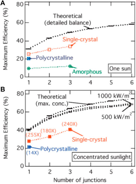
FIGURE 8. Theoretical and champion efficiencies of multijunction solar cells under (A) one sun and (B) concentrated sunlight (Kurtz et al., 2008).
Efficiency is dependent on the quality and durability of materials. Research is being conducted towards material compositions to boost efficiencies with concepts such as Auger generation, hot carriers, and intermediate bandgap materials for high efficiency solar cells. Auger generation materials is a concept which involves the utilization of higher energy photons which are more than twice the bandgap to generate two or more electron-hole pairs. If the excess energy of the primary electron or hole is not dissipated as phonons, this energy can be used to generate another electron-hole pair via impact ionization (Kolodinski et al., 1993). Si-Ge alloy has been identified as a possible Auger generation material (Goetzberger, Luther and Willeke, 2002). Hot carrier solar cells use energy-selective contacts combined with slow carrier cooling absorber to selectively extract carriers before they relax with the lattice vibration thus preventing thermalization losses. Intermediate bandgap solar cells employ the two-step absorption process in addition to the direct band-to-band transition. This is realized by the engineering of an additional band in the middle of the bandgap. Therefore, electrons with lower energy can absorb another photon in the intermediate bandgap and reach the conduction band, thus increasing the overall efficiency of the solar cells (Almosni et al., 2018).
MJSC efficiency is also boosted by minimizing possible losses that can occur in a photovoltaic system. Bulk recombination losses originate from impurities, dislocations, and other defects in the semiconductor absorber, which act as hotspots for non-radiative recombination. The bulk recombination losses can be minimized by ensuring the growth of high-quality epitaxial layers to reduce the density of defects in each MJSC layer (García-Tabarés and Rey-Stolle, 2014). Furthermore, interfacial recombination loss due to lattice mismatching defects is also minimized by optimizing lattice matching growth, inverted epitaxial growth, modifications to BSF or insertion of double heterostructure junctions. Surface passivation layers and double heterostructure junctions are important research topics as they also help minimize surface recombination losses (Yamaguchi, 2015). Alternatively, photon recycling through light trapping can be utilized by deposition of backside mirrors. As a result, optical losses are minimized by doubling the effective distance travelled by the light to get reabsorbed in the semiconductors thus boosting external quantum efficiency of the solar cell (Walker et al., 2015). Finally, in all modern solar cells, ARC is used on the front surface to alter the refractive index and increase the absorption efficiency so novel coatings are constantly under development. Nanostructured alumina (Reuna et al., 2022), SiO2/tantalum pentoxide (Sertel et al., 2019) and zinc oxide (Aé et al., 2010) are some of the ARCs that have been studied for MJSC applications.
Reduction of fabrication costs
In theory, efficiency can be increased by depositing more semiconductor junctions. Recent technoeconomic analysis for III-V//Si MJSCs shows the relationship between efficiency and cost. A 30% efficient two-junction (2-J) GaInP//Si and GaAs//Si solar cell led to a fabrication cost of $4.85/W and $7.17/W respectively. Meanwhile, a 3-J GaInP/GaAs//Si solar cell with 35% efficiency was already up to $8.24/W (Essig et al., 2017). Furthermore, adding four, five or six junctions increases the complexity of fabrication processes to achieve lattice matched epitaxial layers with low defects. Consequently, the fabrication costs can increase exponentially. Given that the fabrication costs of MJSCs are one order of magnitude greater than conventional Si solar cells ($0.3-$0.35/W), the question arises whether more-efficient MJSCs can be chosen for commercial and residential applications.
For example, if 1000 W/m2 is assumed as the solar irradiation per unit area, one 3-J GaInP/GaAs//Si can generate a peak power of 350 W/m2. Assuming an average efficiency of 20% for a conventional Si solar cell, 200 W/m2 of power can be produced. For comparison to generate 1400 W/m2 of power, four 3-J GaInP/GaAs//Si or seven conventional Si solar cells are required. However, the total fabrications costs of 3-J GaInP/GaAs//Si (Essig et al., 2017) still greatly prioritizes the Si solar cell. As a result, MJSCs are only used for military (unmanned aerial vehicles) and aerospace applications (satellites) where there is area and weight constraints rather than costs. In 2018, 3-J solar cells were produced in low volumes in the range of 100s of kW/year to couple MW/year. They accounted for only 0.02% of the market share (Philipps, Warmuth and Al., 2022). Therefore, in order for MJSCs to provide competitive performance-to-cost ratio, it is an absolute necessity of optimization or search for alternate materials and fabrication processes to compete with conventional Si based technologies.
Figure 9 shows that the total manufacturing costs are $100/W for 50 kW/year production and $70/W for 200 kW/year production. The cost difference is due to the building and fixed equipment costs being underutilized for lower installed capacities. The high price per Gram of metal-trimethyl precursors, Ge and As are responsible for the high material costs. Furthermore, lithography has low throughput and high costs per tool which is set around $1–2.5 million. The high costs of MOVPE fabrication prevents the large area deposition required for kW to GW installations to capture a higher percentage of market share. Transfer printing technology provide an extremely low-cost alternative to grow high quality epitaxial layers if they are scaled up (Lumb et al., 2015). Furthermore, lower cost fabrication techniques such as electroplating are active research areas and can reduce the costs associated with contacts (Philipps, Warmuth and Al., 2022).
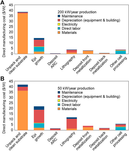
FIGURE 9. Manufacturing costs of III-V//Ge 3-J solar cells for overall production volumes of 200 kW/year (A) and 50 kW/year (B). Images adapted from (Horowitz et al., 2018).
Figure 10 shows the effect of ±20% variation of materials and processes from market values. The largest effect on total costs is the Ge substrate and manufacturing yield. If Au is not recycled, sensitivity to prices increases significantly. Recycling of Ag causes the sensitivity to price fluctuations to decrease significantly showing the importance of recycling processes in the manufacturing costs of 3-J solar cells. The efficiency of the solar cells also influences manufacturing costs as increasing the efficiency from 33% to 34% decreases costs by $2.07/W and decreasing to 32% increases the costs by $2.2/W (Horowitz et al., 2018).
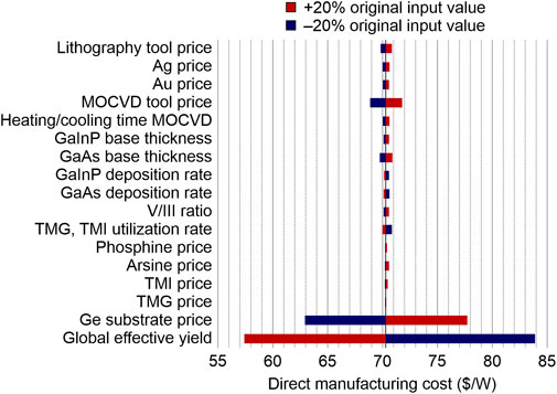
FIGURE 10. Sensitivity of III-V//Ge 3-J solar cells manufacturing costs. Image adapted from (Horowitz et al., 2018).
Ge is the most expensive part of 3-J solar cells at $1,200/kg. Ge extraction is a complex procedure because it is naturally formed as a by-product of sphalerite ores. The multistep procedure includes roasting, leaching and Waelz process to remove zinc impurities followed by chlorination and eventually reduction to Ge (Naumov, 2007). Performance losses in the Ge cell also contributes to the delay of market growth of MJSCs. Therefore, research is being directed to replace Ge cell in the MJSCs. Dilute nitride antimonide sub cells employing InGaP heterolayer have a better lattice and bandgap matching than Ge (Sabnis, Yuen and Wiemer, 2012). Growth of III-V materials on a Si substrate (or wafer bonding) is considered as an alternative because the Si has a larger indirect bandgap of 1.12 eV compared to 0.67 eV of Ge. This enables the excess current to be substantially reduced. Furthermore, the overall current of the 3-J solar cells would not decrease, and Si replacement could lead to higher voltages (Philipps and Bett, 2014). Lastly, another incentive for the replacement of Ge to Si in the modern 3-J solar cells is that Si is lighter, stronger, abundant while having a lower cost compared to Ge (Derendorf et al., 2013).
Cost reduction via recycling
Availability of scarce raw materials such as Ga or In and high price of Ge are limiting the performance-to-cost ratio of MJSCs in the market. In and Ga are constituents of III-V absorbers. In is also used in TCO electrodes. Thick Ge film represents the bottom cell in commercial MJSCs. The good news is that these materials are recoverable and hence giving them a second life while reducing the costs of the next set of 3-J solar cells.
The recycling process begins with the disassembly of the CPV module as shown in Figure 11. The module housing and support structure can be reused in new modules if it is not damaged. Since Fresnel lenses are constructed from poly (methyl methacrylate) (PMMA), they can be recovered by crushing then pyrolysis at temperatures higher than 160°C. MMA of purity >98% can be obtained when PMMA is depolymerized with molten lead at a temperature of 500°C.
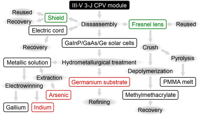
FIGURE 11. Simplified recycling process for III-V//Ge 3-J solar cells. Marked in red are the most critical components to recycle due to price or toxicity. Marked in green are the components, which can be reused if not mechanically damaged. Image adapted from (Wang, 2016).
Hydrometallurgical treatment is used to separate each MJSC layer by etching with nitric acid. Although hydrometallurgical treatment is commercially viable with low emissions, it is the most expensive and time-consuming process due to the multiple absorption and separation steps. Each chemical process steps must also be adapted to respective technology (Chowdhury et al., 2020). So, research is being conducted towards vacuum blasting, tenside chemistry, leaching, flotation, etching for material separation as they provide an alternative with tradeoffs to mitigate environmental concerns by reducing chemical usage with low-energy consumption and processing times (Chowdhury et al., 2020).
Rare elements of Ga and In compounds are separated by extraction, ion-exchange or precipitation with an electrowinning process used to refine Ga and In to high purity of 99.99%. Since electrolysis is energy and time-consuming process, alternative solutions include wet refining and two-step vacuum distillation method (Xu et al., 2021). Ga can be purified to 99.9999% with float zoning or Czochralski process which is also used to grow single crystal Si (Moskalyk, 2003).
Arsenic (As) is a biohazard so treatment with As containing solution is necessary for recycling with minimum risk. As solution reacts with sulfur dioxide and arsenic trioxide is extracted from the reduced solution (Wang, 2016). Due to these complex, time consuming and potentially dangerous processes, the cost of recycling is also higher than competing solar cell technologies. This makes the cost-to-efficiency ratio of MJSCs at least for terrestrial applications less desirable so it is necessary for research to be directed in the development of alternative recycling methods to drive down the costs.
Future
Perovskite solar cells
Recently, perovskite group of semiconductors has emerged as new group of materials for photovoltaic applications. Drastic development from a power conversion efficiency of 3.8% recorded in 2009 (Kojima et al., 2009) for the first perovskite solar cell to a record of 25.7% in 2022 (Min et al., 2021) has enabled their potential use in MJSCs.
Perovskites have an ABX3 chemical structure where A and B are cations and X is a halide. The flexibility in the choice of cations and anions in the perovskite structure and the use of cheaper raw materials cause the costs to be relatively low compared to III-V semiconductors thus enabling a lower cost-to-efficiency ratio (Snaith, 2013), which is the single most important parameter in delaying the widespread commercialization of III-V MJSCs. Methylammonium (MA) and formamidinium (FA) are usually the A cation, with Pb or tin (Sn) as the B cation. The X halide is varied between bromine (Br), chlorine (Cl) and iodine (I). Methylammonium lead iodide (MAPbI3) has been identified as a cost-effective, high-performance semiconductor absorber and has undergone major research over the last decade. MAPbCl3, MAPbBr3, MASnI3, FAPbI3 and FASnI3 round up the other popular organic-inorganic lead or tin halide perovskites (Ansari, Qurashi and Nazeeruddin, 2018). These perovskites exhibit high absorption coefficients which are comparable to GaAs semiconductors (De Wolf et al., 2014), high electron-hole diffusion lengths which can even exceed 1 μm (Stranks et al., 2013), high charge-carrier mobilities and low exciton binding energy (Ansari, Qurashi and Nazeeruddin, 2018). Compared to Si, MAPbI3 have one and two magnitudes higher absorption coefficient in the green and red region respectively. Only in the blue region, Si and MAPbI3 perovskites have equivalent absorption coefficients (Yakunin et al., 2017). Next, the bandgap of the perovskite can easily be tuned by changing the halide composition. For example, by changing the I-to-Br ratio in the perovskite MAPb(Br3–xIx), the band gap can be adjusted from 1.6 to 2.3 eV. Like III-V materials, this is a major advantage, perovskites display over Si (Yakunin et al., 2017). The scale up from lab to industrial scale for large commercial deployment of perovskite based MJSCs is realistically attainable in the near future as this is a hot spot for research and development as a spill-over effect from the success of perovskite based single junction solar cells (Li and Zhang, 2020). In addition, the fabrication of perovskite films via solution process has fewer steps, is inexpensive and the film composition can easily be adjusted. This is another major advantage over Si and III-V semiconductors (Niu, Guo and Wang, 2015). As a result, perovskites can be a viable alternative to replace III-V semiconductors partly or fully in a MJSC at least for commercial and residential applications.
However, like any technology, perovskites have their own drawbacks, which need to be ameliorated before wide-scale deployment. The most pending problem of perovskites is their environmental instability. Especially, perovskites are extremely sensitive to oxygen and moisture, with are inevitable contaminants during the assembling and testing procedures. For example, MAPbI3 hydrolyzes instantly causing irreversible degradation in the presence of trace amounts of moisture. Hence, almost all the manufacturing is conducted in small quantities inside a glovebox filled with an inert gas such as argon, increasing the fabrication and labor costs (Niu, Guo and Wang, 2015; Wang et al., 2016). Temperature instability of perovskites is incompatible with stable solar cell operation. For examples, perovskite layers delaminate already at temperatures as low as 85°C in ambient atmosphere (Conings et al., 2015; Wang et al., 2016). In other study, fast degradation of MAPbI3 is observed as the temperature gets near 100°C, but it is even more alarming that MAPbI3 slowly decomposes to PbI2 at elevated temperatures even under an inert atmosphere such as argon (Philippe et al., 2015). Finally, as perovskites are derived from dye-sensitized solar cell architectures, they also have the same ultraviolet (UV) light degradation. The charge collection efficiency of TiO2 electron transport layer deteriorated over a period of 5 h when tested in an ambient condition of 1 Sun illumination and AM 1.5G spectrum. This deterioration is due the electrons injected into the TiO2 being trapped in deep lying unoccupied states (Leijtens et al., 2013; Wang et al., 2016).
The aforementioned stability problems highlights that for space and CPV applications, perovskites are unable to match the superior thermal and chemical stability offered by III-V semiconductors because under UV light, high temperatures and extreme pressure conditions, perovskites can decompose due to changes in the crystalline phases causing the absorbers to be unstable (Niu, Guo and Wang, 2015).
At the current level of development, the extremely short lifetime resulting from the ambient stability issues seems worlds apart compared to the high end-of-life efficiencies offered by Si and III-V based solar cells even after 25–30 years. Researchers are continuously working on developing novel solutions for the aforementioned problems in perovskites for the commercialization and the possibility of dethroning Si as the leader in solar cell technologies. After all, no one could have predicted such a monumental rise of perovskites in such a short period of time.
Combining photovoltaic technologies
III-V, perovskites and Si are co-dependent on each other for the pathway to success of the MJSCs in the terrestrial market. It is well-established that Ge in the bottom sub cell of a traditional 3-J solar cell adds up to a hefty chunk of the total cost. Si was the first candidate to be studied as a possible replacement for Ge in a III-V MJSC, promising up to a 70% of the cell cost reduction (D’Souza et al., 2011). On one hand, Si bottom cell is more beneficial towards high efficiency MJSCs because of the voltage and fill factor gain by the substitution. This is a consequence of a better bandgap and current matching provided by the Si (Derendorf et al., 2013). On the other hand, formation of defects during compound growth along with problems related to reliability and reproducibility has hindered Si into competing with other tandem cell technologies rather than being the outright best candidate as in single-junction solar cells. However, processes such as heteroepitaxial growth, mechanical stacking and wafer bonding ensures that III-V//Si produces the best performance at competitive costs (Yu, Rabelo and Yi, 2022). In 2021, the 35.9% efficiency was achieved for 3-J III-V absorbers with Si when measured under terrestrial AM 1.5G spectrum. This monumental record is a proof that there is a real possibility in the near future that the MJSCs will be competing with conventional single-junction solar cells in terms of production costs due to higher material availability (Schygulla et al., 2022).
Perovskite materials can also be combined with III-V or Si in a tandem solar cell and the performance can be boosted to >25% by collecting the reflected light (i.e., bifacial configuration) as well as structuring of solar cell layers (De Bastiani et al., 2021). All-perovskite MJSCs have been realized based on three perovskite cells with different bandgaps (Figure 12A) (Xiao et al., 2020). This prototype MJSC already shows efficiencies of >20%, despite imperfections within the layers (e.g., polycrystallinity) and at the lattice-mismatched interfaces (Figure 12B). It is predicted that 3-J perovskite solar cells can reach efficiencies of 33% (Hörantner et al., 2017). However, as mentioned in the previous section, the inherent stability problems of perovskites need to be immediately addressed to scale up from lab scale to industry.
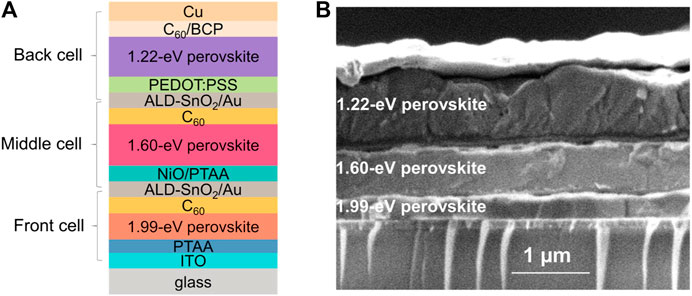
FIGURE 12. (A) Schematics and (B) cross-sectional scanning electron micrograph of 3-J solar cell with perovskite materials for all absorber layers (Xiao et al., 2020).
Among other emerging photovoltaic technologies are chalcogenide quantum dots (Lin et al., 2019) and organic solar cells (Mazzio and Luscombe, 2015). Lead (II) sulfide (PbS) quantum dots (QDs) are the most studied, bringing unique advantage of size-dependent electronic properties, such as the band gap (Gocalińska et al., 2010) and mobility (Yazdani et al., 2014). Both QDs and organic materials possess additional fabrication advantage of liquid-phase deposition of thin films via, spin-coating, spray-drying or printing (Lin et al., 2021). Due to easy non-vacuum fabrication, QDs and organic solar cell layers can be integrated with other photovoltaic technologies, for example amorphous Si cell reaching efficiencies of >12% for PbS/Si (Kashyap et al., 2020) and 11.7% for organic/Si (Roland et al., 2015) tandem cells.
Optimizing production lines
Increasing production volume can cause an overall cost reduction due to learning-by-doing and economies-of-scale. MOVPE tool costs are predicted to reduce by 10–15% with high production volumes and increased automation. Furthermore, improved tool utilization can lower total labor costs (Figure 13). For example, when increasing the growth rate from 15 μm/h to 60 μm/h with a 95% yield for MOVPE and HVPE, the production costs reduce by $0.5/W for 2-J solar cells. Research and development of a continuous, in-line gallium nitride (GaN) MOVPE reactor which increased the batch sizes for LED growth resulted in a higher throughput thus reducing the costs by half (Figure 13, third bar) (Horowitz et al., 2018). This technique doesn’t exist in 2022 for MJSC growth but is feasible in the future. Dynamic-HVPE has demonstrated growth rates of 195 μm/h, where the reaction chambers are spatially separated enabling the production of high-quality materials with high throughput. The pseudo-in-line reactor has been demonstrated for 2-J solar cells in lab scale which could be scaled to use each chamber for deposition of preceding layers (Horowitz et al., 2018).
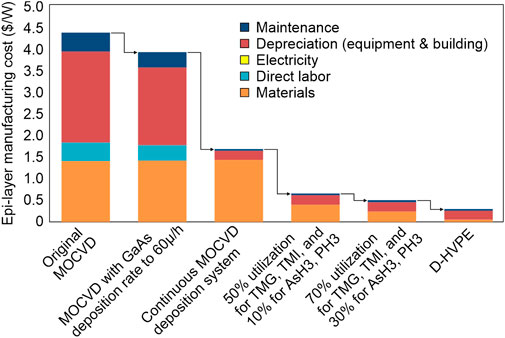
FIGURE 13. Effects of fabrication optimization (increased material utilization and throughput) on the cost of III-V//Ge multijunction solar cells. Image adapted from (Horowitz et al., 2018).
Future of concentrated photovoltaics
Along with wind and hydropower, MJSCs in CPV installations can contribute to the renewable energy harvesting using solar power to accelerate the energy transition for a sustainable future. The current CPV market is valued at $740 million and is expected to double in 2026. MJSCs for CPV have a lower upfront cost than wind farms and hydropower dams. Among other advantages are the potential double use of land for CPV such as agriculture or more stable energy production during the day owing to solar position tracking. In contrast, hydropower and wind require the displacement of land and habitats during construction and operation causing high negative environmental impact.
On the other hand, disadvantages include CPVs requiring additional energy storage for discharge during off-peak hours, whereas dams can use pumped storage. Next, CPV installations have lower efficiencies compared to wind (45%) and hydropower (90%). Additional optical losses and lack of technology standardization increases the risk as MJSCs are new technologies with a small history of production in industrial scale. Lastly, CPV can only be installed with high DNI so there is a limited choice of locations for CPV modules (Wiesenfarth et al., 2017).
Conclusion
Single junction solar cells are limited by the S-Q limit at a maximum efficiency of approximately 33%. MJSCs are proven to be the champion among all the solar cell technologies both in laboratory and module scale with the use of multiple semiconductor absorbers to attain record efficiencies. MJSCs have a record efficiency of 47.1% compared to Si (26.7%). MJSCs offer double the performance with research and development directed into novel concepts and materials to further increase the efficiency by reducing thermalization and transmission losses. These records are currently set by altering doping, elementary compositions, and thickness in high quality epitaxially grown III-V semiconductors. However, complexity of fabrication, rarity of crucial materials and the low throughput resulting from slow growth rates has deterred the wide-spread commercialization of MJSCs for CPV applications due to the high manufacturing costs.
Preceding sections in this review arrives at one major conclusion. Manufacturing costs of the MJSCs needs to decrease by an order of magnitude to overtake other photovoltaic technologies. Innovation in fabrication processes, research into alternative materials such as Si and perovskites and recycling techniques is undoubtedly the key to propel MJSCs to gain ground on conventional Si and thin film technologies in the next decade. As a result, leading the acceleration of energy transition to meet climate and energy demand goals from the solar energy front. Since perovskite solar cells have not yet been commercialized on a wide-scale, fully III-V based, or III-V//Si MJSCs are recommended for the immediate integration in power grids as these are mature technologies that has a proven track record of performance. The exponential development of perovskites over the past decade is expected to continue and, in the future, they can provide a cost-effective alternative to III-V materials either in a fully perovskite, III-V//perovskite or a perovskite//Si tandem MJSC.
On the other hand, currently, MJSCs hold several niche applications for which long-term stability, resistance to radiation damage and limited surface area are more important factors than the module price. In addition, each MJSC module is profitable, e.g., taking a lifetime of 25 years, the return cost is predicted as double the initial manufacturing costs (Hussain and Kim, 2019). Finally, energy payback time for MJSCs is on par with the mainstream Si solar cells, between 8 and 16 months depending on the operational site and configuration (Peharz and Dimroth, 2005). Thus, demonstrating that fabrication costs are the only impeding factor for MJSCs to grasp more of the terrestrial applications for solar energy.
Author contributions
Conceptualization: MY; writing—original draft: AB; writing—review and editing: MY and AB.
Funding
This work was supported by the ETH Innovedum Grant. Open access funding provided by ETH Zurich.
Acknowledgments
We would like to acknowledge Sarah E. Shephard, Karin Brown, Pia Scherrer, and Lenny Winkel for their support in developing a course “Chemistry of Devices and Technologies” for which this review article has been originally prepared.
Conflict of interest
The authors declare that the research was conducted in the absence of any commercial or financial relationships that could be construed as a potential conflict of interest.
Publisher’s note
All claims expressed in this article are solely those of the authors and do not necessarily represent those of their affiliated organizations, or those of the publisher, the editors and the reviewers. Any product that may be evaluated in this article, or claim that may be made by its manufacturer, is not guaranteed or endorsed by the publisher.
References
Adams, W. G., and Day, R. E. (1877). V. The action of light on selenium. Proc. R. Soc. Lond. 25 (171–178), 113–117.
Aé, L., Kieven, D., Chen, J., Klenk, R., Rissom, T., Tang, Y., et al. (2010). ZnO nanorod arrays as an antireflective coating for Cu(In, Ga)Se2 thin film solar cells. Prog. Photovolt. Res. Appl. 18 (3), 209–213. doi:10.1002/pip.946
Almosni, S., Delamarre, A., Jehl, Z., Suchet, D., Cojocaru, L., Giteau, M., et al. (2018). Material challenges for solar cells in the twenty-first century: Directions in emerging technologies. Sci. Technol. Adv. Mater. 19 (1), 336–369. doi:10.1080/14686996.2018.1433439
Ansari, M. I. H., Qurashi, A., and Nazeeruddin, M. K. (2018). Frontiers, opportunities, and challenges in perovskite solar cells: A critical review. J. Photochem. Photobiol. C Photochem. Rev. 35, 1–24. doi:10.1016/j.jphotochemrev.2017.11.002
Bailey, S., and Raffaelle, R. (2010). “Chapter 18. Space solar cells and applications,” in Solar Cells their Applicatipons. Editors L. Fraas, and L. Partain. 2nd ed., 397–424.
Becquerel, M. E. (1839). Mémoire sur les effets électriques produits sous l’influence des rayons solaires. Comptes rendus Hebd. séances l’Académie Sci. 9, 561–567.
Bett, A. W., Burger, B., Dimroth, F., Siefer, G., and Lerchenmuller, H. (2006). “High-concentration PV using III-V solar cells,” in 2006 IEEE 4th World Conference on Photovoltaic Energy Conference, 615–620. doi:10.1109/WCPEC.2006.279530
Bett, A. W., Dimroth, F., Guter, W., Hoheisel, R., Oliva, E., Philipps, S. P., et al. (2009). Highest efficiency multi-junction solar cell for terrestrial and space applications. space 25 (258), 30–36.
Bett, A. W., Philipps, S. P., Essig, S., Heckelmann, S., Kellenbenz, R., Klinger, V., et al. (2013). “Overview about technology perspectives for high efficiency solar cells for space and terrestrial applications,” in 28th European photovoltaic solar energy conference and exhibition, 1–6.
Bin Rafiq, M. K. S., Amin, N., Alharbi, H. F., Luqman, M., Ayob, A., Alharthi, Y. S., et al. (2020). WS2: A new window layer material for solar cell application. Sci. Rep. 10 (1), 771. doi:10.1038/s41598-020-57596-5
Boucher, J. W., Greenaway, A. L., Ritenour, A. J., Davis, A. L., Bachman, B. F., Aloni, S., et al. (2015). “Low-cost growth of III–V layers on si using close-spaced vapor transport,” in 2015 IEEE 42nd Photovoltaic Specialist Conference (PVSC), 1–4. doi:10.1109/PVSC.2015.7356079
Chapin, D. M., Fuller, C. S., and Pearson, G. L. (1954). A new silicon p‐n junction photocell for converting solar radiation into electrical power. J. Appl. Phys. 25 (5), 676–677. doi:10.1063/1.1721711
Chiu, P. T., Law, D. C., Woo, R. L., Singer, S. B., Bhusari, D., Hong, W. D, et al. (2014). “35.8% space and 38.8% terrestrial 5J direct bonded cells,” in 2014 IEEE 40th Photovoltaic Specialist Conference (PVSC), 11–13. doi:10.1109/PVSC.2014.6924957
Chowdhury, M. S., Rahman, K. S., Chowdhury, T., Nuthammachot, N., Techato, K., Akhtaruzzaman, M., et al. (2020). An overview of solar photovoltaic panels’ end-of-life material recycling. Energy Strategy Rev. 27, 100431. doi:10.1016/j.esr.2019.100431
Colter, P., Hagar, B., and Bedair, S. (2018). Tunnel junctions for III-V multijunction solar cells review. Crystals 8, 445. doi:10.3390/cryst8120445
Conings, B., Drijkoningen, J., Gauquelin, N., Babayigit, A., D'Haen, J., D'Olieslaeger, L., et al. (2015). Intrinsic thermal instability of methylammonium lead trihalide perovskite. Adv. Energy Mat. 5 (15), 1500477. doi:10.1002/aenm.201500477
Cotal, H., Fetzer, C., Boisvert, J., Kinsey, G., King, R., Hebert, P., et al. (2009). III–V multijunction solar cells for concentrating photovoltaics. Energy Environ. Sci. 2 (2), 174–192. doi:10.1039/B809257E
Cozzi, L., Erdogan, M., and Goodson, T. (2021). Global energy review 2021. Available at: https://www.iea.org/reports/global-energy-review-2021.
De Bastiani, M., Mirabelli, A. J., Hou, Y., Gota, F., Aydin, E., Allen, T. G., et al. (2021). Efficient bifacial monolithic perovskite/silicon tandem solar cells via bandgap engineering. Nat. Energy 6 (2), 167–175. doi:10.1038/s41560-020-00756-8
De Wolf, S., Holovsky, J., Moon, S. J., Loper, P., Niesen, B., Ledinsky, M., et al. (2014). Organometallic halide perovskites: Sharp optical absorption edge and its relation to photovoltaic performance. J. Phys. Chem. Lett. 5 (6), 1035–1039. doi:10.1021/jz500279b
Derendorf, K., Essig, S., Oliva, E., Klinger, V., Roesener, T., Philipps, S. P., et al. (2013). Fabrication of GaInP/GaAs//Si solar cells by surface activated direct wafer bonding. IEEE J. Photovolt. 3 (4), 1423–1428. doi:10.1109/JPHOTOV.2013.2273097
Dimroth, F. (2006). High-efficiency solar cells from III-V compound semiconductors. Phys. Status Solidi 3 (3), 373–379. doi:10.1002/pssc.200564172
D’Souza, S., Haysom, J., Anis, H., and Hinzer, K. (2011). “The down-to-earth future of Si substrate multi-junction concentrator photovoltaics,” in 2011 IEEE Electrical Power and Energy Conference, 57–61. doi:10.1109/EPEC.2011.6070253
Essig, S., Allebe, C., Remo, T., Geisz, J. F., Steiner, M. A., Horowitz, K., et al. (2017). Raising the one-sun conversion efficiency of III–V/Si solar cells to 32.8% for two junctions and 35.9% for three junctions. Nat. Energy 2 (9), 17144. doi:10.1038/nenergy.2017.144
Fernández-Solas, Á., Micheli, L., Almonacid, F., and Fernandez, E. F. (2021). Optical degradation impact on the spectral performance of photovoltaic technology. Renew. Sustain. Energy Rev. 141, 110782. doi:10.1016/j.rser.2021.110782
Fraas, L. (2010). “Chapter 12. Low-concentration crystalline silicon systems,” in Solar Cells their Applications. Editors L. Fraas, and L. Partain. 2nd ed., 273–292.
García-Tabarés, E., and Rey-Stolle, I. (2014). Impact of metal-organic vapor phase epitaxy environment on silicon bulk lifetime for III–V-on-Si multijunction solar cells. Sol. Energy Mater. Sol. Cells 124, 17–23. doi:10.1016/j.solmat.2014.01.034
Geisz, J. F., France, R. M., Schulte, K. L., Steiner, M. A., Norman, A. G., Guthrey, H. L., et al. (2020). Six-junction III–V solar cells with 47.1% conversion efficiency under 143 Suns concentration. Nat. Energy 5 (4), 326–335. doi:10.1038/s41560-020-0598-5
Geisz, J. F., Kurtz, S., Wanlass, M. W., Ward, J. S., Duda, A., Friedman, D. J., et al. (2007). High-efficiency GaInP∕GaAs∕InGaAs triple-junction solar cells grown inverted with a metamorphic bottom junction. Appl. Phys. Lett. 91 (2), 023502. doi:10.1063/1.2753729
Gocalińska, A., Saba, M., Quochi, F., Marceddu, M., Szendrei, K., Gao, J., et al. (2010). Size-dependent electron transfer from colloidal PbS nanocrystals to fullerene. J. Phys. Chem. Lett. 1 (7), 1149–1154. doi:10.1021/jz100116t
Goetzberger, A., Luther, J., and Willeke, G. (2002). Solar cells: Past, present, future. Sol. Energy Mater. Sol. Cells 74 (1), 1–11. doi:10.1016/S0927-0248(02)00042-9
Grovenor, C. R. M. (1998). Microelectronic Materials (1st ed). New York: Routledge. doi:10.1201/9780203747230
Hörantner, M. T., Leijtens, T., Ziffer, M. E., Eperon, G. E., Christoforo, M. G., McGehee, M. D., et al. (2017). The potential of multijunction perovskite solar cells. ACS Energy Lett. 2 (10), 2506–2513. doi:10.1021/acsenergylett.7b00647
Horowitz, K. A., Remo, T. W., Smith, B., and Ptak, A. J. (2018). A techno-economic analysis and cost reduction roadmap for III-V solar cells. doi:10.2172/1484349
Hussain, M. I., and Kim, J.-T. (2019). Energy and economic potential of a concentrated photovoltaic/thermal (CPV/T) system for buildings in South Korea. J. Asian Archit. Build. Eng. 18 (2), 139–144. doi:10.1080/13467581.2019.1606718
Iles, P. A. (2001). Evolution of space solar cells. Sol. Energy Mat. Sol. Cells 68 (1), 1–13. doi:10.1016/S0927-0248(00)00341-X
Irvine, S. (2017). in Solar cells and photovoltaics BT - springer handbook of electronic and photonic materials. Editors S. Kasap, and P. Capper (Cham: Springer International Publishing), 1. doi:10.1007/978-3-319-48933-9_43
Jackson, E. D. (1955). “Areas for improvement of the semiconductor solar energy converter,” in Trans. Intern. Conf. on the Use of Solar Energy-The Scientific Basis, 122.
Jakkala, P., and Kordesch, M. E. (2017). Bandgap tuning and spectroscopy analysis of InxGa(1−x)N thin films grown by RF sputtering method. Mat. Res. Express 4 (1), 016406. doi:10.1088/2053-1591/aa5111
Jingfeng, B., Senlin, L., Guanzhou, L., Meijia, Y., Mingyang, L., Weiping, X., et al. (2015). The epitaxial growth of high efficiency inverted metamorphic triple junction solar cell for CPV application. AIP Conf. Proc. 1679 (1), 40002. doi:10.1063/1.4931513
Kao, Y.-C., Chou, H. M., Hsu, S. C., Lin, A., Lin, C. C., Shih, Z. H., et al. (2019). Performance comparison of III–V//Si and III–V//InGaAs multi-junction solar cells fabricated by the combination of mechanical stacking and wire bonding. Sci. Rep. 9 (1), 4308. doi:10.1038/s41598-019-40727-y
Karam, N. H., Fetzer, C. M., Liu, X-Q., Steiner, M. A., and Schulte, K. L. (2019). ‘Metamorphic growth and multijunction III-V solar cells’, metalorganic vapor phase epitaxy (MOVPE). Wiley Online Books, 149–173. doi:10.1002/9781119313021.ch5
Kashyap, S., Pandey, R., Madan, J., and Sharma, R. (2020). Design and simulation of a-Si:H/PbS colloidal quantum dots monolithic tandem solar cell for 12% efficiency. Phys. Status Solidi A 217 (20), 2000252. doi:10.1002/pssa.202000252
Kinsey, G. (2010). High-concentration, III–V multijunction solar cells, solar Cells and their applications, 293–312.
Kojima, A., Teshima, K., Shirai, Y., and Miyasaka, T. (2009). Organometal halide perovskites as visible-light sensitizers for photovoltaic cells. J. Am. Chem. Soc. 131 (17), 6050–6051. doi:10.1021/ja809598r
Kolodinski, S., Werner, J. H., Wittchen, T., and Queisser, H. J. (1993). Quantum efficiencies exceeding unity due to impact ionization in silicon solar cells. Appl. Phys. Lett. 63 (17), 2405–2407. doi:10.1063/1.110489
Kurtz, S., Myers, D., McMahon, W. E., Geisz, J., and Steiner, M. (2008). A comparison of theoretical efficiencies of multi-junction concentrator solar cells. Prog. Photovolt. Res. Appl. 16 (6), 537–546. doi:10.1002/pip.830
Leijtens, T., Eperon, G. E., Pathak, S., Abate, A., Lee, M. M., and Snaith, H. J. (2013). Overcoming ultraviolet light instability of sensitized TiO2 with meso-superstructured organometal tri-halide perovskite solar cells. Nat. Commun. 4 (1), 2885. doi:10.1038/ncomms3885
Li, H., and Zhang, W. (2020). Perovskite tandem solar cells: From fundamentals to commercial deployment. Chem. Rev. 120 (18), 9835–9950. doi:10.1021/acs.chemrev.9b00780
Li, J., Aierken, A., Liu, Y., Zhuang, Y., Yang, X., Mo, J. H., et al. (2021). A brief review of high efficiency III-V solar cells for space application. Front. Phys. 8, 631925 doi:10.3389/fphy.2020.631925
Lin, W. M. M., Yarema, M., Liu, M., Sargent, E., and Wood, V. (2021). Nanocrystal quantum dot devices: How the lead sulfide (PbS) system teaches us the importance of surfaces. CHIMIA 75, 398. doi:10.2533/chimia.2021.398
Lin, W. M. M., Yazdani, N., Yarema, O., Volk, S., Yarema, M., Kirchartz, T., et al. (2019). Simulating nanocrystal-based solar cells: A lead sulfide case study. J. Chem. Phys. 151 (24), 241104. doi:10.1063/1.5129159
Lorenczik, S., Jorquera Copier, J., Hevia-Koch, P., and Hungerford, Z. (2022). Electricity market report. Available at: https://www.iea.org/reports/electricity-market-report-january-2022/.
Lumb, M. P., Meitl, M., Fisher, B., Burroughs, S., Schmieder, K. J., Gonzalez, M., et al. (2015). “Transfer-printing for the next generation of multi-junction solar cells,” in 2015 IEEE 42nd Photovoltaic Specialist Conference (PVSC), 1–6. doi:10.1109/PVSC.2015.7356146
Luque, A., and Hegedus, S. (2011). Handbook of photovoltaic science and engineering. John Wiley & Sons.
Martínez, M., Sánchez, D., Calvo-Parra, G., Gil, E., Hipólito, A., de Gregorio, F., et al. (2017). “8 years of CPV: ISFOC CPV plants, long-term performance analysis and results,“ in AIP Conference Proceedings 1881, 020007. doi:10.1063/1.5001406
Mazzio, K. A., and Luscombe, C. K. (2015). The future of organic photovoltaics. Chem. Soc. Rev. 44 (1), 78–90. doi:10.1039/C4CS00227J
McConnell, R., and Symko-Davies, M. (2006). “Multijunction photovoltaic technologies for high-performance concentrators,” in 2006 IEEE 4th World Conference on Photovoltaic Energy Conference, 733–736. doi:10.1109/WCPEC.2006.279560
Miles, R. W. (2006). Photovoltaic solar cells: Choice of materials and production methods. Vacuum 80 (10), 1090–1097. doi:10.1016/j.vacuum.2006.01.006
Min, H., Lee, D. Y., Kim, J., Kim, G., Lee, K. S., Kim, J., et al. (2021). Perovskite solar cells with atomically coherent interlayers on SnO2 electrodes. Nature 598 (7881), 444–450. doi:10.1038/s41586-021-03964-8
Moskalyk, R. R. (2003). Gallium: The backbone of the electronics industry. Miner. Eng. 16 (10), 921–929. doi:10.1016/j.mineng.2003.08.003
Naumov, A. V. (2007). World market of germanium and its prospects. Russ. J. Non-ferrous Met. 48 (4), 265–272. doi:10.3103/S1067821207040049
Nikoletatos, J., and Halambalakis, G. (2018). in Chapter III-1-B - standards, calibration, and testing of PV modules and solar cells. Editor S. A. P. Kalogirou (Academic Press), 1155–1182. doi:10.1016/B978-0-12-809921-6.00033-1
Niu, G., Guo, X., and Wang, L. (2015). Review of recent progress in chemical stability of perovskite solar cells. J. Mat. Chem. A Mat. 3 (17), 8970–8980. doi:10.1039/C4TA04994B
NOAA National Centers for Environmental Information (2021). State of the climate: Monthly global climate report for july 2021. Available at: https://www.ncei.noaa.gov/access/monitoring/monthly-report/global/202107 (Accessed September 8, 2022).
Oh, G., Kim, Y., Lee, S. J., and Kim, E. K. (2020). Broadband antireflective coatings for high efficiency InGaP/GaAs/InGaAsP/InGaAs multi-junction solar cells. Sol. Energy Mater. Sol. Cells 207, 110359. doi:10.1016/j.solmat.2019.110359
Pakhanov, N. A., Andreev, V. M., Shvarts, M. Z., and Pchelyakov, O. P. (2018). State-of-the-art architectures and technologies of high-efficiency solar cells based on III–V heterostructures for space and terrestrial applications. Optoelectron. Instrum. Proc. 54 (2), 187–202. doi:10.3103/S8756699018020115
Peharz, G., and Bett, A. W. (2010). Solar cells and their applications. High-Concentration Fresnel Lens Assemblies Syst. 217, 313.
Peharz, G., and Dimroth, F. (2005). Energy payback time of the high-concentration PV system FLATCON, Prog. Photovolt. Res. Appl., 13(7), 627–634. doi:10.1002/pip.621
Philippe, B., Park, B. W., Lindblad, R., Oscarsson, J., Ahmadi, S., Johansson, E. M. J., et al. (2015). Chemical and electronic structure characterization of lead halide perovskites and stability behavior under different exposures—a photoelectron spectroscopy investigation. Chem. Mat. 27 (5), 1720–1731. doi:10.1021/acs.chemmater.5b00348
Philipps, S. P., and Bett, A. W. (2014). III-V Multi-junction solar cells and concentrating photovoltaic (CPV) systems, Adv. Opt. Technol., 3(5–6), 469–478. doi:10.1515/aot-2014-0051
Philipps, S. P., Dimroth, F., and Bett, A. W. (2018). in Chapter I-4-B - high-efficiency III–V multijunction solar cells. Editor S. A. B. T.-M. H. Kalogirou (Academic Press), 439–472. doi:10.1016/B978-0-12-809921-6.00012-4
Philipps, S., Warmuth, W., and Al, E. (2022). ISE photovoltaics report. Available at: https://www.ise.fraunhofer.de/en/publications/studies/photovoltaics-report.html.
Rehman, A. ur, Lee, Sang Hee, and Lee, Soo Hong (2016). Silicon space solar cells: Progression and radiation-resistance analysis. J. Korean Phys. Soc. 68 (4), 593–598. doi:10.3938/jkps.68.593
Renno, C. (2022). Characterization of spherical optics performance compared to other types of optical systems in a point-focus CPV system. Therm. Sci. Eng. Prog. 29, 101201. doi:10.1016/j.tsep.2022.101201
Reuna, J., Hietalahti, A., Aho, A., Isoaho, R., Aho, T., Vuorinen, M., et al. (2022). Optical performance assessment of nanostructured alumina multilayer antireflective coatings used in III–V multijunction solar cells. ACS Appl. Energy Mat. 5 (5), 5804–5810. doi:10.1021/acsaem.2c00133
Roland, S., Neubert, S., Albrecht, S., Stannowski, B., Seger, M., Facchetti, A., et al. (2015). Hybrid organic/inorganic thin-film multijunction solar cells exceeding 11% power conversion efficiency. Adv. Mat. 27 (7), 1262–1267. doi:10.1002/adma.201404698
Rühle, S. (2016). Tabulated values of the Shockley–Queisser limit for single junction solar cells. Sol. Energy 130, 139–147. doi:10.1016/j.solener.2016.02.015
Sabnis, V., Yuen, H., and Wiemer, M. (2012). High-efficiency multijunction solar cells employing dilute nitrides. AIP Conf. Proc. 1477 (1), 14–19. doi:10.1063/1.4753823
Salim, A. A., and Eugenio, N. N. (1990). A comprehensive report on the performance of the longest operating 350 kW concentrator photovoltaic power system. Sol. Cells 29 (1), 1–24. doi:10.1016/0379-6787(90)90011-S
Schmieder, K. J., Yakes, M. K., Bailey, C. G., Pulwin, Z., Lumb, M. P., Hirst, L. C., et al. (2014). “Analysis of GaAs solar cells at High MOCVD growth rates,” in 2014 IEEE 40th Photovoltaic Specialist Conference (PVSC), 2130–2133. doi:10.1109/PVSC.2014.6925345
Schygulla, P., Muller, R., Lackner, D., Hohn, O., Hauser, H., Blasi, B., et al. (2022). Two-terminal III–V//Si triple-junction solar cell with power conversion efficiency of 35.9 % at AM1.5g. Prog. Photovoltaics. 30 (8), 869–879. doi:10.1002/pip.3503
Sertel, T., Ozen, Y., Baran, V., and Ozcelik, S. (2019). Effect of single-layer Ta2O5 and double-layer SiO2/Ta2O5 anti-reflective coatings on GaInP/GaAs/Ge triple-junction solar cell performance. J. Alloys Compd. 806, 439–450. doi:10.1016/j.jallcom.2019.07.257
Simon, J., Young, D., and Ptak, A. (2014). “Low-cost III–V solar cells grown by hydride vapor-phase epitaxy,” in 2014 IEEE 40th Photovoltaic Specialist Conference (PVSC), 538–541. doi:10.1109/PVSC.2014.6924977
Snaith, H. J. (2013). Perovskites: The emergence of a new era for low-cost, high-efficiency solar cells. J. Phys. Chem. Lett. 4 (21), 3623–3630. doi:10.1021/jz4020162
Song, J. S., Choi, Y., Seo, S., Oh, D., Cho, M., Yao, T., et al. (2004). Wet chemical cleaning process of GaAs substrate for ready-to-use. J. Cryst. Growth 264 (1), 98–103. doi:10.1016/j.jcrysgro.2003.12.063
Steiner, M., Mathur, P., Sarkar, S., and Siefer, G. (2022). Improving the accuracy of energy yield calculations of tandem solar cell-based CPV-modules. Prog. Photovoltaics. 30 (3), 257–262. doi:10.1002/pip.3480
Stranks, S. D., Eperon, G. E., Grancini, G., Menelaou, C., Alcocer, M. J. P., Leijtens, T., et al. (2013). Electron-hole diffusion lengths exceeding 1 micrometer in an organometal trihalide perovskite absorber. Science 342 (6156), 341–344. doi:10.1126/science.1243982
Sugiura, H., Amano, C., Yamamoto, A., and Yamaguchi, M. (1988). Double heterostructure GaAs tunnel junction for a AlGaAs/GaAs tandem solar cell. Jpn. J. Appl. Phys. (2008). 27 (2R), 269–272. doi:10.1143/jjap.27.269
Sun, Y., Faucher, J., Jung, D., Vaisman, M., McPheeters, C., Sharps, P., et al. (2016). “Thermal stability of GaAs solar cells for high temperature applications,” in 2016 IEEE 43rd Photovoltaic Specialists Conference (PVSC), 2385–2388. doi:10.1109/PVSC.2016.7750068
Sun, Z., Chen, X., He, Y., Li, J., Wang, J., Yan, H., et al. (2022). Toward efficiency limits of crystalline silicon solar cells: Recent progress in high-efficiency silicon heterojunction solar cells. Adv. Energy Mater. 12 (23), 2200015. doi:10.1002/aenm.202200015
Tanabe, K. (2009). A review of ultrahigh efficiency III-V semiconductor compound solar cells: Multijunction tandem, lower dimensional, photonic up/down conversion and plasmonic nanometallic structures. Energies 2, 504–530. doi:10.3390/en20300504
Walker, A. W., Hohn, O., Micha, D. N., Wagner, L., Helmers, H., Bett, A. W., et al. (2015). Impact of photon recycling and luminescence coupling on III–V single and dual junction photovoltaic devices. J. Photonics Energy 5 (1), 053087. doi:10.1117/1.JPE.5.053087
Wang, D., Wright, M., Elumalai, N. K., and Uddin, A. (2016). Stability of perovskite solar cells. Sol. Energy Mater. Sol. Cells 147, 255–275. doi:10.1016/j.solmat.2015.12.025
Wang, T.-Y. (2016). in Recycling of solar cell materials at the end of life BT - advances in solar photovoltaic power plants. Editors M. R. Islam, F. Rahman, and W. Xu (Berlin, Heidelberg: Springer Berlin Heidelberg), 287–317. doi:10.1007/978-3-662-50521-2_11
Wiesenfarth, M., Philipps, S. P., Bett, A. W., Horowitz, K., and Kurtz, S. (2017). Current status of concentrator photovoltaic (CPV) technology. Available at: https://www.ise.fraunhofer.de/en/publications/studies/studie-current-status-of-concentrator-photovoltaic-cpv-technology.html.
Wolf, M. (1960). Limitations and possibilities for improvement of photovoltaic solar energy converters: Part I: Considerations for earth’s surface operation. Proc. IRE 48 (7), 1246–1263. doi:10.1109/jrproc.1960.287647
Xiao, K., Wen, J., Han, Q., Lin, R., Gao, Y., Gu, S., et al. (2020). Solution-processed monolithic all-perovskite triple-junction solar cells with efficiency exceeding 20%. ACS Energy Lett. 5 (9), 2819–2826. doi:10.1021/acsenergylett.0c01184
Xu, S., Wang, G., Fan, J., Wang, Z., Zhang, J., Chen, J., et al. (2021). Preparation of high purity indium by chemical purification: Focus on removal of Cd, Pb, Sn and removal mechanism. Hydrometallurgy 200, 105551. doi:10.1016/j.hydromet.2020.105551
Yakunin, S., Shynkarenko, Y., Dirin, D. N., Cherniukh, I., and Kovalenko, M. V. (2017). Non-dissipative internal optical filtering with solution-grown perovskite single crystals for full-colour imaging. NPG Asia Mat. 9 (9), e431. doi:10.1038/am.2017.163
Yamaguchi, H., Ijichi, R., Suzuki, Y., Ooka, S., Shimada, K., Takahashi, N., et al. (2015). “Development of space solar sheet with inverted triple-junction cells,” in 2015 IEEE 42nd Photovoltaic Specialist Conference (PVSC), 1–5. doi:10.1109/PVSC.2015.7356138
Yamaguchi, M. (2015). Fundamentals and R&D status of III-V compound solar cells and materials. Phys. Status Solidi C 12 (6), 489–499. doi:10.1002/pssc.201400216
Yamaguchi, M., Takamoto, T., and Araki, K. (2008). “Present and future of super high efficiency multi-junction solar cells,” in Proc.SPIE. doi:10.1117/12.784117
Yazdani, N., Bozyigit, D., Yarema, O., Yarema, M., and Wood, V. (2014). Hole mobility in nanocrystal solids as a function of constituent nanocrystal size. J. Phys. Chem. Lett. 5 (20), 3522–3527. doi:10.1021/jz5015086
Yoshikawa, K., Kawasaki, H., Yoshida, W., Irie, T., Konishi, K., Nakano, K., et al. (2017). Silicon heterojunction solar cell with interdigitated back contacts for a photoconversion efficiency over 26%. Nat. Energy 2 (5), 17032. doi:10.1038/nenergy.2017.32
Yu, S., Rabelo, M., and Yi, J. (2022). A brief review on III-V/Si tandem solar cells. Trans. Electr. Electron. Mat. 23 (4), 327–336. doi:10.1007/s42341-022-00398-5
Keywords: III-V semiconductors, 3-J solar cells, concentrated photovoltaics, cost reduction, recycling, efficiency, fabrication
Citation: Baiju A and Yarema M (2022) Status and challenges of multi-junction solar cell technology. Front. Energy Res. 10:971918. doi: 10.3389/fenrg.2022.971918
Received: 17 June 2022; Accepted: 23 August 2022;
Published: 29 September 2022.
Edited by:
Salah Kamel, Aswan University, EgyptReviewed by:
Edmund Udemba, Gelişim Üniversitesi, TurkeyRafiqul Islam, Bangladesh Agricultural University, Bangladesh
Copyright © 2022 Baiju and Yarema. This is an open-access article distributed under the terms of the Creative Commons Attribution License (CC BY). The use, distribution or reproduction in other forums is permitted, provided the original author(s) and the copyright owner(s) are credited and that the original publication in this journal is cited, in accordance with accepted academic practice. No use, distribution or reproduction is permitted which does not comply with these terms.
*Correspondence: Maksym Yarema, eWFyZW1hbUBldGh6LmNo