 Gopinathan Vishnupriya
 Pichandi Sathya
- School of Electronics Engineering, Vellore Institute of Technology, Vellore, Tamil Nadu, India
This research explores an innovative dual-absorber solar cell design that incorporates MAGeI3 and CsSnI3 layers, aiming to achieve efficiency levels that exceed those of current single-junction solar cells. Simulations conducted with SCAPS-1D software identified optimal layer thicknesses for both materials, resulting in a maximum efficiency that significantly surpasses previously documented values for similar configurations. When considering defect densities, the optimized parameters revealed a strong open-circuit voltage, a high short-circuit current density, and an impressive fill factor, leading to a noteworthy overall efficiency even at certain defect levels. The enhanced performance of this dual-absorber design is attributed to the complementary bandgaps of the materials, which improve light absorption and charge carrier dynamics. Specifically, the smaller bandgap of CsSnI3 allows for more effective harvesting of lower-energy photons, and the higher bandgap of MAGeI3 helps in the absorption of higher-energy photons, while the dual-layer structure minimizes recombination losses. Further analyses of quantum efficiency and current-voltage characteristics support the architecture’s potential to approach theoretical efficiency limits. This study suggests that the proposed dual-absorber configuration holds considerable promise for advancing solar cell technology and warrants further experimental validation.
1 Introduction
In recent years, thin-film solar cells have garnered substantial research interest due to improvements in efficiency and cost-effective manufacturing methods, making them ideal for diverse applications such as thermal energy and photovoltaic systems (Omid and Cora, 2020; Salve, 2020; Maoucha et al., 2023). Their advantages over traditional wafer-based technologies include reduced material consumption and lower production costs. Growing efforts are directed at discovering novel materials to improve the efficiency-to-cost ratio. Lead-based perovskites, in particular, have exhibited exceptional optical and electrical properties, including a high absorption coefficient, low exciton binding energy, tunable bandgap, long diffusion lengths, and high carrier mobility, all achievable through low-cost fabrication (Roy et al., 2022; Teixeira et al., 2022). Thin-film solar cells can be manufactured via high-throughput and energy-efficient deposition techniques such as sputtering and chemical vapor deposition, which are better suited to scale than those used in silicon wafer technologies. Valeti et al. (2024) emphasized optimizing these processes for cost-effectiveness. Lead-based perovskite solar cells have reached conversion efficiencies of up to 26.7% (NREL, 2025; Interactive Best Research-Cell Efficiency Chart Photovoltaic Research, 2025), but they face major challenges like degradation and toxicity. Kamat et al. (2017) highlighted the urgency of solving stability and toxicity issues to make lead-free alternatives viable.
To overcome these limitations, researchers are turning to lead-free perovskites such as cesium germanium halides, which offer advantages like bandgap tunability, strong optical absorption, and improved conductivity (Dureja et al., 2022). Dureja et al. (2022) used SCAPS-1D simulations to design a Cs2SnI6-based solar cell, achieving 19.9% efficiency. Similarly, materials like MAGeI3 (CH3NH3GeI3) and CsSnGeI3 are gaining traction due to their high absorption in the visible–infrared range and greater stability than MAPbI3 (Nalianya et al., 2021; Jan and Noman, 2023; Moone and Sharifi, 2024). Hybrid germanium-based perovskites show comparable photovoltaic performance to lead- and tin-based counterparts (Kumari et al., 2024) and have been studied with various electron transport layers (ETLs) and hole transport layers (HTLs) for optimal PCE (Panjikaran et al., 2024). To further boost efficiency, dual-absorber structures were introduced, stacking materials with different bandgaps to absorb a broader solar spectrum and reduce energy losses (Hemalatha et al., 2023). Bhattarai et al. (2023) simulated an MASnI3/CsSnGeI3 dual-absorber design, achieving 31.53% efficiency by optimizing absorber thicknesses. Maoucha et al. (2023) combined MASnI3 and CsSnGeI3 with TiO2 and Spiro-OMeTAD as transport layers to achieve 24.57% efficiency with a JSC of 28.11 mA/cm2, a VOC of 1.32 V, and a fill factor of 90.37%.
AlZoubi et al. (2023) studied MAGeI3 cells with ZnOS and PEDOT-WO3 transport layers, reaching nearly 16% efficiency. Jan and Noman (2023) explored planar and inverted structures of MAGeI3 using SCAPS-1D and concluded that the inverted structure, especially with SnO2 as the ETL and CuAlO2 as the HTL, yielded a PCE of 25.43%, a VOC of 1.77 V, a JSC of 16.18 mA/cm2, and an FF of 89.02%. Focusing on CsSnI3, Ravidas et al. (2023) emphasized its potential due to a 1.3 eV bandgap, strong absorption, and high mobility. Their SCAPS-1D and DFT simulations showed superior performance with HTLs like Spiro-OMeTAD and CuI. Hossain et al. (2023a) and Hossain et al. (2023b) investigated over 70 architectures using CsSnI3 and various ETLs (e.g., IGZO, WS2, TiO2, and C60), identifying ITO/ETL/CsSnI3/CuI/Au as the most promising.
The dual-absorber design marks a pivotal step forward in perovskite solar cell (PSC) development by expanding the absorption range and boosting PCE. Innovations like Ca3NCl3/Ca3SbI3 absorbers further exemplify this progress, achieving improved VOC, JSC, FF, and overall efficiency, which was approximately 30.22%, compared to individual absorber simulation (Ghosh et al., 2024; 2025).
Despite these benefits, insufficient transport layers can result in significant degradation due to energy and lattice mismatches. Consequently, innovative design strategies are crucial to address these issues and improve the performance of lead-free perovskite solar cells. This study introduces an innovative lead-free perovskite solar cell design featuring a dual-absorber architecture composed of methylammonium germanium iodide (MAGeI3) and cesium tin iodide (Cs2SnI3). The cell utilizes MAGeI3 as the wide bandgap front absorber (Eg ≈ 1.9 eV) (Jeon et al., 2021) and Cs2SnI3 as the narrow bandgap rear absorber (Eg ≈ 1.3 eV) (Jeon et al., 2021), allowing for complementary light absorption from the visible to near-infrared spectrum.
The direct stacking of these materials creates a novel heterojunction interface, marking a first in fully lead-free perovskite photovoltaics. This layered architecture is distinct from conventional single-absorber PSCs or tandem cells, as it simplifies fabrication while achieving efficiencies exceeding 36%, surpassing the Shockley–Queisser limit, in this work. Energy band alignment analysis reveals a small conduction band offset (+0.2 eV) and a favorable valence band offset (−0.4 eV), which facilitates efficient charge separation and extraction without requiring a buffer layer. This approach simplifies the device structure while promoting low toxicity and cost-effectiveness. Additionally, simulations provide insights into interfacial properties, carrier dynamics, and optimization parameters, underscoring the potential of this architecture as a sustainable alternative in photovoltaic technology. Figure 1 shows the workflow of the simulated dual absorber architecture using SCAPS-1D and also the working points.
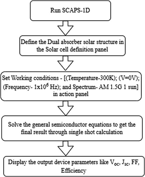
Figure 1. Workflow of dual architecture simulation through SCAPS-1D.
2 Numerical model and design
Despite the promising properties of hybrid lead perovskite solar cells, they face significant challenges, primarily due to their susceptibility to degradation and the inherent toxicity of lead (Osman et al., 2021; Moone and Sharifi, 2024). To address these issues, researchers have shifted their focus toward non-lead perovskite materials, with cesium germanium halide perovskites emerging as promising alternatives. These materials have demonstrated favorable characteristics, including tunable bandgaps, enhanced optical absorption, and brilliant optical conductivity (Maoucha et al., 2023; Panjikaran et al., 2024). In this work, CsSnI3 and MAGeI3 have been utilized as a double absorber layer and explored various parameters that are reported further.
2.1 Materials
The triumphant development of non-lead perovskites such as MAGeI3 (CH3NH3GeI3) and CsSnI3 has paved the way for high-throughput thin-film solar cells (Hemalatha et al., 2023; Panjikaran et al., 2024). These materials exhibit compelling electrical, optical, and processing properties that rival or surpass those of their lead-based counterparts. Specifically, they offer advantages such as bandgap tunability, large carrier mobility, strong visible–infrared range absorption coefficients, and improved stability compared to MAPbI3.
2.2 Simulation
The Solar Cell Capacitance Simulator (SCAPS) is a widely recognized and utilized software environment for solar modeling research, developed by the Electronic and Information Systems Department at Ghent University in Belgium (Burgelman et al., 2025; Al-Hattab et al., 2022). This simulation tool employs fundamental equations, including electron and hole Poisson equations, continuity equations, and transport equations, to model the capture of sunlight and the subsequent generation, movement, and extraction of electron-hole pairs in solar devices.
One of SCAPS’s key strengths is its flexibility, allowing researchers to design and simulate specific solar devices by manipulating a broad range of material properties. The simulation outputs are invaluable for assessing the impact of various factors on device performance and for gaining insights into crucial solar cell characteristics. These include material defect density, defect placement, recombination rates, and band gap alignment across different layers of the device (Burgelman et al., 2004; Burgelman et al., 2025).
The versatility of SCAPS makes it an essential tool in addressing a wide spectrum of fundamental questions in both materials science and device physics related to solar cell technology. By enabling detailed simulations and analyses, SCAPS contributes significantly to the advancement of solar cell research and development.
The behavior and characteristics of charge carriers within solar devices are fundamentally described by three key equations:
a) The Poisson equation
b) The Continuity equation
c) The Transport equation
These three equations collectively form the mathematical foundation for understanding and modeling the movement, distribution, and interactions of electrons and holes in solar cell structures. They provide a comprehensive framework for analyzing the electrostatic potential, charge carrier dynamics, and current flow within photovoltaic devices.
Fundamental equations used in the SCAPS-1D simulation software for modelling solar cell devices include
a) Carrier Continuity Equation: This equation describes the change in hole and electron concentrations over time, considering current densities, recombination, and generation processes (Islam et al., 2021).
In Equations 1, 2, Jp and Jn are hole and electron current densities, respectively.
R(x) and G(x) are recombination and generation processes, respectively.
b) Diffusion–Drift Equations: These equations describe the current densities for holes and electrons in terms of carrier concentrations, mobilities, and diffusion constants.
In the above Equations 3, 4,
c) Poisson Equation: This equation relates the electrostatic potential to charge carrier concentrations and doping densities in the semiconductor.
Poisson equation is given in the Equation 5, where V(x) is the electrostatic potential,
3 Device structure
The solar cell device structure investigated in this study comprises multiple layers, each serving a specific function to optimize the overall performance. Figure 2 shows the model of the proposed structure. The front electrode is composed of aluminum (Al), which provides a robust and conductive surface for electron collection. Beneath the Al layer, fluorine-doped tin oxide (FTO) is employed as the window layer due to its excellent transparency and conductivity, allowing maximum light penetration while facilitating electron transport. The electron transport layer (ETL) is made of zinc oxide (ZnO), which efficiently transports electrons from the perovskite absorber layers to the FTO.
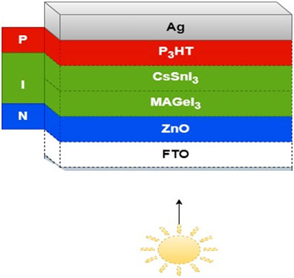
Figure 2. Device structure of the proposed model.
The core of the device consists of two perovskite materials: methylammonium germanium iodide (MAGeI3) and cesium tin iodide (CsSnI3). These materials are strategically combined to enhance light absorption across a broader spectrum, leveraging their complementary bandgaps. This combination not only improves the absorption efficiency but also aids in defect passivation and charge carrier mobility. The hole transport layer (HTL) is composed of poly (3-hexylthiophene) (P3HT), which effectively transports holes to the back electrode. Finally, silver (Ag) is used as the back electrode, providing a high work function contact for efficient hole collection.
The integration of CsSnI3 and MAGeI3 within the device structure is particularly noteworthy. These perovskite materials exhibit high absorption coefficients and good charge carrier mobility, which are crucial for efficient photovoltaic performance. Their bandgap alignment facilitates a graded bandgap structure, driving charge carriers toward their respective electrodes and reducing recombination losses. This innovative combination aims to leverage the strengths of both materials, resulting in a more efficient and stable solar cell.
3.1 Working mechanism
The working mechanism of the proposed device is shown in Figure 3. When photons with energy greater than or equal to the band gap of the absorber layers (MAGeI3 and CsSnI3) fall on the solar cell, they excite electrons from the valence band to the conduction band, creating electron–hole pairs. In the MAGeI3 layer, photons with energy greater than 1.78 eV excite electrons from the valence band (−5.7 eV) to the conduction band (−3.92 eV). These excited electrons then move through the MAGeI3 layer to the ZnO layer. Similarly, in the CsSnI3 layer, photons with energy greater than 1.4 eV excite electrons from the valence band (−5.0 eV) to the conduction band (−3.6 eV). The electrons in the conduction band of CsSnI3 move toward the ZnO layer, while the holes left in the valence band of CsSnI3 move toward the P3HT layer.
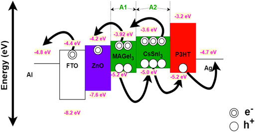
Figure 3. Band diagram of the proposed model showing the working mechanism.
The electrons that reach the ZnO layer are collected by the FTO layer and then move toward the Al electrode, while the holes that reach the P3HT layer are collected by the Ag electrode. This movement of electrons and holes ensures efficient charge separation and collection, converting light into electrical energy. The energy band diagram helps visualize this process by showing the energy levels and the direction of electron and hole movement, with curved arrows indicating the pathways for electrons and holes. This mechanism utilizes the different band gaps of the absorber layers to capture a broader spectrum of sunlight, enhancing the efficiency of the solar cell.
4 Results and discussion
The input property values of the proposed model are given below in Table 1. These are the optimized values received for the maximum efficiency generating device with and without consideration of the defect densities.
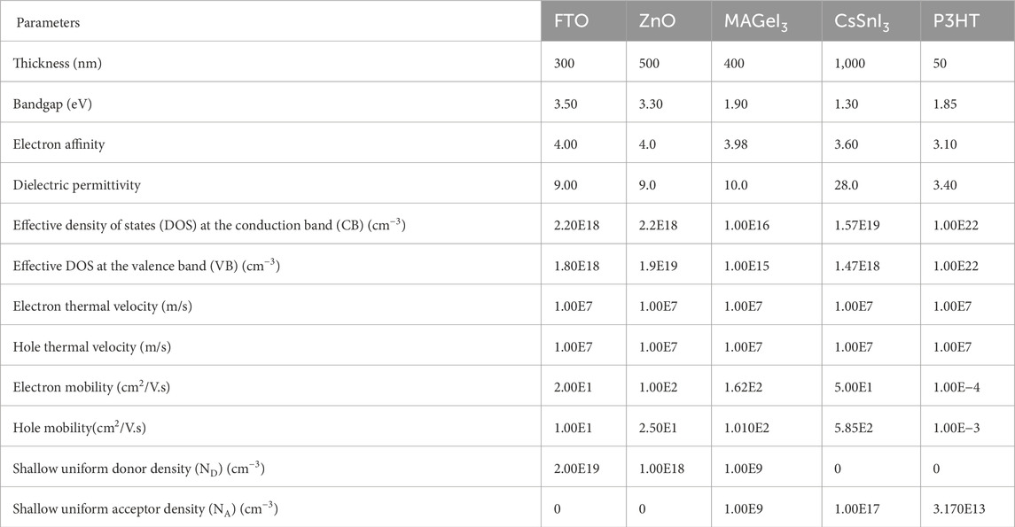
Table 1. Parameters of the proposed model measured under one sun illumination.
4.1 Effect of CsSnI3 and MAGeI3 thickness changes
The thicknesses of the absorber layers of CsSnI3 and MAGeI3 were varied and plotted, and the effects of changing the thicknesses were investigated. The opto-electronic characteristics were studied under the AM1.5 illumination. The plots presented in Figures 4A–D illustrate the behavioral patterns of open-circuit voltage (VOC), short-circuit current density (JSC), fill factor, and efficiency as the thickness of the CsSnI3 layer is varied from 200 nm to 1,000 nm. It is observed that with an increase in the thickness of the CsSnI3 layer, both VOC and fill factor exhibit a slight decreasing trend, while the current and efficiency curves show an upward trend. This might be because of the band alignment mismatch, due to which interfacial recombination can occur. The optimal results are achieved with a CsSnI3 thickness of 1,000 nm, yielding values of VOC = 1.23 V, JSC = 34.79 A, a fill factor of 84.35%, and an efficiency of 36.37%, which represent the highest values recorded to date. On the other hand, no significant changes were seen when we varied the thickness of the MAGeI3 layer.
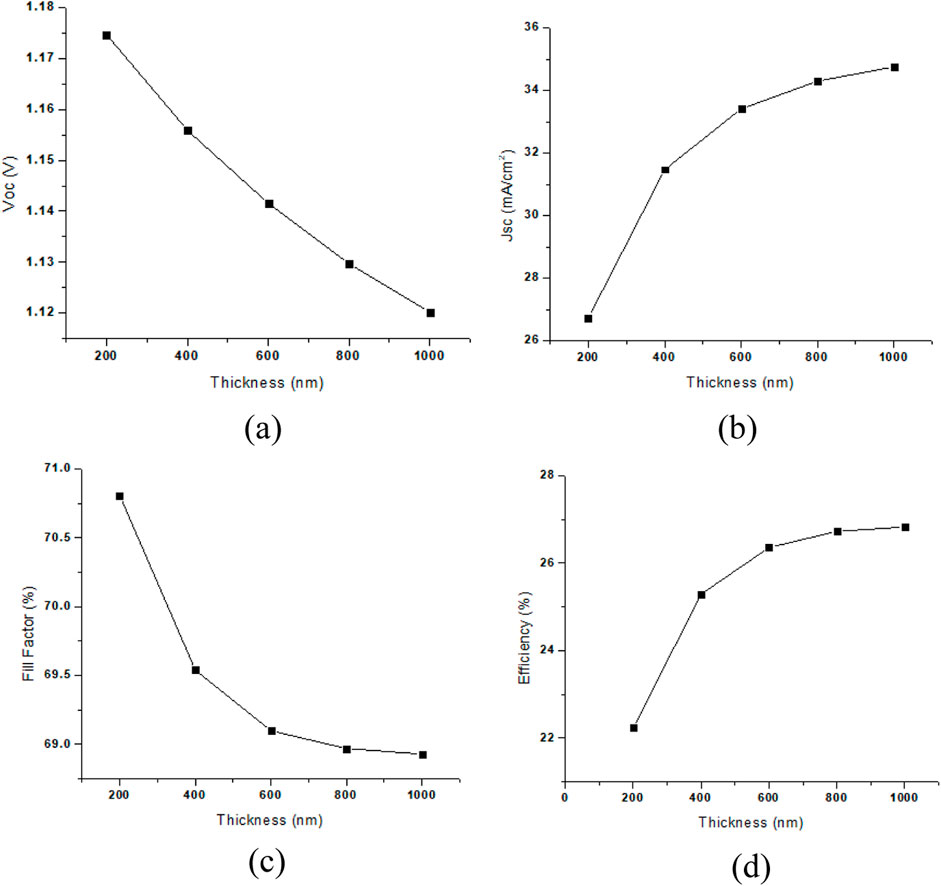
Figure 4. (A) Change in VOC with respect to the variation in CsSnI3 thickness; (B) change in JSC with respect to the variation in CsSnI3 thickness; (C) change in fill factor with respect to the change in CsSnI3 thickness; (D) change in efficiency with respect to the thickness change in CsSnI3.
4.2 Effects of variation in P3HT thickness
In this proposed model, the hole transport layer P3HT thickness is varied from 0.01 µm to 0.1 µm, and the results are given in Table 2. It is observed that the optimum performance of the device is achieved at the P3HT layer thickness of 0.01 µm. In the experimental aspect, acquiring a thickness of 10 nm is impractical, so the HTL thickness is fixed at 50 nm.
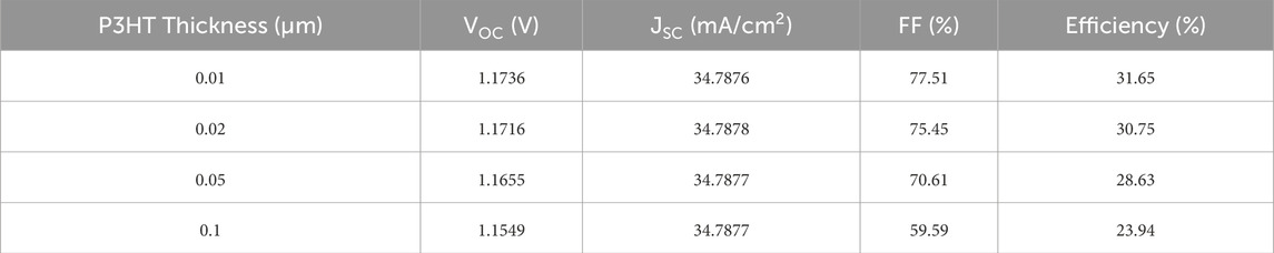
Table 2. Variation of P3HT thickness.
4.3 Effects of defect density in the CsSnI3 and MAGeI3 layers
Figure 5 shows the difference in the device performance with and without the defects. We investigated the incorporation of defect levels in CsSnI3 and MAGeI3 layers, ranging from 1 × 10¹⁰ to 1 × 10¹⁴, and analyzed their impact on open-circuit voltage (VOC), short-circuit current density (JSC), fill factor, and overall device efficiency. The resulting graphs are shown in Figures 6A–D. The observed trend indicates that both VOC and JSC remain relatively stable up to a defect concentration of 1 × 10¹², after which a decline is noted. Conversely, the fill factor exhibits a decreasing trend with increasing defect levels up to 1 × 10¹², followed by a slight improvement. When we also consider the MAGeI3 layer, the device efficiency also decreases, as anticipated in the presence of defects. Consequently, we determine the optimal defect level to be 1 × 10¹².
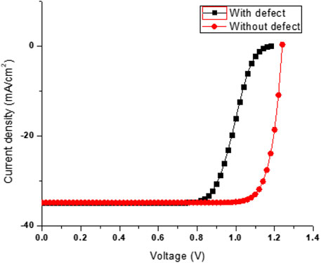
Figure 5. Device performance with and without defects.
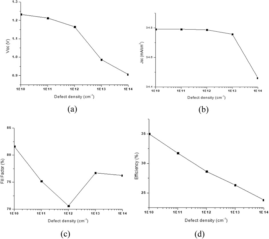
Figure 6. (A) Effect of defect density variation on VOC; (B) effect of defect density variation on JSC; (C) effect of defect density variation on fill factor; (D) effect of defect density variation on device efficiency.
4.4 Effects of temperature variation on the proposed device
The density of states in the conduction and valence bands varies with temperature, as follows in the Equations 6–8, where T0 represents the default temperature, set at 300 K, where the parameter value should be defined in SCAPS-1D. Similarly, the thermal velocity (Vth) is also influenced by temperature, as shown in the following equations. All other parameters are considered to be independent of temperature. The diffusion coefficient used in the calculations, given by
Figure 7 shows J–V (current density vs. voltage) curves for different temperatures, each represented by a distinct color and symbol. As temperature increases, we observe a slight shift in the curves, indicating changes in the device’s electrical characteristics. The open-circuit voltage (VOC) appears to decrease slightly with increasing temperature, which is typical for solar cells due to increased carrier recombination at higher temperatures. However, the short-circuit current density (Jsc) seems to increase with temperature, likely due to enhanced carrier generation. The overall shape of the curves suggests that the fill factor may also be affected by temperature changes, potentially improving slightly at higher temperatures. These temperature-dependent variations in VOC, JSC, and fill factor collectively influence the device’s efficiency, with the optimal operating temperature likely falling within the measured range. Table 3 shows the values of the parameters.
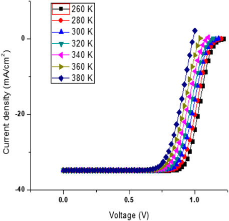
Figure 7. Device performance with increasing temperature from 260 K to 380 K.
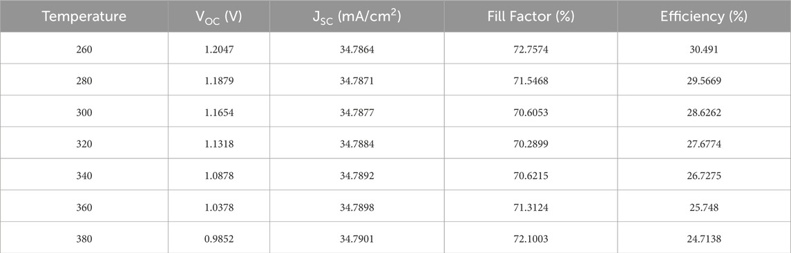
Table 3. Solar parameters with respect to temperature variation.
We also investigated the effects of temperature variation on the device, systematically varying the temperature from 260 K to 380 K. Figure 7 illustrates the impact of temperature changes on open-circuit voltage (VOC), short-circuit current density (JSC), fill factor, and device efficiency. It is observed that VOC exhibits a slight decrease, while JSC increases with rising temperature. This behavior can be attributed to changes in carrier mobility as the temperature increases. The fill factor decreases until approximately 320 K, after which it begins to rise. In contrast, device efficiency decreases linearly with increasing temperature. This pattern is evident in Figures 8A–D.
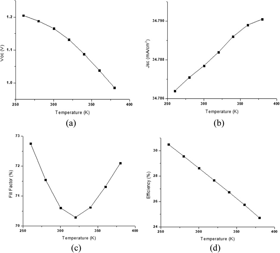
Figure 8. (A) Effect of temperature variation in VOC; (B) effect of temperature variation on JSC; (C) effect of temperature variation on fill factor; (D) effect of temperature variation on device efficiency.
4.5 Effect of dopant concentration
In the proposed device, when the dopant concentration of the CsSnI3 absorber layer was varied from
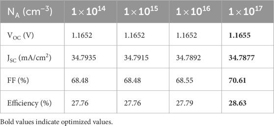
Table 4. Device parameters with varied dopant concentrations.
4.6 Effects of parasitic resistances
Series and shunt resistances are critical parameters in solar cells affecting their efficiency. The former is due to the current movement through the cell’s emitter and base as well as contact resistances. High series resistance reduces the fill factor and JSC, impacting the overall performance of the device.
On the other hand, shunt resistance arises due to manufacturing defects. If the shunt resistance is low, it can create alternate current paths, reducing voltage and current flow, particularly under low light conditions, resulting in significant power losses. Ideally, it is desired that the series resistance should be minimum, and the shunt resistance should be maximum.
4.6.1 Effect of series resistance
In this proposed model, the series resistance was varied from 0 Ω to 10 Ω, respectively, by fixing RSH at 1030 Ω-cm2. Table 5 gives the respective values of solar parameters. The pattern observed is that an increase in series resistance affects JSC and fill factor, thus affecting the overall efficiency.
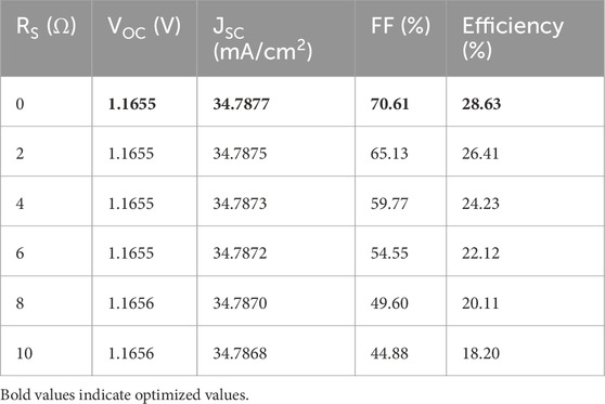
Table 5. Device performance while varying RS, when RSH is fixed at 1030 Ω-cm2.
4.6.2 Effect of shunt resistance
In this proposed model, shunt resistance (RSH)is varied from 10 Ω-cm2 to 1010 Ω-cm2, respectively, by fixing series resistance (RS) at 0.5 Ω. Table 6 gives the values of solar parameters with respect to shunt resistance change. The pattern observed is that, as shunt resistance increases, each parameter improves, and thus the overall performance of the device also improves. Table 6 shows the pattern.
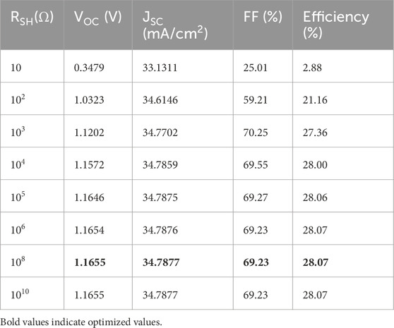
Table 6. Device performance while varying RSH, when RS is fixed at 0.5 Ω
4.7 Effect of quantum efficiency
Quantum efficiency in solar cells measures how efficiently incident photons are converted into electric current. It is typically expressed as a combination of external quantum efficiency (EQE) and internal quantum efficiency (IQE). The former is attributed to optical losses, and the latter reflects the efficiency of charge carrier collection from absorbed photons. Different absorber layers significantly impact quantum efficiency (QE). The choice of materials affects absorption characteristics and recombination rates, influencing overall efficiency.
Replacing a single layer of MAGeI3 with double layers of MAGeI3 and CsSnI3 can enhance the quantum efficiency of solar devices. This configuration benefits from the complementary bandgaps, improving light absorption and charge carrier dynamics.
CsSnI3, with its smaller bandgap, allows for better harvesting of lower-energy photons, potentially increasing overall efficiency beyond that of MAGeI3 alone. The combination can also reduce recombination losses, further boosting performance. Figure 9 shows the comparison of the two devices, one with a single junction of MAGeI3 and one device with dual-absorber layers of MAGeI3 and CsSnI3. The latter shows a better result, promising good practical output.
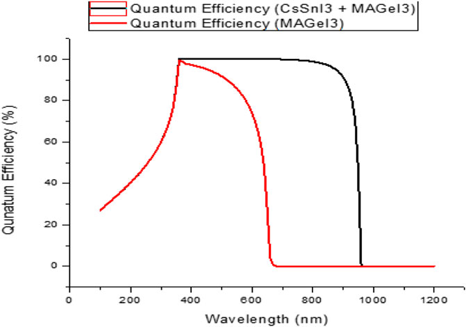
Figure 9. Comparison of quantum efficiency of the device with a single junction of MAGeI3 with the QE of a device with a double layer junction (MAGeI3+CsSnI3).
5 Conclusion
In this study, two absorber layers, specifically MAGeI3 and CsSnI3, were utilized as a dual-absorber configuration. Simulations conducted using SCAPS-1D software indicated that the optimal thickness for MAGeI3 is 0.4 µm, while for CsSnI3, it is 1.0 µm, achieving a maximum efficiency of 36.37% under defect-free conditions, the highest reported to date. Further investigations incorporating defect densities in each layer and also interfacial defect densities revealed optimal solar parameters of Voc = 1.1475 V, Jsc = 34.79 mA/cm2, FF = 69.61%, and efficiency = 27.78% at a defect density of
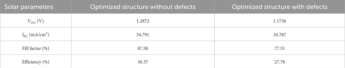
Table 7. Optimized structure parameters before and after adding defect density
Discussion is warranted in bringing this configuration to the experimental set-up because this architecture is to be constructed through sequential deposition, which can pose stability issues and interfacial defects. This can be another bottleneck to be overcome and is a problem worthy of further attention.
Data availability statement
The datasets presented in this study can be found in online repositories. The names of the repository/repositories and accession number(s) can be found in the Supplementary Material.
Author contributions
VG: formal analysis, investigation, methodology, software, writing – original draft, and writing – review and editing. SP: conceptualization, formal analysis, methodology, software, supervision, writing – original draft, and writing – review and editing.
Funding
The author(s) declare that no financial support was received for the research and/or publication of this article.
Acknowledgments
I would like to express my sincere gratitude to my guide, Sathya ma’am, for her invaluable guidance, encouragement, and continuous support throughout the course of this research. I also extend my heartfelt thanks to Vellore Institute of Technology, Vellore, for providing the resources and a conducive environment that made this work possible. Special thanks to Mr. Niyas SK for his generous support and assistance in helping with the article layout.
Conflict of interest
The authors declare that the research was conducted in the absence of any commercial or financial relationships that could be construed as a potential conflict of interest.
Generative AI statement
The author(s) declare that no Generative AI was used in the creation of this manuscript.
Publisher’s note
All claims expressed in this article are solely those of the authors and do not necessarily represent those of their affiliated organizations, or those of the publisher, the editors and the reviewers. Any product that may be evaluated in this article, or claim that may be made by its manufacturer, is not guaranteed or endorsed by the publisher.
Supplementary material
The Supplementary Material for this article can be found online at: https://www.frontiersin.org/articles/10.3389/fenrg.2025.1631201/full#supplementary-material
References
Al-Hattab, M., Oublal, E., Sahal, M., Moudou, L., Bajjou, O., and Rahmani, K. (2022). Simulation study of the novel Ag2MgSn(S/Se)4 chalcogenide tandem solar device employing monolithically integrated (2T) configurations. Sol. Energy 248, 221–229. doi:10.1016/j.solener.2022.11.024
AlZoubi, T., Mourched, B., Al Gharram, M., Makhadmeh, G., and Abu Noqta, O. (2023). Improving photovoltaic performance of hybrid organic-inorganic MAGeI3 perovskite solar cells via numerical optimization of carrier transport materials (HTLs/ETLs). Nanomaterials 13, 2221. doi:10.3390/nano13152221
Bhattarai, S., Mohammed, M. K. A., Madan, J., Pandey, R., Ansari, M. Z., Zaki Rashed, A. N., et al. (2023). Performance improvement of perovskite solar cell design with double active layer to achieve an efficiency of over 31%. Sustain. Switz. 15, 13955. doi:10.3390/su151813955
Burgelman, M., Verschraegen, J., Degrave, S., and Nollet, P. (2004). Modeling thin-film PV devices. Prog. Photovoltaics Res. Appl. 12, 143–153. doi:10.1002/pip.524
Dureja, T., Garg, A., Bhalla, S., Bhutani, D., and Khanna, A. (2022). “Double lead-free perovskite solar cell for 19.9% conversion efficiency: a SCAPS-1D based simulation study,” in Materials today: proceedings (Elsevier Ltd), 239–242. doi:10.1016/j.matpr.2022.08.518
Ghosh, A., Islam Buian, M. F., Maniruzzaman, M., Hossain, M. M., Azad, A. K., Miazee, A. A., et al. (2024). Numerical analysis and device modelling of a lead-free Sr3PI3/Sr3SbI3 double absorber solar cell for enhanced efficiency. RSC Adv. 14, 26437–26456. doi:10.1039/d4ra05079g
Ghosh, A., Suraiah, N., Dey, N. L., Al Imran, M., Alam, K., Yahia, A. K. M., et al. (2025). Achieving over 30% efficiency employing a novel double absorber solar cell configuration integrating Ca3NCl3 and Ca3SbI3 perovskites. J. Phys. Chem. Solids 199, 112498. doi:10.1016/j.jpcs.2024.112498
Hemalatha, S., Prabu, R. T., Radhika, R., and Kumar, A. (2023). Dual-absorber thin-film solar cell: a high-efficiency design. Phys. Status Solidi (A) Appl. Mater. Sci. 220. doi:10.1002/pssa.202200761
Hossain, M. I., Tong, Y., Shetty, A., and Mansour, S. (2023a). Probing the degradation pathways in perovskite solar cells. Sol. Energy 265, 112128. doi:10.1016/j.solener.2023.112128
Hossain, M. K., Toki, G. F. I., Kuddus, A., Rubel, M. H. K., Hossain, M. M., Bencherif, H., et al. (2023b). An extensive study on multiple ETL and HTL layers to design and simulation of high-performance lead-free CsSnCl3-based perovskite solar cells. Sci. Rep. 13, 2521. doi:10.1038/s41598-023-28506-2
Interactive Best Research-Cell Efficiency Chart Photovoltaic Research (2025). NREL. Available online at: https://www.nrel.gov/pv/interactive-cell-efficiency.html (Accessed January 30, 2025).
Islam, Md. T., Jani, Md. R., Rahman, S., Shorowordi, K.Md., Nishat, S. S., Hodges, D., et al. (2021). Investigation of non-Pb all-perovskite 4-T mechanically stacked and 2-T monolithic tandem solar devices utilizing SCAPS simulation. SN Appl. Sci. 3, 504. doi:10.1007/s42452-021-04487-7
Jan, S. T., and Noman, M. (2023). Analyzing the effect of planar and inverted structure architecture on the properties of MAGeI3 perovskite solar cells. Energy Technol. 11. doi:10.1002/ente.202300564
Jeon, I., Kim, K., Jokar, E., Park, M., Lee, H. W., and Diau, E. W. G. (2021). Environmentally compatible lead-free perovskite solar cells and their potential as light harvesters in energy storage systems. Nanomaterials 11, 2066. doi:10.3390/nano11082066
Kamat, P. V., Bisquert, J., and Buriak, J. (2017). Lead-free perovskite solar cells. ACS Energy Lett. 2, 904–905. doi:10.1021/acsenergylett.7b00246
Kumari, N., Ranjan, R., Srivastava, N., Tiwari, R. N., Sharma, A. K., and Srivastava, N. (2024). Performance optimization study of lead-free CsSnGeI3 based perovskite solar cell heterostructure with different inorganic electron transport layers: a numerical simulation approach. J. Phys. Chem. Solids 190, 112003. doi:10.1016/j.jpcs.2024.112003
Maoucha, A., Djeffal, F., and Ferhati, H. (2023). “Numerical investigation of a new double-absorber lead-free perovskite solar cell via SCAPS-1D,” in 2023 20th international conference on electrical engineering, computing science and automatic control, CCE 2023 (Institute of Electrical and Electronics Engineers Inc.). doi:10.1109/CCE60043.2023.10332813
Moone, P. K., and Sharifi, N. (2024). Comparison of Pb-based and Sn-based perovskite solar cells using SCAPS simulation: optimal efficiency of eco-friendly CsSnI3 devices. Environ. Sci. Pollut. Res. 31, 51447–51460. doi:10.1007/s11356-024-34622-x
Nalianya, M. A., Awino, C., Barasa, H., Odari, V., Gaitho, F., Omogo, B., et al. (2021). Numerical study of lead free CsSn0.5Ge0.5I3 perovskite solar cell by SCAPS-1D. Opt. (Stuttg) 248, 168060. doi:10.1016/j.ijleo.2021.168060
Omid, M. A., and Cora, Ö. N. (2020). Science Literature TM State of the art review on the Cu(In,Ga)Se 2 thin-film solar cells.
Osman, B., Abdolkader, T., and Ahmed, I. (2021). A review of perovskite solar cells. Int. J. Mater. Technol. Innovation 0, 0. doi:10.21608/ijmti.2021.78369.1032
Panjikaran, M. J., Pramitha, A., Mishra, V., Hegde, G. S., Prabhu, A. N., Choudhari, N. J., et al. (2024). Solution-free melt-grown CsGeI3 polycrystals for lead-free perovskite photovoltaics: synthesis, characterization, and theoretical insights. J. Electron Mater 53, 6090–6097. doi:10.1007/s11664-024-11377-2
Ravidas, B. K., Roy, M. K., and Samajdar, D. P. (2023). Investigation of photovoltaic performance of lead-free CsSnI3-based perovskite solar cell with different hole transport layers: first Principle Calculations and SCAPS-1D Analysis. Sol. Energy 249, 163–173. doi:10.1016/j.solener.2022.11.025
Roy, P., Ghosh, A., Barclay, F., Khare, A., and Cuce, E. (2022). Perovskite solar cells: a review of the recent advances. Coatings 12, 1089. doi:10.3390/coatings12081089
Salve, R. V. (2020). State of art of thin film photovoltic cell: a review. Int. J. Sci. Res. Sci. Technol., 157–163. doi:10.32628/ijsrst207382
Teixeira, C. O., Castro, D., Andrade, L., and Mendes, A. (2022). Selection of the ultimate perovskite solar cell materials and fabrication processes towards its industrialization: a review. Energy Sci. Eng. 10, 1478–1525. doi:10.1002/ese3.1084
Keywords: lead-free perovskite, dual absorber, CsSnI3, MAGeI3, SCAPS 1D simulation, maximum photon absorption, bandgap management
Citation: Vishnupriya G and Sathya P (2025) Computational study of a novel combination of dual-absorber structured perovskite solar cell with theoretical efficiency of 36.37%. Front. Energy Res. 13:1631201. doi: 10.3389/fenrg.2025.1631201
Received: 19 May 2025; Accepted: 26 June 2025;
Published: 22 July 2025.
Edited by:
Zhaofu Fei, Swiss Federal Institute of Technology Lausanne, SwitzerlandReviewed by:
Rida Ahmed, Chinese Academy of Sciences (CAS), ChinaWenjun Wu, East China University of Science and Technology, China
Minman Tong, Jiangsu Normal University, China
Chenxu Zhao, Swiss Federal Institute of Technology Lausanne, Switzerland
Zema Chu, Linköping University, Sweden
Copyright © 2025 Vishnupriya and Sathya. This is an open-access article distributed under the terms of the Creative Commons Attribution License (CC BY). The use, distribution or reproduction in other forums is permitted, provided the original author(s) and the copyright owner(s) are credited and that the original publication in this journal is cited, in accordance with accepted academic practice. No use, distribution or reproduction is permitted which does not comply with these terms.
*Correspondence: Pichandi Sathya, cC5zYXRoeWFAdml0LmFjLmlu