 Minghui Yun
 Daoguo Yang1*
 Siliang He
- 1School of Mechanical and Electrical Engineering, Guilin University of Electronic Technology, Guilin, Guangxi, China
- 2Institute of Semiconductors, Guangdong Academy of Sciences, Guangzhou, Guangdong, China
- 3Delft Institute of Microsystems and Nanoelectronics (Dimes), Delft University of Technology, Delft, Netherlands
With the emerging wide bandgap (WBG) semiconductor development, the increasing power density and efficiency of power electronic converters may cause more switching oscillation, electromagnetic interference noise, and additional power loss, further increasing the probability of device failure. Therefore, determining and quantifying the failure of a metal-oxide-semiconductor-field-effect transistor (MOSFET), which assembled using WBG semiconductor in some applications, is crucial to improving the reliability of a power converter. This study proposes a novel failure quantitative assessment approach based on MOSFET parasitic parameters. According to the two-port network theory, MOSFET is equivalent to some second-order RLC circuits composed of independent inductances, capacitances, and resistances in series. Then, the frequency-domain impedance associated with the physical failure of MOSFET is identified through frequency domain reflectometry. Accelerated aging and bond wires cut-off experiments are employed to obtain various quality states of the MOSFET device. Result shows that the MOSFET quality level and its number of bond wire lift-offs can be quantified effectively. Drain-to-source on-resistance (RDS(on)) that normally represents the MOSFET quality shows a positive linear function relationship on drain-to-source parasitic resistance (RD + RS) during the quality degradation proceeding. This finding matches with the correlation established between RDS (on) and RD + RS in theory. Meanwhile, source parasitic inductance (LS) increases with the severity of bond wires faults, and even the slight fault shows a high sensitivity. The proposed approach would be an effective quality screening technology for power semiconductor devices without power on treatment, which can effectively avoid the impact of junction temperature and test conditions (current and voltage) on test results, and does not need to design additional test circuits. The test frequency range we used in this approach was 10–300 MHz, which to some extent is suitable for providing an on-line quality monitoring technology for high-frequency WBG power devices manufacturing.
1 Introduction
Power electronic converters are widely used in many critical power systems with high reliability requirements, including, but not limited to, many emerging fields, such as high-speed railway, electric vehicles, industrial frequency conversion, and renewable energy generation. Next generation power electronics are moving toward emerging wide bandgap (WBG) power device, such as silicon carbide (SiC) and gallium nitride (GaN), which have higher power density and higher conversion efficiency. However, the ultrafast switching characteristics (high dv/dt or di/dt) mean that the power device needs to withstand severe thermal-stress and switching oscillations, which is a serious challenge to reliability. Literature studies indicated that power electronic devices’ failure accounts for more than 31% of the total failure distribution in the power converter system [1, 2], which is the highest of all failure types. As a widely used electronic power device, a metal-oxide-semiconductor-field-effect transistor (MOSFET) is one of the critical components of a power converter. In practice, MOSFET suffers from excess electrical-thermal-mechanical stresses under harsh and uncertain conditions for a long time, resulting in fatigue failure. The reliability of MOSFETs has become a vital limiting factor influencing the reliability of power inverters, which has aroused great research interest in the industry.
The priority important study is the origin of the failure in order to accurately predict the quality state of the power device. Generally, the failure of semiconductor devices can be categorized into two groups, namely, packaging-related failure and chip-related failure [3–5]. Packaging-related failure is one type of fatigue failure, which is caused by fatigue degradation of materials in long-term thermal aging. High-power devices are generally comprised of wire-welding packaging, which is composed of multilayered materials with different coefficients of thermal expansion (CTE). When thermal stress is applied to the MOSFET, each layer of the device will expand at different rates, specifically in the weak points of the solder joint and wire bond root. The CTE mismatch with temperature swing will generate thermomechanical stress in adjacent layers and lead to serious aging problems. Therefore, the most common failure modes are solder layer degradation and bond wire failure in wire welding packaging semiconductor power devices [6, 7]. Chip-related failure is mainly caused by electrical overstress, electrostatic discharge, hot-carrier injection, electric migration, and radiation effects [8]. The applied electrical overstress (high voltage and high current) leads to the degradation of gate oxide, which is the main failure mechanism for MOS-gated devices. The key to realizing the reliable detection of power devices is to identify the certain fault precursor.
Considerable research papers indicated that the commonly used reliability detection methods of power devices can be classified into two classes, namely, degradation precursors-based methods and morphology characteristics-based methods. Degradation precursors are usually obtained by directly measuring the voltage or current information between any one or two terminals or indirectly detecting the change of junction temperature Tj or thermal resistance Rth by establishing the relationship between temperature-sensitive parameters and Tj. Then, we compare the data with healthy devices to evaluate the quality level. The commonly degradation precursors are as follows: gate-emitter voltage (VGE) [9], gate leakage current (IG) [10], on-resistance (RDS(on)) [11], collector–emitter saturated voltage (VCE(sat)) [4, 12, 13], drain-source current (ID) [14], short circuit current (ISC) [15], junction temperature (Tj) [16], thermal resistance from junction to case (Rth) [17], and others. From a practical point of view, the switching duration of the MOSFET is in the nanosecond-level or microsecond-level range, so accurately identifying the changes of degradation precursors caused by device degradation is difficult. Before and after switching, the degradation precursors VCE(sat) and ISC fluctuate greatly and are easily affected by the drain current. Meanwhile, the degradation precursors RDS(on), VCE(sat), ID, ISC, and Rth usually belong to temperature-dependent parameters, so the measurement accuracy largely depends on the Tj of the chip. Unfortunately, the Tj cannot be measured directly, and the stable control of junction temperature is also a hard technical problem. In the test, the fluctuation of junction temperature greatly affects the accuracy and stability of the test results, so we must spend more cost in the test system. VGE and IG change significantly only when one or more parallel power chips fail or all the bond wires on a chip liftoff. Thus, effectively detecting the degradation of the device or a part of bond wires damage caused by the long-term operation is difficult. Morphology characteristic detection technologies mainly include thermal imaging [18–21] (eddy current pulse thermal imaging, infrared imaging) and structural imaging (X-ray imaging, ultra-sound imaging) [22–24]. Thermal imaging can identify the location of potential damage by observing the temperature distribution of the power devices under a positive bias voltage. Structural imaging directly detects device inner defects by identifying the phase and amplitude of the reflected signals. The application of thermal imaging technology here is usually a destructive test, which requires the power device to remove the case to observe the temperature distribution. The thermal imaging technology cannot quantitatively evaluate the quality level of the power devices [18–21]. Structural imaging is a non-destructive testing technology, which can directly detect the appearance quality of bond wire and solder layer. However, estimating the exact height of bond wire and solder layer in the Z-axis direction in advance is very difficult for users. Therefore, considerable time is needed to try to obtain the ideal imaging quality. Similarly, the structural imaging technology can not directly quantify the actual aging degree of the power devices. The penetration ability of the pulse ray is easily disturbed by the degradation of other material layers. If delamination exists between the epoxy molding compound (EMC) layer and the upper surface of MOSFET, then penetrating the lower interface of MOSFET for effective imaging is difficult for the pulse ray, resulting in a limited application. Compared to Si MOSFETs, the degradation detection approaches for WBG power devices (SiC MOSFETs) have not been widely reported in the literature due to the relative novelty of WBG devices. Therefore, it is urgent to develop a novel failure assessment approach based on exploring Si MOSFETS failure detection approaches to satisfy the requirements of rapid, nondestructive, and quantifiable detection of WBG power devices.
In this study, a failure quantitative assessment approach based on MOSFET parasitic parameters is proposed. According to the two-port network theory, MOSFET is equivalent to some second-order RLC circuits composed of independent inductances, capacitances, and resistances in series. According to the characteristics of the series resonant circuit, the impedance value at the self-resonant frequency is dominated by the resistive elements, whereas the impedance value at the high-frequency is dominated by the inductive elements. This notion provides a new idea that the physical failure of MOSFET can be mapped to the change of frequency domain impedance. This idea then inspires us to try to detect faults by identifying the changes of MOSFET frequency domain impedance at the specific frequency. Quantitative assessment experiments are designed according to the common failure modes of MOSFET. The purpose is to determine the specific parasitic parameters closely related to the quality level and the amount of bond wire faults by identifying the changes of parasitic parameters over the range of 10–300 MHz. Among all the WBG power devices, SiC MOSFETs are the most attractive, because they have great advantages in the field of high switching frequency. In addition, WBG devices have higher self-resonant frequency than Si MOSFETs, which means that it will be more suitable for the proposed two-port S-parameter characterization technique.
2 Methodologies
2.1 MOSFET small-signal equivalent circuit
Figure 1 illustrates the schematic of a cross-section of a half vertical-diffused MOSFET including the package structure and its equivalent circuit model. The equivalent circuit model under direct current (DC) condition is shown in Figure 1B. If VGS < VGS(TH) (voltage threshold), then the effective channel length is not formed, whereas the MOSFET is off state, the drain-source output resistance RDS ≈ ∞. If VGS > VGS(TH), then the channel is formed, RDS = ∆VDS/∆ID. As shown in Figure 1A, RDS can be calculated as RDS = RS-ter + RS-BW + RDS-int + RD-solder + RD-base + RD-ter, in which the intrinsic MOSFET drain-source resistance RDS_int can be calculated as RDS_int = Rcs + RN+ + Rch + RA + RJEFT + Rdrift + Rsub + Rds, where RS-ter is the source terminal resistance, RS-BW is the source bond wire resistance, Rcs is the metallization and source contact resistance, RN+ is the source resistance, Rch is the channel resistance, RA is the accumulation resistance, RJEFT is junction field-effect transistor (JFET) resistance, Rdrift is the drift region resistance, Rsub is the substrate resistance, Rds is the metallization and drain contact resistance, RD-solder is the solder layer resistance, RD-base is the baseplate resistance, and RD-ter is the drain terminal resistance. As described in [4], bond wire lift-off, metallization reconstruction or die-attach solder delamination leads to an increase in the MOSFET ON-state drain-source resistance RDS(on). In this study, RDS(on) is used as a comparative precursor parameter for package-related aging detection.
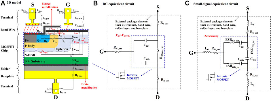
FIGURE 1. (A) Cross-section of a power MOSFET. (B) MOSFET DC equivalent circuit model. (C) MOSFET small-signal equivalent circuit model.
An ideal MOSFET chip can be equivalent to the constant and variable active devices, such as voltage-controlled current source, internal parasitic capacitances, internal parasitic series resistance, and anti-parallel body diode. The internal parasitic parameters include parasitic capacitances (drain-source capacitance CDS, gate-source capacitance CGS, and gate-drain capacitance CGD) and parasitic series resistances (drain-source resistance ESRDS_int, gate-source resistance ESRGS_int, and gate-drain resistance ESRGD_int). An additional equivalent series parasitic inductance may be included in the circuit. However, compared with the size of terminals and bond wires, the parasitic inductance of MOSFET is very small and can be ignored. The chip and external terminals are electrically interconnected through the aluminum bond wire packaging technology, which inevitably introduces the external packaging parasitic elements. 1) Parasitic inductances LS-ter, LG-ter, and LD-ter and parasitic resistances RS-ter, RG-ter, and RD-ter are generated from the gate, source, and drain terminals, respectively. 2) Parasitic inductances LS-BW, LG-BW and parasitic resistances RS-BW, RG-BW are generated from bond wires. 3) Parasitic resistances RD-solder and RD-base are generated from the solder and baseplate layers, respectively. The small-signal equivalent circuit model is simplified and the external parasitic inductances are combined into LG (LG-ter + LG-BW), LS (LS-ter + LS-BW), and LD (LD-ter) and the external parasitic resistances into RS_ext (RS-ter + RS-BW), RG_ext (RG-ter + RG-BW), and RD_ext (RD-solder + RD-base + RD-ter) to facilitate the analysis, as shown in Figure 1C.
2.2 Parasitic parameters as quality precursors
2.2.1 MOSFET quality states analysis with parasitic resistance
The MOSFET devices are typically packaged in discrete or power modules that provide heat dissipation and protection. The thermal mechanical stress caused by power loss and high thermal stress will accumulate in the die-attach layer, resulting in mechanical strain. If the strain exceeds the elastic region of the stress deformation characteristic, then cracks, voids, and material dislocations are produced in the die attach because of the great difference in the linear CTE of the materials (CTE for copper is 16–18, silicon is 2.6–3.3, and lead-free solder is 20–22.9 ppm/°C). From the existing literature study, RDS(on) is the most significant aging factor in MOSFETs [4, 11], [25–33]. Temperature elevation accelerates the degradation processes of semiconductor devices, and the Arrhenius equation can describe the influence of temperature. A relationship between the degradation rate D of RDS(on) and the average Tj of IGBTs can be described as [34]:
where C0 is an Arrhenius constant, Ea is the activation energy, and KB is a Boltzmann constant.
The degradation of RDS(on) should be a continuous process in a constant temperature accelerated aging test. Considering temperature changes as a function of time(t) in the aging process, the accumulated RDS(on) can be calculated as follows:
where RDS(on)_init is the initial RDS(on). The capacitor delta−connection can be converted into a star−connection, and the conversion method is shown in Figure 2A. The parasitic capacitances (CDS, CGS, and CGD) and the parasitic series resistances (ESRDS_int, ESRGS_int, and ESRGD_int) can be equivalent to a second-order RLC circuit composed of equivalent capacitances (CS, CG, and CD) and equivalent resistances (RS_int, RG_int, and RD_int) in series. Figure 2B shows a simplified MOSFET small-signal equivalent circuit in the form of capacitor star−connection, in which RS = RS_int + RS_ext, RG = RG_int + RG_ext, and RD = RD_int + RD_ext.
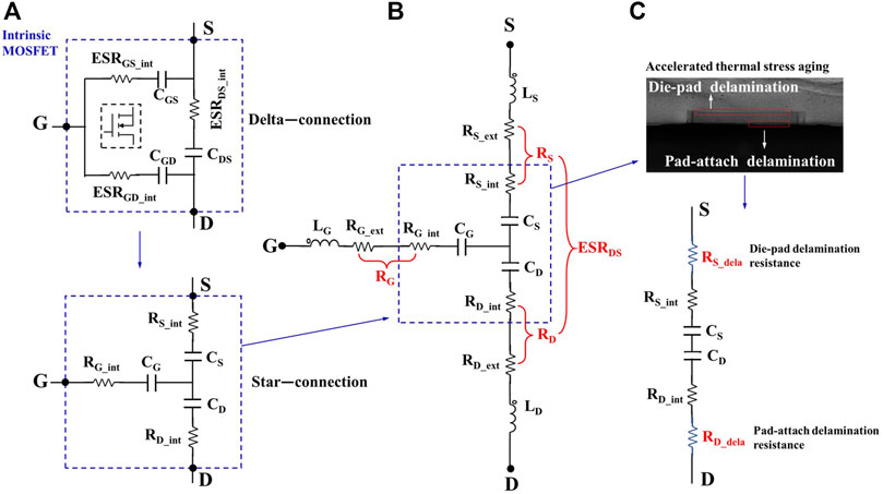
FIGURE 2. (A) Equivalent circuit of the parasitic capacitance (convert the capacitor delta connection to a star connection). (B) MOSFET small-signal equivalent circuit in the form of capacitor star connection. (C) Series resistances generated by bond−pad and pad−attach in the source-drain loop circuit.
RDS(ON) increases due to thermal overstress aging, and intermetallic growth and Kirkendall voids formation at the bond–pad and pad–attach interface at higher temperature. A simplified equivalent circuit for an aged power MOSFET is shown in Figure 2C, where the degradation of MOSFET can be equivalent to adding additional series resistance in the source–drain loop circuit, resulting in the increase of RDS(on) and ESRDS. A direct positive relationship between aging time and capacitor equivalent series resistance ESR was proposed in [35,36], that is, the ESR increase with aging. Similar phenomenon happens for the MOSFET because it has built in capacitors between gate and source as well as between gate and drain [37–39]. ESR(t)-based Physics-of-Failure (PoF) equations are provided as follows:
where ESRinit is the initial ESR; k(t) is the temperature-dependent degradation rate; k0 is the Arrhenius constant. The MOSFET drain-to-source equivalent series resistance (ESRDS) is associated with drain-to-source parasitic resistance (RD + RS) and can be described as follows:
where RD_init is the initial RD; RS_init is the initial RS; kD(t) and kS(t) are the temperature-dependent degradation rates of source and drain regions in MOSFET devices, respectively. We assume that the degradation rates of source and drain regions are the same in a constant temperature accelerated aging test. Eq. 5 can be modified as follows:
In general, in a normal measuring condition, RDS (on) as the key evaluating parameter of MOSFET quality states is affected easily by the changes in chip junction temperature, gate-source voltage VGS, and drain-source current ID. Therefore, a fine RDS(on) measurement requires high consistency of test conditions [31]. By contrast, the parasitic resistances (RS, RG, and RD) can be extracted with frequency domain reflectometry (FDR) technology without powering on the MOSFET [40,41]. Impressively, based on (2) and (6), RDS(on) (t) should show a similar exponential increasing trend as ESRDS(t). Then, a linear relationship between (RD + RS) (t) and RDS(on) (t) can be established, as follows:
where A and E are undetermined coefficients. The calculated value of RDS(on) can be easily obtained with (7), whereas the parasitic resistances (RD and RS) are extracted with FDR technology. Then, the quality level or/and quality states of MOSFET can be quantified quickly.
2.2.2 MOSFET bond wire fault analysis with parasitic inductance
Middle and high-power MOSFETs are generally based on wire-welded packaging, which uses some parallel aluminum bond wires to improve the current carrying capacity for electrical interconnection between source and terminal. Figure 3 depicts a typical power MOSFET in a TO−247 discrete package showing the equivalent circuit of each region from source to drain terminal. Multiple parallel bond wires are distributed at the source of MOSFET to jointly carry current, which makes it challenging to identify the damage of some bond wires directly. Therefore, our research focuses on the source bond wire faults. However, since only one bond wire is distributed at the gate, the fault is catastrophic and does not require significant attention. A problem that cannot be ignored is that the existence of bond wire introduces large parasitic inductance. A simple estimation is made in [42], the inductance is estimated as “1-mm length equivalent to 1-nH inductance.” In practice, 6 or 8 bond wires are usually used for interconnection. If the mutual inductance between parallel bond wires is ignored, then the total parasitic inductance of the bond wire can be simply calculated as L/(6 or 8). Figure 3 shows the RL equivalent circuit of a discrete MOSFET in the TO−247 package. Six parallel bond wires with different lengths exist between source and terminal, and each bond wire can be equivalent to a series circuit of resistance R and inductance L. LBW = L1//L2//L3//L4//L5//L6. Bond wire fault will reduce the number of parallel inductors in the RL equivalent circuit of the bond wire, increasing parasitic inductance LBW. Therefore, the change of parasitic inductance can be used to identify the health of the bond wire. In MOSFET small-signal equivalent circuit model (Figure 1C), the LBW is merged in LS. Thus, we can infer that LS will increase with the increasing severity of the number of bond wire lift-off. The detailed simulation and measurement process to extract parasitic inductances LS are reported in Section 3.3.
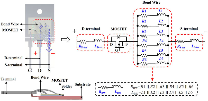
FIGURE 3. Simplified RL equivalent of a discrete MOSFET in TO−247 package.
2.2.3 Parasitic parameter extraction approach
In this study, the FDR measurement is used to extract the parasitic parameters of MOSFET [40,41]. This method is a two-port characterization approach that allows three terminals of a power device to be connected at a time with a vector network analyzer (VNA). No floating terminal error is observed during the measurement, which provides high measurement accuracy. The MOSFET small-signal equivalent circuit is shown in Figure 4, whereas the source terminal is connected to the VNA Port 1, the drain terminal is connected to the VNA Port 2, and the gate terminal is connected to the VNA ground. Each of the two-port network Z-parameters Z11, Z12, Z21, and Z22 can be equivalent to some second-order RLC circuits composed of independent inductances, capacitances, and resistances in series. Z11 is equivalent to the RS–RG–LS–LG–CS–CG series circuit, Z12 and Z21 are equivalent to the same RG–LG–CG series circuit, and Z22 is equivalent to the RD–RG–LD–LG–CD–CG series circuit. Notably, as a standard form of a two-port network, the equivalent capacitances (CG, CD, and CS) are star−connection in Figure 2B. The capacitor star−connection is converted to a delta−connection through (8)–(10) to extract the parasitic capacitances (CGS, CDS, and CGD). Figure 5A shows a typical impedance plot of a series RLC circuit, and the element values are L = 15 nH, C = 4 nF, and R = 1 Ω. The series RLC circuit impedance value can be expressed by (11), where w = 2πf and f is the frequency. The effect of capacitive reactance and resistance can be neglected at high frequency fHigh. The two-port network representation of the MOSFET can be simplified as Figure 5D, and L can be calculated using (12). At the self-resonance frequency fSRF, inductive reactance and capacitive reactance cancel each other, showing pure resistance characteristics. The two-port network representation of the MOSFET can be simplified as Figure 5C. The resistive components can be determined at the fSRF, and R is calculated from (13). According to the characteristics of a series self-resonance, the parasitic capacitance C can be obtained from (14).
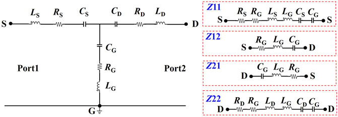
FIGURE 4. Two-port network representation of a MOSFET under zero biasing conditions.
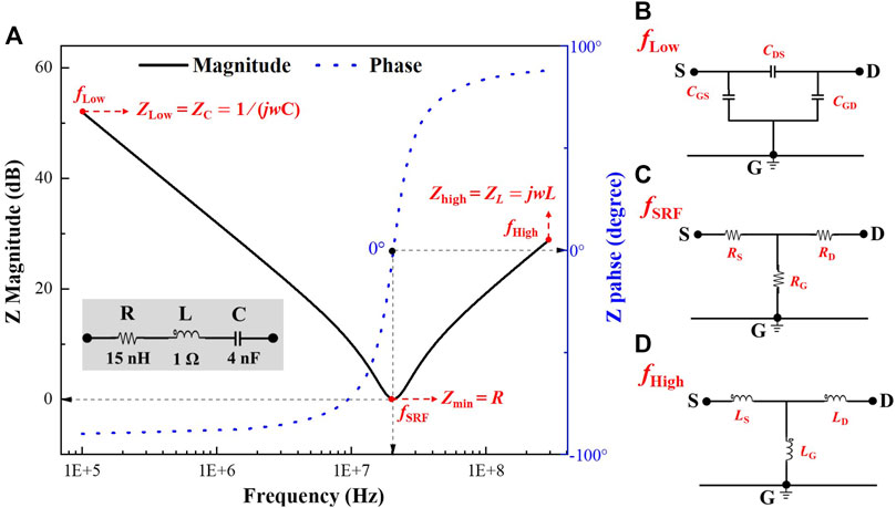
FIGURE 5. (A) Impedance magnitude and phase curve of series RLC circuit. (B) Two-port network representation of the MOSFET at low frequency fLow. (C) Two-port network representation of the MOSFET at the self-resonant frequency fSRF. (D) Two-port network representation of the MOSFET at high frequency fHigh.
Figure 6 shows the measuring principle of MOSFET two-port network and the VNA measurement system. To ensure the effective connection between MOSFET and VNA, we need to design a test fixture, which reserves three connection positions and ensures the low inductance connections between VNA and terminals. An effective test fixture needs to ensure 50 Ω impedance match on the transmission path and high isolation between input and output signals. The printed circuit board (PCB) test fixture composes two 50 Ω SMA adaptors, two 50 Ω microstrip lines, and a through-hole. The MOSFET is installed on the PCB test fixture and connected with VNA through SMA. The MOSFET source terminal is interconnected with VNA port 1, the MOSFET drain terminal is interconnected with VNA port 2, and the gate terminal is interconnected with the VNA ground through a PCB through-hole. De-embedding calibration is performed to remove the systematic errors caused by VNA itself, the test cables, adapters, and fixtures before scattering parameter (S-parameter) measurement. In this study, we use the 80502D calibration kit provided by Keysight for Short-Open-Load (SOL) to perform the VNA calibration. We also use PCB to design a new “Through” calibration element to extend the measurement plane to the device interface under the test (DUT) plane.
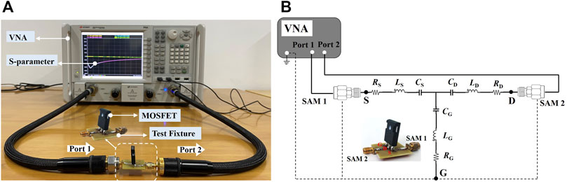
FIGURE 6. (A) Schematic diagram of the parasitic parameter two-port network extraction approach for a discrete MOSFET. (B) VNA measurement system, which is composed of one VNA, two test cables and the designed PCB test fixture.
2.2.4 Experimental setup
An accelerated aging test is conducted using power and thermal overstress. The RDS(on) and parasitic parameters of MOSFET at different aging times are extracted, and the quality level of MOSFET is quantified by establishing the numerical correlation model between them. The bond wire faults test is constructed by manually cutting off the bond wires. The parasitic parameters of MOSFET with various bond wire cut-off conditions are extracted, and the bond wire damage is quantified by establishing the numerical correlation model between parasitic parameters and the number of bond wires cut-off.
2.2.4.1 Aging
To determine how the parasitic resistance can effectively quantify the quality level of MOSFET power devices, an accelerated aging experimental platform, and the RDS(on) test platform are set up. Figure 7 depicts the schematic of the accelerated aging setup. The DUT, shown in Figure 7B, is placed in an accelerated aging station to stress it electrically and thermally. The simultaneous stress is achieved by current flow and thermal during the on-state of the DUT. Figure 8 shows the schematic of the RDS(on) test setup. Multiple MOSFETs are aged for different times and are characterized by the RDS(on) test system and the two-port measurement system. A data acquisition system is used to collect the drain-to-source voltage VDS and the drain-source current ID to calculate RDS(on). A k-type thermocouple is attached to the surface of the MOSFET baseplate to measure the temperature during the accelerated aging in real-time, which is used to feedback and adjust the load current ID. A liquid cooling system is used to keep the chip junction temperature stable during RDS(on) extraction after accelerated aging. The test steps are as follows:
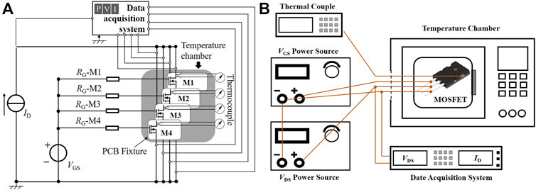
FIGURE 7. (A) Schematic of the accelerated aging experimental and (B) accelerated aging setup for MOSFET.
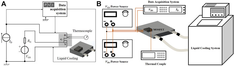
FIGURE 8. (A) Schematic of the RDS(on) test system and (B) RDS(on) test setup for MOSFET.
Step 1:. Extract the MOSFET RDS(on) at the desired conditions;
Step 2:. Measure the S-parameters over a frequency range of 10–300 MHz, as shown in Figure 6;
Step 3:. Convert the measured S-parameters to Z-parameters to calculate the parasitic parameters;
Step 4:. Age the MOSFETs according to the above requirements;
Step 5:. Repeat steps 1–4.
2.2.4.2 Bond wire fault
To reduce the experimental time, the approach of shearing off bond wires is demonstrated to simulate the fatigue of bond wires. In this study, a 1000 V N- channel power MOSFET in a TO−247 package (IXFK32N100P) is used to analyze the correctness of LS as the precursor to identifying bond wire fault. First, we use laser equipment to remove the epoxy layer of MOSFET to expose the bond wire completely. Then, the bond wire faults are simulated by manually cutting off the bond wires individually, and the LS is extracted by using the two-port S-parameter measurement system. The implementation steps are as follows:
Step 1:. Remove the EMC with a laser device to expose the bond wires;
Step 2:. Measure the S-parameters over a frequency range of 10–300 MHz;
Step 3:. Convert the measured S-parameters to Z-parameters and calculate the initial parasitic inductance LS;
Step 4:. Cut off the bond wire to make a damage model;
Step 5:. Repeat steps 2–4 until only one bond wire is left for the interconnection between the source and drain of the MOSFET.
3 Experimental results and discussion
3.1 Validation parasitic parameter extraction for MOSFET in TO-247
In this paper, a 400V N-Channel discrete MOSFET (IRFP340) in a TO−247 package is used to verify the two-port measurement technique. The values of Z11, Z12, Z21, and Z22 can be calculated using Eqs 15–17 based on the two-port network. At a high frequency fHigh, the contribution of capacitance and resistance to the RLC circuit impedance can be ignored, whereas the high-frequency impedance can be equal to the inductive reactance. Individual inductances LS, LG, and LD can be extracted through Eqs 18–20. At the fSRF, the contribution of capacitance and inductance to the RLC circuit impedance can be neglected. Individual resistances RS, RG, and RD can be extracted using Eqs 21–23. The individual capacitances CS, CG, and CD are obtained by plugging in the extracted LS, LG, and LD to the fSRF expression Eq. 14, respectively. Finally, the capacitor star−connection is converted to a delta−connection to extract CGS, CGD, and CDS through Eqs 8–10. First, the S−parameter of the MOSFET was obtained from VNA measurement and converted into Z−parameters. Then, the parasitic inductances, capacitances, and resistances were accurately calculated from Z−parameters. After extracting the parasitic parameters, we also plug these values back into the established MOSFET two-port network model (as shown in Figure 4) for Advanced Design System (ADS) circuit simulation to verify the small-signal equivalent circuit and the general parasitic parameters extraction methodology. Figure 9 shows the frequency response curves of the Z-parameters obtained from ADS simulation and VNA experimental measurement. The ADS simulation curve (red dashed line) is in good agreement with the experimental value (black solid line), which validates the mathematical formulas and extraction approach mentioned in Section 2.2.3. In addition, the secondary validation approach is realized by comparing the extracted inductances from the proposed VNA measurement at the fHigh with the MOSFET datasheet values. The parasitic inductances LS and LD obtained from the proposed two-port extraction technique are 12.358 and 5.262 nH, respectively. Considering the unavoidable measurement error, the extracted capacitances are consistent with the datasheet values (LD = 5 nH, LS = 13 nH, 6 mm from package and center of die contact), and the mismatch is 4.94% and 5.24%, respectively. The experimental results show that the proposed two-port network methodology is suitable for accurately extracting the parasitic parameters of discrete power MOSFETs.
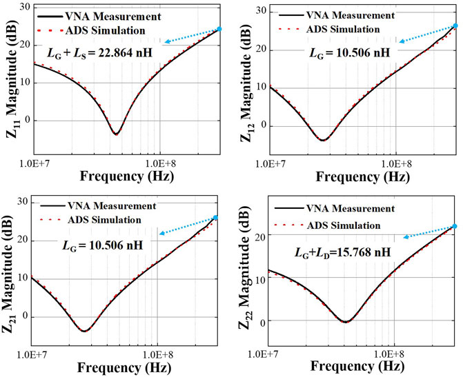
FIGURE 9. Z-parameters obtained from VNA experimental measurement and ADS simulation.
3.2 Quality level estimation of MOSFET
The IRFP340 N-Channel MOSFETs are installed on the PCB fixture and then placed in a temperature chamber at 100°C to perform aging. A 15 V DC gate-source voltage VGS [>VGS(TH)] is applied across the G–S terminals to turn on the MOSFETs fully, and a constant drain-source current ID = 1.65 A is applied across the D–S terminals to generate sustained power stress during the accelerated aging procedure (Figure 7). The baseplate temperature of MOSFET reaches 190°C within 10 min, which is stabilized at (210 ± 2) °C, and the power loss is ≈5.14 W during the entire accelerated aging process. RDS and parasitic parameters of the MOSFET are extracted as a reference before aging, the initial RDS(on) is approximately equal to 0.4023 Ω. A liquid cooling system is used to adjust the heat dissipation to keep the baseplate temperature of the MOSFET at (25 ± 0.1) °C, to ensure the stability of the chip junction temperature during the RDS(on) test. The VGS is set to 10 V according to the test requirements from the datasheet, and the ID is selected as 2.0 A while taking the measurements of RDS(on) using the data acquisition system.
Usually, MOSFETs are remarkably stable for a period before rapid degradation. The degradation process of RDS(on) is divided into two stages: the delay stage and the degradation stage. Like the results of the degradation of the formula (1), the RDS(on) variation is found to be exponential to a certain value. Table 1 summarizes the RDS(on) and parasitic parameters extracted at different aging times. Aged for 10 h, RDS(on) remains almost unchanged, indicating that the MOSFET is in the stable stage. When the cumulative aged time is 20 h, RDS(on) increases by 38.30 mΩ, indicating that the MOSFET is degraded. Therefore, the duration aged time is adjusted to 5 h to control the degradation speed of the MOSFET. The cumulative values of RD + RS and RDS(on) are highly consistent with the increase of aged time, as shown in Figure 10B, which conforms the assumption of (7). Meanwhile, RD + RS and RDS(on) have a quasi-linear positive correlation, this finding is consistent with our theoretical analysis in Section 2.2.1 However, the calculated change rate of RD + RS is 5%–6% higher than that of RDS(on) at different aging time. Since RD + RS is a newly proposed precursor, more studies are needed to support it to become an acceptable standard for quantifying the aging degree of MOSFETs. In the power electronics industry, RDS(on) has been widely accepted as a general evaluation standard for qualifying MOSFETs’ aging level. To visually describe the degradation degree of MOSFETs, RDS(on) can be quickly predicted through the fitting relationship between RD + RS and RDS(on).
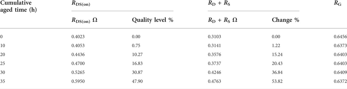
TABLE 1. RDS(on) and parasitic resistances at different aged time.
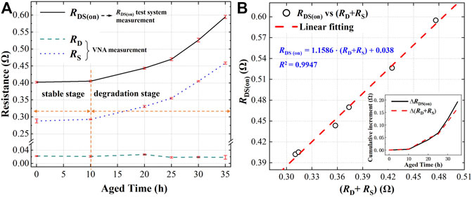
FIGURE 10. (A) Measured RDS(on), RD, and RS of MOSFET at different aging times (RDS(on) is measured by RDS (on) test system, RD and RS are extracted from the VNA measurement). (B) Relationship between RDS(on) and RD + RS.
For power MOSFETs, the failure threshold can be considered as a 25% increase in RDS(on) relative to its initial value. The RDS(on) change ratio can be used to measure the approximate quality level of MOSFETs, quality level = |aged RDS(on)—RDS(on)_init|/RDS(on)_init]. The quality level in the case of those aged 30 h is 30.87%, which is more than 25%. Figure 10B is drawn by using the data summarized in Table 1. It shows the relationship between RDS(on) and RD + RS values. This relationship can be quantified by using the basic fitting tool in MATLAB, as shown in (24).
Once the initial RDS(on) and corresponding RD + RS are known, the predicted RDS(on) and approximate quality level after accelerated aging can be easily determined from the RD + RS. Six new IRFP–340 MOSFETs (i.e., M1, M2, M3, M4, M5, and M6) are aged for different time durations using power and thermal overstress in a controlled environment to verify the accuracy of the fitting function (24) by applying similar stress. The RDS(on) of MOSFET M1 to M6 may be predicted by (24) using the RD + RS values measured by VNA. A 1.92 A constant current ID is applied across the drain-source terminals for extremely accelerated aging of the MOSFET, whereas the ambient temperature is 100°C. The power dissipation across each MOSFET is ≈6.97 W, and the baseplate temperature is stabilized at (235 ± 2) °C during the extremely accelerated aging procedure. M1, M2, M3, M4, M5, and M6 are aged according to the aging mentioned above process, including M1 aged for 10 h, M2 aged for 20 h, M3 aged for 30 h, M4 aged for 40 h, M5 aged for 50 h, and M6 aged for 60 h. Table 2 presents the measured RDS(on) values, measured RD + RS, RDS(on) values predicted using (24), and quality level. Owing to the sharp increment in RDS(on) of M6, the RD + RS is significantly larger than other MOSFETs, and the quality level exceeds 100%. Therefore, this MOSFET can be considered damaged. The predicted RDS(on) of all MOSFETs except M6 is nearly equal to the actual measured RDS(on) value, whereas the maximum error percentage between them is less than 2%. The maximum error percentage of the predicted and the measured quality level is less than 3%, giving us sufficient confidence in our proposed quality level quantification approach. However, in the case of M6, the predicted accuracy of (24) has a small deviation. The error between the actual measured RDS(on) and the predicted RDS(on) is 3.63%, and the error between the actual and predicted quality levels is 9.84%. Extreme thermal stress forces M6 to degrade seriously, resulting in very high RDS(on) (>3 × initial RDS(on)), which makes it difficult to accurately control the chip junction temperature, so the measured value of RDS will also have errors. However, although a mismatch exists between the predicted quality level and the actual measured quality level of M6, the serious degradation damage of the MOSFET can still be identified based on RD + RS. Compared with the RDS(on) precursor parameter highly dependent on Tj, Vgs, and ID, the parasitic resistance without MOSFET power on the test proposed by us has better advantages in quantifying the quality level.
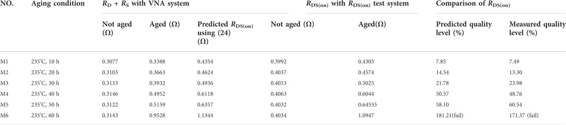
TABLE 2. Comparison between predicted RDS (on) using (24) and measured RDS (on).
Figure 11 shows X-ray and C-SAM graphs of the four MOSFETs with different extremely aging times. In the X-ray photographs of M1−M4, the delamination regions are marked with red rectangles. From the X-ray image, the delamination of M1 and M2 only occurs between the source metal layer and epoxy layer, whereas the delamination of M2 is more evident. With the increase of extremely accelerated aging time, in M3 and M4, delamination occurs between the source metal layer and epoxy layer and between the drain metal layer and the solder layer. A slight “bulge” is observed on the top of M4, where the die is located, indicating that the epoxy layer is seriously separated from the die. Then, the die area is observed with C-SAM images. The yellow and red spots accompanied by the unexpected frequency responses observed on the surfaces indicate of delamination. Evidently, the yellow and red regions in M1–M4 increase, in turn, indicating that extremely accelerated thermal aging effectively forces the degradation of MOSFETs.
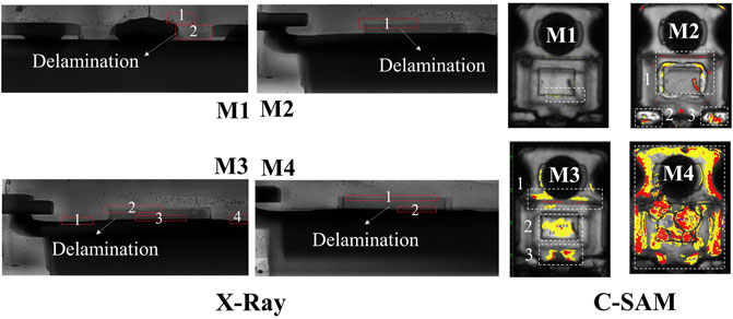
FIGURE 11. X-ray and SAM graphs of MOSFETs.
In summary, the impedance magnitude of MOSFET at the fSRF carries the available and critical information strongly related to aging degradation. Using the linear fitting formula between RD + RS and RDS(on), the quality level in MOSFET can be quickly identified by comparing the percentage change between predicted RDS(on) and initial RDS (on). This finding is a novel discovery, providing an effective quality screening technology for power semiconductor devices without power on treatment.
3.3 Bond wire fault quantitative assessment of MOSFET
Middle- and high-power MOSFETs generally use some parallel aluminum bond wires for the electrical path between the chip and the source terminal. For IXFK32N100P 1000V 32A N-channel MOSFET considered, for instance, six parallel bond wires with a diameter of 0.279 mm exist between the source-electric and source-terminal. Figure 12 shows the internal structure of IXFK-32N100P and the serial number marked on each bond wire. The damage model is established by cutting off the bond wire, including one bond wire fault (cut off No. 1), two bond wires fault (cut off No. 1 and No. 2), three bond wires fault (cut off No. 1, No. 2, and No. 3), four bond wires fault (cut off No. 1, No. 2, No. 3, and No. 4) and five bond wires fault (cut off No. 1, No. 2, No. 3, No. 4, and No. 5).
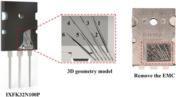
FIGURE 12. Internal structure of the MOSFET, whereas each bond wire is marked with serial number.
The position of six bond wire pads on the die and six pads on the source terminal is extracted from a dissembled package. The 3D geometry model of the MOSFET power device is established based on the actual size mapping, and the damage model is defined by cutting off the bond wires one by one. Then, the 3D model is imported into the Q3D-extractor finite element software to calculate the inductance of the commutation loop defined by the current path between the chip source and the source terminal. Figure 13 shows the source inductance LSource-BW with different amounts of bond wires cut-off. This indicates that an approximately positive correlation exists between the number of bond wire faults and LSource-BW. When one or two bond wires are cut-off, the percentage change of LSource-BW is close to 1.46% and 7.09%, respectively. Even the slight degradation of the bond wire can still show high sensitivity. These results indicate that the proposed bond wire damage detection approach is reasonable.
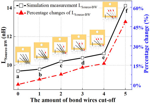
FIGURE 13. LSource-BW at different amounts of bond wires cut-off. a = 9.59 nH, b = 9.73 nH, c = 10.27 nH, d = 10.52 nH, e = 10.82 nH, f = 14.17 nH.
In the MOSFET small signal-equivalent circuit model (Figure 1), the parasitic inductance of the source generated by bond wires is combined into LS. Therefore, theoretically, the lift-off of source bond wires will directly and evidently cause the change of LS. Figure 14 shows the Z-parameter frequency response curves of different bond wire faults. At high frequency fHigh, Z11 (Z11_High = LS + LG) increases significantly with the number of bond wires cut off, but Z12 (Z12_High = LG), Z21 (Z21_High = LG), and Z22 (Z22_High = LG + LD) are almost unchanged. This case indicates that the parasitic inductance of the source rises with the increase of the number of bond wires cut-off, which is reflected in the increase of LS. The ratios expressed as percentage change are calculated to define the degree of bond wire degradation. Percentage changes of Z11 and LS are the different ratios of the measured value with the actual device compared with the initial value of the fault-free DUT. At 300 MHz, the percentage change in Z11-parameters of each model is close to 1.90%, 4.04%, 6.66%, 8.67%, and 23.70%, respectively.
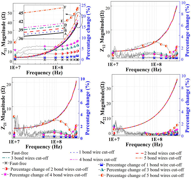
FIGURE 14. Z-parameters of IXFK32N100P MOSFET with different numbers of bond wire cut−off. (A = 37.24 Ω, B = 37.95 Ω, C = 38.74 Ω, D = 39.72 Ω, E = 40.47 Ω, F = 46.06 Ω).
Figure 15 indicates that the LS has an increment with the degradation of bond wires, which has the same change trend as the LSource-BW obtained by finite element analysis, and the offset is less than 0.5 nH. This finding further verifies the correctness of LS extracted approach from the proposed two-port network measurement and the feasibility of LS as a precursor. For ease of description, we define that 1 or 2 bond wires lift-off can be regarded as “slight fault,” and 3, 4, or 5 bond wires lift-off is “serious fault.” When 1 or 2 bond wires fail, LS increases from 9.19 to 9.55 and 9.91 nH, 3.99% and 7.87% higher than the initial value, respectively. Notably, in the case of “slight fault,” LS shows sensitive changes and has good identifiability. This case means that the proposed approach can distinguish a slight fault with high discrimination. In the case of “serious fault,” LS increases sharply, and the percentage changes of LS are 13.25%, 16.29%, and 48.71%, respectively. Therefore, regardless of a “slight fault” or “serious fault,” the source parasitic inductance has a high resolution as a precursor for bond wire damage detection. In conclusion, at high frequency, LS is very sensitive to the fault of the bond wire, which provides a theoretical basis for establishing a novel bond wire reliability screening technology.
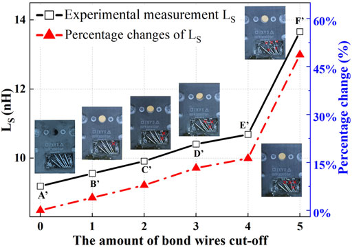
FIGURE 15. LS at different numbers of bond wire cut−off. A’ = 9.19 nH, B’ = 9.55 nH, C’ = 9.91 nH, D’ = 10.41 nH, E’ = 10.69 nH, F’ = 13.66 nH.
4 Conclusion
A novel failure quantitative assessment approach to MOSFET power device by detecting parasitic parameters is proposed in this study. The experimental results indicate that source-drain parasitic resistance increases with the increasing quality level and illustrates a quasi-linear positive correlation with RDS(on) in an error of less than 3%. Meanwhile, LS increases with the fault number of bond wires. It has high sensitivity and can show a satisfactory recognition even for slight faults. Therefore, the aging degradation level (metallization reconstruction and die-attach solder delamination) and bond wire failure degree can be quantified by detecting the source-drain parasitic resistance and the source parasitic inductance, respectively.
WBG power devices are also packaged via wire-welding packaging process. Hence, the packaging failure are always caused by the solder layer degradation and bond wire failure. Since the junction capacitance of the WBG power device is smaller, it has a high fSRF. Skin effect forces the increase in parasitic resistance of the conductors, so the source-drain parasitic resistance of the WBG power device is larger than that of the silicon power device. Theoretically, the proposed approach has higher recognition resolution when applied to WBG power devices.
Impressively, parasitic parameters can be obtained through domain measurement technology without turning on MOSFETs. Compared with the degradation precursors-based methods, the proposed approach can effectively avoid the influence of chip self-heating and external loading test parameters (such as source-drain current, gate-source voltage, and others) on testing results and is suitable for rapid quality screening of power devices. Moreover, the proposed approach can quantify the actual aging degree of the power devices compared with the morphology characteristics-based methods and quickly predict the type of package failure by identifying the changes of parasitic parameters in a single measurement. Providing an effective quality screening way for power devices and raising an on-line quality monitoring technology for the manufacturing process are promising [42].
Data availability statement
The original contributions presented in the study are included in the article/supplementary material, further inquiries can be directed to the corresponding authors.
Author contributions
MY: Conceptualization, Data curation, Investigation, Methodology, Original draft. DY: Investigation, Review, Supervision, and editing. SH: Investigation, Methodology, and editing. MC: Conceptualization, Investigation, Methodology, and editing. JX: Methodology, Review, and Funding acquisition. KZ: Data curation; G-QZ: Investigation, Methodology, and Guidance.
Funding
This research was supported by the Innovation-Driven Development Project of Guangxi Province under No. GuiKeAA21077015, the Key R&D Plan Project of Guangxi Province under No. GuiKe AB20159038, the National Natural Science Foundation of China under No.62264003 and No. 62164004, the Science and Technology Planning Project of Guangxi under No. GuiKe AD20297022, the Science and Technology Program of Guangxi under No. AB20159007, the Postdoctoral Science Foundation of China under No.2020M683625XB, the Science Research and Technology Development Program of Guilin under No. 20200103-2, No. 20210210-2, and No. 20210205-4, and the Innovation Project of GUET Graduate Education under No.2021YCXB01.
Conflict of interest
The authors declare that the research was conducted in the absence of any commercial or financial relationships that could be construed as a potential conflict of interest.
Publisher’s note
All claims expressed in this article are solely those of the authors and do not necessarily represent those of their affiliated organizations, or those of the publisher, the editors and the reviewers. Any product that may be evaluated in this article, or claim that may be made by its manufacturer, is not guaranteed or endorsed by the publisher.
References
1. Yang S, Bryant A, Mawby P, Xiang D, Ran L, Tavner P. An industry-based survey of reliability in power electronic converters. IEEE Trans Ind Appl (2011) 47(3):1441–51. doi:10.1109/TIA.2011.2124436
2. Rodriguez MA, Claudio A, Theilliol D, Vela LG. A new fault detection technique for IGBT based on gate voltage monitoring. In: Proceeding of the 2007 IEEE Power Electronics Specialists Conference; June 2007; Orlando, FL, USA. IEEE (2007). p. 1001–5. doi:10.1109/PESC.2007.4342127
3. Fischer K, Pelka K, Bartschat A, Tegtmeier B, Coronado D, Broer C, et al. Reliability of power converters in wind turbines: Exploratory analysis of failure and operating data from a worldwide turbine fleet. IEEE Trans Power Electron (2019) 34(7):6332–44. doi:10.1109/TPEL.2018.2875005
4. Abuelnaga MN, Bahman AS. A review on IGBT module failure modes and lifetime testing. IEEE Access (2021) 9:9643–63. doi:10.1109/ACCESS.2021.3049738
5. Choi UM, Blaabjerg F, Jørgensen S, Iannuzzo F, Wang H, Uhrenfeldt C, et al. Power cycling test and failure analysis of molded intelligent power IGBT module under different temperature swing durations. Microelectronics Reliability (2016) 64:403–8. doi:10.1016/j.microrel.2016.07.020
6. Choi UM, Blaabjerg F, Lee KB. Study and handling methods of power IGBT Module failures in power electronic converter systems. IEEE Trans Power Electron (2015) 30(5):2517–33. doi:10.1109/TPEL.2014.2373390
7. Chen C, Pickert V, Al-Greer M, Jia C, Ng C. Localization and detection of bond wire faults in multichip IGBT power modules. IEEE Trans Power Electron (2020) 35(8):7804–15. doi:10.1109/TPEL.2020.2965019
8. Choi UM, Blaabjerg F, Jørgensen S. Power cycling test methods for reliability assessment of power device modules in respect to temperature stress. IEEE Trans Power Electron (2018) 33(3):2531–51. doi:10.1109/TPEL.2017.2690500
9. Mandeya R, Chen C, Pickert V, Naayagi RT, Ji B. Gate–emitter pre-threshold voltage as a health-sensitive parameter for IGBT chip failure monitoring in high-voltage multichip IGBT power modules. IEEE Trans Power Electron (2019) 34(9):9158–69. doi:10.1109/TPEL.2018.2884276
10. Weckbrodt J, Ginot N, Batard C, Azzopardi S. Monitoring of gate leakage current on SiC power MOSFETs: An estimation method for smart gate drivers. IEEE Trans Power Electron (2021) 36(8):8752–60. doi:10.1109/TPEL.2021.3056648
11. Halick M, Sathik M, King Jet T, Sundarajan P. Online computation of IGBT on-state resistance for off-shelf three-phase two-level power converter systems. Microelectronics Reliability (2016) 64(2):379–86. doi:10.1016/j.microrel.2016.07.067
12. Oukaour A, Tala-Ighil B, Pouderoux B, Tounsi M, Bouarroudj-Berkani M, Lefebvre S, et al. Ageing defect detection on IGBT power modules by artificial training methods based on pattern recognition. Microelectronics Reliability (2011) 51(2):386–91. doi:10.1016/j.microrel.2010.08.006
13. Gonzalez-Hernando F, San-Sebastian J, Garcia-Bediaga A, Arias M, Iannuzzo F, Blaabjerg F. Wear-out condition monitoring of IGBT and mosfet power modules in inverter operation. IEEE Trans Ind Appl (2019) 55(6):6184–92. doi:10.1109/TIA.2019.2935985
14. Passmore LJ, Awadelkarim OO, Cusumano JP. High-sensitivity tracking of MOSFET damage using dynamic-mode transient measurements. IEEE Trans Instrum Meas (2010) 59(6):1734–42. doi:10.1109/TIM.2009.2028213
15. Sun P, Gong C, Du X, Luo Q, Wang H, Zhou L. Online condition monitoring for both IGBT module and DC-Link capacitor of power converter based on short-circuit current simultaneously. IEEE Trans Ind Electron (2017) 64(5):3662–71. doi:10.1109/TIE.2017.2652372
16. Shao L, Xu G, Li P. A hybrid model of turn-off loss and turn-off time for junction temperature extraction. IEEE J Electron Devices Soc (2022) 10:3–12. doi:10.1109/JEDS.2021.3125829
17. Górecki K, Górecki P, Zarebski J. Measurements of parameters of the thermal model of the IGBT module. IEEE Trans Instrum Meas (2019) 68(12):4864–75. doi:10.1109/TIM.2019.2900144
18. Ji B, Song X, Cao W, Pickert V, Hu Y, Mackersie J, et al. In-situ diagnostics and prognostics of solder fatigue in IGBT modules for electric vehicle drives. IEEE Trans Power Electron (2015) 30(3):1535–43. doi:10.1109/TPEL.2014.2318991
19. Li K, Tian GY, Cheng L, Yin A, Cao W, Crichton S. State detection of bond wires in IGBT modules using eddy current pulsed thermography. IEEE Trans Power Electron (2014) 29(9):5000–9. doi:10.1109/TPEL.2013.2288334
20. Baker N, Dupont L, Munk-Nielsen S, Iannuzzo F, Liserre M. IR camera validation of IGBT junction temperature measurement via peak gate current. IEEE Trans Power Electron (2017) 32(4):3099–111. doi:10.1109/TPEL.2016.2573761
21. Zhang J, Du X, Wu Y, Luo Q, Sun P, Tai H. Thermal parameter monitoring of IGBT module using case temperature. IEEE Trans Power Electron (2018) 34(8):7942–56. doi:10.1109/tpel.2018.2879825
22. Dreher P, Schmidt R, Vetter A, Heppb J, Karl A, Brabec CJ. Non-destructive imaging of defects in Ag-sinter die attach layers–A comparative study including X-ray, scanning acoustic microscopy and thermography. Microelectronics Reliability (2018) 88(90):365–70. doi:10.1016/j.microrel.2018.07.121
23. Feng W, Meng Q, Xie Y, Fan H. Wire bonding quality monitoring via refining process of electrical signal from ultrasonic generator. Mech Syst Signal Process (2011) 25(3):884–900. doi:10.1016/j.ymssp.2010.09.010
24. Hanif A, Wasekul Azad ANM, Khan F. Detection of bond wire lift off in IGBT power modules using ultrasound resonators. In: Proceeding of the 2020 IEEE Appl. Power Electron. Conf. Expo.; March 2020; New Orleans, LA, USA. IEEE (2020). p. 345–50. doi:10.1109/APEC39645.2020.9124226
25. Azoui T, Tounsi P, Dupuy P, Dorkel JM, Martineau D. Numerical and experimental results correlation during power MOSFET ageing. In: Proceeding of the 13th Int. Conf. Therm., Mech. Multi-Phys. Simul. Exp. Microelectron. Microsyst.; April 2012; Cascais, Portugal. IEEE (2012). p. 1/4–/4. doi:10.1109/ESimE.2012.6191798
26. Eleffendi MA, Johnson CM. In-service diagnostics for wire-bond lift-off and solder fatigue of power semiconductor packages. IEEE Trans Power Electron (2017) 32(9):7187–98. doi:10.1109/TPEL.2016.2628705
27. Khera N, Khan SA. Prognostics of power MOSFET using artificial neural network approach. J Electr Eng Technol (2019) l5(1):487–99. doi:10.1007/s42835-019-00272-0
28. Celaya JR, Saxena A, Kulkarni CS, Saha S, Goebel K. Prognostics approach for power MOSFET under thermal-stress aging. In: Proceeding of the 2012 Annu. Reliab. Maintainability Symp.; January 2012; Reno, NV, USA. IEEE (2012). p. 1–6. doi:10.1109/RAMS.2012.6175487
29. Cheng T, Lu DDC, Siwakoti YP. A MOSFET SPICE model with integrated electro-thermal averaged modeling, aging, and lifetime estimation. IEEE Access (2021) 9:5545–54. doi:10.1109/ACCESS.2020.3047110
30. Dusmez S, Akin B. An accelerated thermal aging platform to monitor fault precursor on-state resistance. In: Proceeding of the 2015 IEEE Int. Electr. Mach. Drives Conf.; May 2015; Coeur d’Alene, ID, USA. IEEE (2015). p. 1352–8. doi:10.1109/IEMDC.2015.7409238
31. Testa SDC, Russo S. A reliability model for power MOSFETs working in avalanche mode based on an experimental temperature distribution analysis. IEEE Trans Power Electron (2012) 27(6):3093–100. doi:10.1109/TPEL.2011.2177279
32. Pu S, Yang F, Vankayalapati BT, Ugur E, Xu C, Akin B. A practical on-board SiC MOSFET condition monitoring technique for aging detection. IEEE Trans Ind Appl (2020) 56(3):2828–39. doi:10.1109/TIA.2020.2980220
33. Qin F, Bie X, An T, Dai J, Dai Y, Chen P. A lifetime prediction method for IGBT modules considering the self-accelerating effect of bond wire damage. IEEE J Emerg Sel Top Power Electron (2021) 9(2):2271–84. doi:10.1109/JESTPE.2020.2992311
34. F , Cai X, Zhu R, Deng HQ, Liu C, Cai X, et al. Capacitor ESR and C monitoring in modular multilevel converters. IEEE Trans Power Electron (2020) 35(4):4063–75. doi:10.1109/TPEL.2019.2939185
35. Sun B, Fan X, Qian C, Zhang GQ. PoF-simulation-assisted reliability prediction for electrolytic capacitor in LED drivers. IEEE Trans Ind Electron (2016) 63(11):6726–35. doi:10.1109/TIE.2016.2581156
36. Hanif A, Roy S, Khan F. Detection of gate oxide and channel degradation in SiC power MOSFETs using reflectometry. In: Proceeding of the 2017 IEEE Workshop Wide Bandgap Power Devices Appl.; October 2017; Albuquerque, NM, USA. IEEE (2017). p. 383–7. doi:10.1109/WiPDA.2017.8170577
37. Nasrin MS, Khan FH, Alam MK. Quantifying device degradation in live power converters using SSTDR assisted impedance matrix. IEEE Trans Power Electron (2014) 29(6):3116–31. doi:10.1109/TPEL.2013.2273556
38. Hanif A, DeVoto D, Khan F. Bond wire damage detection and SOH estimation of a Dual-Pack IGBT power module using active power cycling and reflectometry. IEEE Trans Power Electron (2020) 35(7):6761–72. doi:10.1109/TPEL.2019.2958898
39. Liu T, Feng Y, Ning R, Wong TTY, Shen ZJ. Extracting parasitic inductances of IGBT power modules with two-port S-parameter measurement. In: Proceeding of the 2017 IEEE Transp. Electrif. Conf. Expo.; June 2017; Chicago, IL. IEEE (2017). p. 281–7. doi:10.1109/ITEC.2017.7993285
40. Liu T, Wong TTY, Shen ZJ. A new characterization technique for extracting parasitic inductances of SiC power MOSFETs in discrete and module packages based on two-port S-parameters measurement. IEEE Trans Power Electron (2018) 33(11):9819–33. doi:10.1109/TPEL.2017.2789240
41. Lee W, Pak JS, Pak J, Ryu C, Park J, Kim J. A frequency tunable resonant clock distribution scheme using bond-wire inductor. In: Proceeding of the 2008 IEEE Electr. Des. Adv. Packag. Syst. Symp.; December 2008; Seoul, Korea (South). IEEE (2008). p. 24–6. doi:10.1109/EDAPS.2008.4735989
Keywords: MOSFETs, quantitative assessment, parasitic parameters, quality level, bond wire fault, detection
Citation: Yun M, Yang D, He S, Cai M, Xiao J, Zhang K and Zhang G-Q (2022) Failure quantitative assessment approach to MOSFET power device by detecting parasitic parameters. Front. Phys. 10:1050678. doi: 10.3389/fphy.2022.1050678
Received: 22 September 2022; Accepted: 30 September 2022;
Published: 17 October 2022.
Edited by:
Ye Yuan, Songshan Lake Material Laboratory, ChinaReviewed by:
Zhang Siyuan, Qinghai Institute of Salt Lakes (CAS), ChinaJing Li, South China University of Technology, China
Copyright © 2022 Yun, Yang, He, Cai, Xiao, Zhang and Zhang. This is an open-access article distributed under the terms of the Creative Commons Attribution License (CC BY). The use, distribution or reproduction in other forums is permitted, provided the original author(s) and the copyright owner(s) are credited and that the original publication in this journal is cited, in accordance with accepted academic practice. No use, distribution or reproduction is permitted which does not comply with these terms.
*Correspondence: Daoguo Yang, daoguo_yang@163.com; Siliang He, siliang_he@guet.edu.cn