 M. C. Paliwoda
 E. M. Tejero
 G. R. Gatling
- U.S. Naval Research Laboratory, Washington, DC, United States
For two dipole antennas in a two-port system, an impedance calibration method is presented for situations where the dipole antennas are inaccessible during testing, but environmental changes require recalibration, such as during mutual-impedance measurements of a plasma inside a vacuum chamber. The antenna system of this study is composed of two dipoles connected by rigid coax cables to their respective calibration boxes. The boxes house surface mounted baluns, for balancing the dipoles, and surface mounted standards, for calibrating the cables. The cables connect the system through the chamber walls to the measurement hardware, a Vector Network Analyzer (VNA). The measured S-parameters are simulated in the python package scikit-rf to de-embed the dipoles. This new virtual approach incorporates the balun common mode and eliminates error from the conventional balun characterization where only the differential mode is considered. The presented calibration method has been validated with direct measurements of known cable loads and a COMSOL simulation for a range of 1 MHz–1 GHz, equating to an electron density range of roughly
1 Introduction
A plasma mutual impedance probe is a diagnostic that measures plasma parameters, such as electron density and electron temperature, by fitting a plasma impedance model to the real and imaginary components of the mutual impedance (Storey et al., 1998a). The mutual impedance probe is composed of two antennas that measure the frequency response of a signal transmitted through the plasma. Although, the calibration of two antennas has established methods in the electrical engineering discipline (C63.5, 2017), this work accounts for laboratory plasma testing conducted in vacuum chambers, where bending cables attached to translation stages and changing cable temperatures due to plasma sources, will change the calibration along a coaxial cable.
Storey et al. (1969), Storey et al. (1998a), Storey et al. (1998b) first adapted the mutual impedance method from its geophysics origin to measure characteristic resonance frequencies of a cold unmagnetized and magnetized plasma. Pottelette et al. (1975) adapted the theory for a dipole configuration and a warm isotropic plasma. Chasseriaux et al. (1972) and Debrie et al. (1976) independently validated the measurement of electron density and electron temperature. Grard (1997) expanded the analysis to suprathermal electrons with multiple distributions. More recent laboratory work has been produced by Bucciantini et al. (2022), Bucciantini et al. (2023a), and Bucciantini et al. (2023b) has used the quadrupole configuration of Storey et al. (1969).
The original theory of plasma mutual impedance (Storey et al., 1969) was intended to eliminate the errors induced by the sheath capacitance, common for the self-impedance plasma density probe (Balmain, 1964). The theory was dependent upon: 1) the quasi-static assumption, 2) the sheath impedance being far less than the source impedance of the transmitting or receiving antenna, 3) the probes being smaller than the Debye length, and 4) the distance between the transmitters and receivers being several times the Debye length (Storey et al., 1969). These assumptions allowed the measured current and voltage, at a well-defined location, to be approximately the same on the surface of the probes as on the outer surface of the sheath surrounding the probes. The small probe size was intended to eliminate the non-uniformity of the potential across the sheath caused by the probe shape.
For space satellite measurements, these assumptions have held and have been well demonstrated on several space flights to measure the plasma density for earth and interplanetary missions: Viking I (Bahnsen et al., 1988), GEOS-1 (Decreau et al., 1978a; Decreau et al., 1978b), AUREOL-3 (ARCAD-3 Project) (Beghin et al., 1982), BepiColombo (Trotignon et al., 2006; Gilet et al., 2019), and ROSETTA (Trotignon et al., 2007; Johansson et al., 2021; Wattieaux et al., 2020). These plasma densities cover the range of
At low MHz plasma frequencies (1–5 MHz), the electrical length of the system components can be small, which allows the system to operate without compensating for electrical length. However, at higher frequencies (>100 MHz), cable lengths and circuit component sizes begin to change the measured signal. The added phase shifts and losses, due to the components and cabling, requires calibrating out these electrical lengths. This leads to a different measurement technique for higher frequencies: using a Vector Network Analyzer (VNA). VNA calibration requires attaching and detaching known loads or standards to the ends of the VNA’s cables, where the measurement will be performed. When the dipole system is in a vacuum chamber, changing loads is not possible unless the chamber is brought up to atmosphere to recalibrate. Even when the dipoles are calibrated prior to closing the chamber, the plasma conditions can heat the cabling, changing the permittivity (Carlisle, 2017; Ehrlich, 1953; Riddle et al., 2003; Krupka et al., 1998; Burger et al., 2018) so that the calibration is no longer accurate. A similar issue occurs with moving cables, where tight bends along the cable length change the cables impedance Mini-Circuits, 2018 affecting the calibration. To compensate for these issues, this work presents a method for remotely calibrating the system, once the system is setup inside the vacuum chamber.
Plasma interferometry, which measures the phase delay as a function of the line integrated plasma density, uses a similar setup: two antennas transmitting through the plasma. (Dittmann et al., 2012; Greenberg and Hebner, 1993; Hebner et al., 1988; Kovtun et al., 2018; Krämer et al., 2006; Lukas et al., 1999; Nagora et al., 2020; Niemöller et al., 1997; Overzet, 1995; Wharton and Slager, 1960). However, plasma interferometry only requires the phase shift to calculate the plasma density. Since the probing frequency is anywhere from 8–300 GHz and the demonstrated plasma densities are in the range of
Several antenna calibration methods are listed in the American National Standards (C63.5, 2017), including: 1) the standard site method (Newell et al., 1973; Smith, 1982) (i.e., the three antenna method), 2) the standard antenna method (IEEE Standard Methods for Measuring, 1991), 3) the standard field method, (IEEE Standard Methods for Measuring, 1991), and 4) the equivalent capacitance substitution method (Knight et al., 2004). The majority of these methods focus on resolving the antenna factor (Balanis, 2015) for characterizing the antennas. These methods require inserting a secondary radiating element into the system or knowing the propagating medium between the antennas. For calibrating dipoles in a vacuum chamber surrounded by plasma, these methods are not viable.
Since the goal is to know the S-parameters, conventional S-parameter calibration methods (Rumiantsev and Ridler, 2008; Anritsu (2012)) were considered including Short, Open, Load, Through (SOLT) (Kruppa and Sodomsky, 1971); Through, Reflected, Line (TRL) (Engen and Hoer, 1979); and Line, and Reflected, Match (LRM) (Barr and Pervere, 1989). These rely on measuring known standards to calculate the error terms for 8- or 12-term error networks that model the transmitted, reflected, and absorbed signal. These errors are then removed from the experimental measurement as a calibration. The downside to these approaches is that a Through or Line standard is required to be attached between the two port terminals. When the chamber is pumped down to vacuum for plasma testing, this is not feasibly.
An alternative to calibrating the system as a whole is the “de-embedding” method (Caspers, 2010; Keysight, 2024). The attachments leading up to the antennas are characterized and removed from the final measurement. The process works by mathematically modeling the cabling and circuit components between the VNA and dipoles as S-parameters, which characterize the reflection, transmission, and absorption characteristics of a circuit. Then removing these components from the VNA measurement with matrix operations.
Ferrero and Pisani (1992) developed a calibration method where they characterized the two extensions leading to the two-port terminals with a Short, Open, Load (SOL) method (Caspers, 2010) and then removed these components from the full measurement, similar to de-embedding. However, they included a factor
Salter and Alexander (1991) demonstrate how to characterize the cable and the balun attachments of a pair of dipoles as S-parameters. The matrix operations require that the balun, a 3-port system used to balance the dipole signal, be reduced to a 2-port system, since a 1-port to 2-port matrix cannot be inverted (Frei et al., 2008). The balun is reduced to its differential mode, ignoring the common mode, to satisfy this requirement (Issakov et al., 2017). The cabling leading up to the balun is characterized by performing a SOL calibration (Steer, 2013). However, the SOL process is conventionally conducted by hand, requiring access to the antenna system during calibration.
In this work, we present a calibration method similar to the RSOL method, but with the addition of measuring the S-parameters of the cabling remotely, incorporating the full S-parameters of the balun, and resolving the sign ambiguity of the cable by examining its phase transition. The S-parameters of the cabling is measured remotely using embedded standards on the PCB that also mount the balun. A radio frequency (RF) switch allows the standards to be individually measured through the cabling. The inclusion of this remote access allows for remote recalibration of the system during testing, with the one caveat that the S-parameters of the circuit board (balun and measured standards) do not change during testing from environmental conditions. Both the differential and common mode of the balun are incorporated by simulating the entire network, given all the different components’ S-parameters. McLean (2008) simulated a balun using a Thevenin equivalent model to include the radiating, non-radiating, and asymmetric components of a real balun when incorporating the VNA measured balun with a simulated dipole. However, we will be using the Python package scikit-rf (Arsenovic et al., 2022) to model the entire system as S-parameters. This allows the system to be virtually calibrated using the SOLT method (Steer, 2013) by comparing virtual standards, attached to the simulated stems, with the simulated response of the entire system. This is similar to the balun TRL two-port balun calibration demonstrated by Iwasaki and Tomizawa (2003) except that we perform the calibration in simulation space.
Part of this work’s motivation is in using mutual-impedance measurements for electrical impedance tomography (EIT) (Adler and Holder, 2021) of plasma which requires multiple measurements between an array of antennas. Previous calibration methods for non-plasma tomography has used test objects, placed within the array of antennas, to determine a conversion coefficient between the S-parameters measured by the VNA and S-parameters at each dipole (Cathers et al., 2023; Gilmore et al., 2010; Nemez et al., 2017; Ostadrahimi et al., 2011). This is not possible when calibrating a new plasma condition since the test object would be surrounded by an unknown density of plasma, and inserting test objects within the vacuum chamber would require extra cumbersome automation. Haynes et al. (2012) did calibrate their system using SOLT, but this required 99 different through measurements using a connecting cable. This highlights how tomography calibrations become prohibitive with added antennas for additional resolution. Haynes et al. could reduce their calibration time by applying the “unknown through” (Ferrero and Pisani, 1992) method. This would use the antenna-to-antenna measurement as the through, which could be automated with their switching system, eliminating their need for attaching and detaching a cable. However, as discussed previously, this approach is not possible with a non-reciprocal plasma.
This work shows the calibration steps for a plasma mutual impedance probe by de-embedding. It highlights best practices to incorporate the common mode of the balun, perform remote calibration in a vacuum chamber, reduce the number of calibration measurements for an antenna array, and mitigate sources of error due to cable line length, movement, and thermal changes in the plasma environment. The major advantages of this approach is that it makes S-parameter calibration of a mutual impedance probe, used to measure magnetized plasma within a vacuum chamber, possible at plasma densities above
2 Setup
The setup is a 2-port antenna system measured by a VNA (Agilent E5061B with a range of 5 Hz to 3 GHz) with data averaged over 100 samples to minimize error and obtain a consistent measurement. The antennas are dipoles, each fixed to their own PCB by semi-rigid coax cables (“stems”). The signals from the two stems of a dipole are combined into a single signal by a balun. The signal passes through an RF switch to an output port of the PCB and is connected to the VNA by an arbitrary length RG316 cable. The RF switch is also connected to 6 passive standards, that are used to measure the S-parameters between the VNA and the RF switch. Each component is described in detail below.
Each “element” of the dipole is constructed from a hollow aluminum cylinder, 0.5 inches in diameter and 2 inches long, as shown in Figure 1. The inner ends of the two cylinders are capped by aluminum. Each element is connected to the SMA ports by a stem constructed from an RG401 cable. Each dipole element is fixed to its stem by two fit screws that tighten onto the exposed center conductor of the stem. To isolate the dipole elements from the grounded outer conductor of the stem, 0.25 inches is removed from the outer conductor at the interface of the stem and element.
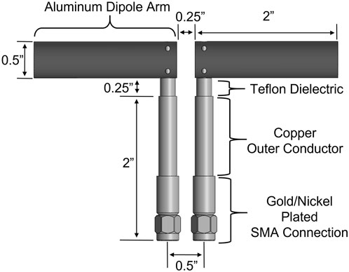
Figure 1. Dipole antenna and RG401 Coax Cable stems.
Each PCB is housed within a Radio Frequency Current-Voltage (RFIV) box. The RFIV boxes are attached to an aluminum ring frame, as shown in Figure 2. The ring is 3/16 inches thick, has an inner diameter of 16 inches, and an outer diameter of 20 inches. This keeps the dipoles aligned, in parallel, and at a fixed distance of 11.2 inches. The additional RFIV boxes placed around the ring, shown in Figure 2, form a circular antenna array, when the dipoles are attached. The array is designed to take multiple mutual-impedance measurements for plasma impedance tomography. The additional dipoles have been removed to avoid unintended capacitive paths between the two measured dipoles.
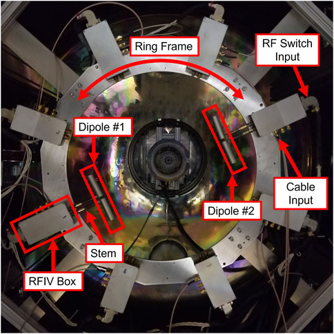
Figure 2. Experimental setup of mutual impedance dipole antenna located in vacuum chamber. Surrounding RFIV boxes and supporting ring fixture are for attaching additional antennas to form the tomography array.
On the RFIV box, shown in Figure 3, there are five external SMA ports, two internal SMA ports, and a rear address/power port. The two external SMA ports, on the end of the RFIV box, attach to the dipole stems. The three SMA ports, on the side of the box, are: voltage in (
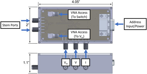
Figure 3. RFIV box and port diagram.
As shown in the circuit board schematic of Figure 4, this switch changes the
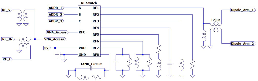
Figure 4. RFIV circuit board diagram. The input signal at RF_IN is routed to the dipole (RF1), one of the six calibration standards (RF2-RF7), or the TANK Circuit (RF8) by the RF Switch.
3 Method
De-embedding (Keysight, 2024) is used to obtain the S-parameters, Equation 1, of the dipoles when they are surrounded by other components. S-parameters are characteristic measurements of a circuits reflection, transmission, or absorption due to an incident voltage wave, as a function of frequency (Caspers, 2010). To aid the de-embedding process, the system is divided by “calibration planes” (cal. plane) into the different components, as shown in Figure 5. A calibration plane is a reference point along a transmission line from which the waves are measured. After measuring the S-parameters between each cal. plane, the de-embedding processes removes each component layer, until only the S-parameters of the dipoles and separating media remain.

Figure 5. Calibration plane layout: Different layers of components to the DUT (plasma): VNA calibration plane (grey), VNA Access ports (green), stem ports (red), and stem-dipole interface (blue).
3.1 Measuring component S-parameters
The de-embedding process requires knowing the S-parameters of the components surrounding the dipoles prior to calibration or to be able to measure them during the calibration. The semi-rigid cable of the stems are modeled as transmission lines, with propagation constants from the published data sheets for RG401 (Pasternack Inc, 2013). By contrast, the far longer cable and circuit S-parameters, extending from the calibrated VNA to the RFIV board, can change due to position or temperature. These cables must be measured in-situ, using the standards built into the RFIV board. Since the balun and cable standards are embedded on the RFIV PCB, these components are less susceptible to temperature variation and movement, and are measured prior to setting up the dipoles. As long as the components on the RFIV board do not change due to environmental conditions (e.g., temperature changes beyond the tolerance of the PCB or electrical discharge), their S-parameters may be assumed constant.
3.1.1 Initial VNA calibration
To acquire all S-parameters, the VNA is first calibrated using a 2-port SOLT calibration (Keysight, 2024) so that there is a known calibration plane from which to measure. The initial VNA calibration includes a through measurement, which the de-embedding builds upon. This eliminates the need for a through measurement between the dipoles. The VNA is calibrated with a BNC Calibration Kit (Maury Microwave Corp. Model No. 8550G). The calibration kit has BNC connections, but SMA connections are used on the RFIV box. So BNC-SMA adapters are attached to SMA cables leading from the VNA. The BNC calibration standards are used to establish the VNA calibration plane at the end of these cables (Additional cables leading from this calibration plane, through the vacuum chamber, and to the RFIV box will be addressed in Section 3.1.3.) The BNC-SMA adapters are removed from the SMA cables and a phase shift is applied to the measured data to move the calibration plane from the BNC connection to the SMA connection. This procedure is described in more detail in Section VI A of the Supplementary Appendix, as it is only an issue when there is a mis-match between the calibration kit and the cable connectors.
3.1.2 Stem S-Parameters
The S-parameters of the dipole stems
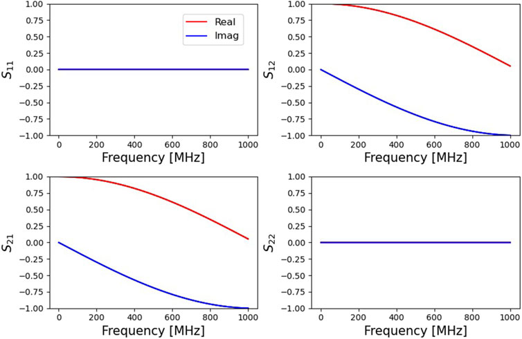
Figure 6. S-parameters of the 2 inch, RG401, stem.
3.1.3 Cable and board S-Parameters
The S-parameters of the cable and PCB path,
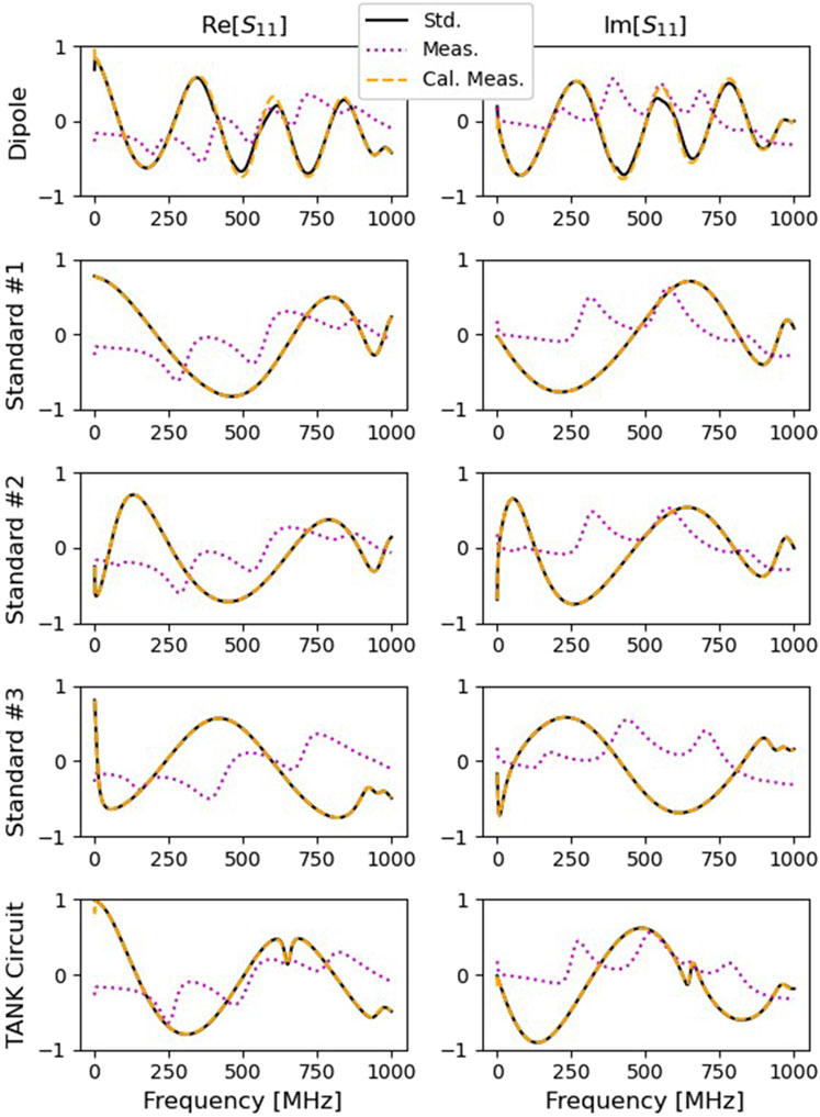
Figure 7. Reflection Coefficients
Since the cable and board are passive, the system is reciprocal:
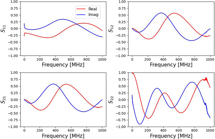
Figure 8. S-parameters of the cable and circuit path between the VNA and the VNA Access on the RFIV board.
3.1.4 Balun S-Parameters
The balun is characterized by a 3-port S-parameter matrix, Equation 6. To measure the 3-port balun with a 2-port VNA, a measurement is made between the two ports while the third port is terminated with a known standard (Poole and Darwazeh, 2015; Satoda and Bodway, 1968). The 2-port S-parameters of the 3-port system are related by Equation 7a, where
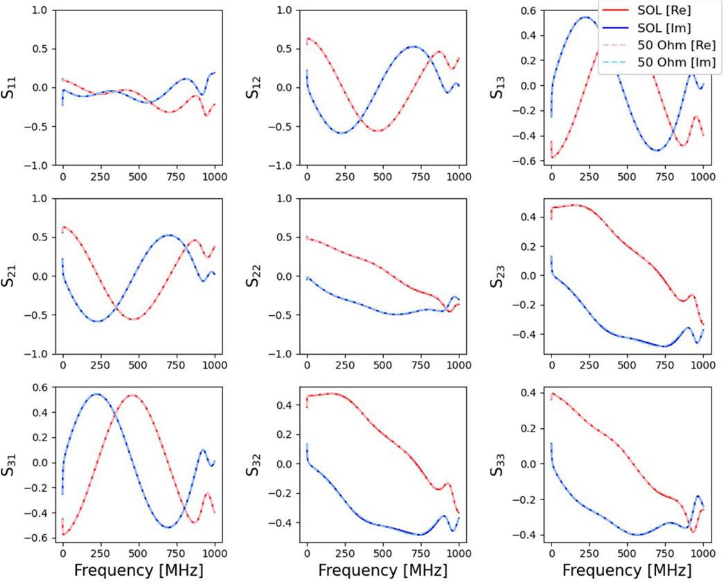
Figure 9. The full 3 × 3 S-parameters of the balun: using the 50
To add more equations and solve all 27 unknowns, three different standards (an open, short, and load) are used, so that there are three different reflection coefficients and nine total measurements. After solving the least-square fit to these 36 equations, the nine balun S-parameters are obtained (the remaining terms being higher order multiples of these terms). The balun S-parameters obtained from this method are also plotted in Figure 9 as solid lines. Compared with the 50
Since the 3-port balun is defined by a 3 × 3 S-parameter matrix, it must be converted to a 2-port 2 × 2 S-parameter matrix, to implement the de-embedding method of Section 3.2. Although a 3-port system can be represented by a 2 × 4 (single line to double line) or 4 × 2 (double line to single line) T-parameter matrix, the inverse of these matrices (such as a Moore–Penrose pseudoinverse) will also be non-square and can only be applied to one-side of a 2 × 4 matrix (Frei et al., 2008). Unfortunately, this does not allow for de-embedding, since the transition from a 4 × 4 matrix to a 2 × 2 matrix looses information.
To solve this problem, the transition from a single-line (2 × 2) to a double-line (4 × 4) balanced system is defined as a transition from a single-line to a mixed system with two modes: “differential” mode and “common” mode (Steer, 2013). The differential mode is what could be considered the expected signal for a dipole, propagating down one of the dipole stems and returning along the other, with the two ports 180° out of phase. In contrast, the common mode propagates down both dipole stems in phase. Since the baluns are designed to reject common modes, the only signal propagating down the stems is assumed to be the differential mode. This is valid above the balun’s 1 MHz lower operating limit. The 3-port S-parameters of the balun are converted to the multi-mode S-parameters
By assuming a negligible common mode, the single line is transitioned directly to the differential mode, at the balun. The S-parameters are reduced to the upper left of Equation 8, resulting in Equation 10 the 2 × 2 S-parameters of the balun
3.2 De-embedding method 1: T-parameter inversion
Once all S-parameters have been acquired, they are converted to T-parameters to perform the necessary linear algebra for de-embedding the dipoles, using Supplementary Equation 11 in Section VI C of the Supplementary Appendix. Although the S-parameters fully characterize the frequency response of the different components, matrix multiplication between S-parameters of sequential components does not cascade their effect (Caspers, 2010). The total S-parameter can not be formed from its parts. To do this operation, the S-parameters must first be converted to T-parameters, which can be cascaded. Multiplication of the T-parameters from all the components, Equation 11, results in
By inverse matrix operation, the inverse T-parameters of the components are manipulated, as shown in Equation 12, to isolate the T-parameters of the “Device Under Test”
3.3 De-embedding method 2: virtual standards
In an attempt to incorporate all of the balun S-parameters, the transition from a single line system to a double line system is modeled in the python S-parameter simulation package scikit-rf (Arsenovic et al., 2022) and calibrated using the SOLT method with virtual standards (Keysight, 2024). Section 3.2 demonstrated a method for de-embedding the dipole system, but this is limited to 2 × 2 matrices and cannot incorporate the balun’s full 3 × 3 S-parameters without reducing it to the differential mode (Salter and Alexander, 1991). In contrast, this section uses the full 3 × 3 S-parameters of the balun, Equation 6, to incorporate both the balun’s common mode and differential mode in the calculations. scikit-rf simulates the different components of the embedded system (stems, balun, and cabling) using their measured S-parameters as inputs. By connecting the nodes of each component and given a known DUT, scikit-rf simulates the entire system presented in Figure 5 and diagrammed in Figure 10a. scikit-rf does the same transfer matrix calculations as Section 3.2, in the background of the program. However, the node connections allow for the user to simply transition from a 2 × 2 matrix to a 3 × 3 matrix, as long as all of the nodes are connected.
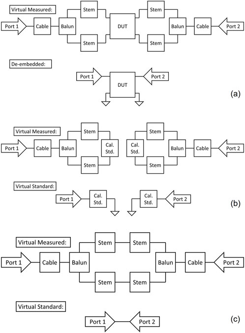
Figure 10. Network diagram of the virtual embedded and de-embedded: (a) DUT, (b) Thru Standards, and (c) Reflection Standards.
A virtual SOLT calibration scheme is applied to this simulation, to move the calibration plane from the VNA, to the dipoles. Ideal virtual S-parameters for a short, open, and load are created as 1-port network elements in the scikit-rf simulation space, while the through is modeled as a direct node-to-node connection. These are then applied as loads at the ends of the simulated cable, balun, and stems to obtain their simulated VNA responses, as diagrammed in Figures 10a, b. The “Virtual Measured” embedded standards are fit to the “Virtual Standards,” using the class skrfSOLT, to obtain a calibration that reduces the measurement to the blue dashed line box in Figure 5. The error terms of this calibration are then applied to future real VNA measurements of the embedded dipoles (using the apply_cal function from the skrfSOLT object) to obtain the de-embedded S-parameters of the dipoles.
The nodal connections between the scikit-rf networks for this procedure are diagrammed in Figure 10. For the reflection standards (short, open, load), the following impedances are used to create their 2 × 2 S-parameter matrices: Matched Load:
3.4 Finite element simulation
To validate the dipole calibration, the measurements are compared with S-parameters calculated from a frequency domain simulation, run in the finite element software: “COMSOL Multiphysics.” (COMSOL AB, 2023) The configuration of the simulation space is shown in Figure 11a. This simulation models: the dipole elements, the stems, the support ring, and the RFIV boxes. Previous work by Brooks et al. (2023), on plasma impedance probes with monopoles, demonstrated a maximum of 20% error between simulations and measurements when the surrounding conductive elements were not taken into consideration. Inclusion of the coaxial stems allows the system to be excited by uniform Coaxial Lumped Ports at the base of the stems. This provides an easily identifiable calibration plane, compared with exciting the system at the dipoles.
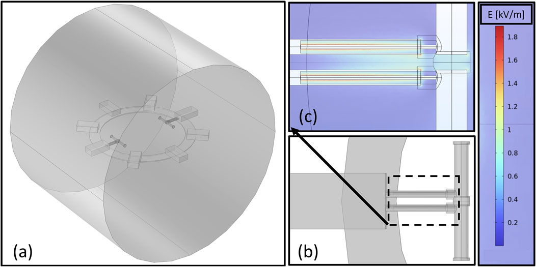
Figure 11. Mutual Impedance Simulation Configuration: (a) Isometric view of simulation space with two dipoles on the ring frame and adjacent RFIV boxes. (b) Top down view of dipole, stem, and RFIV box. (c) Countour plot of the E-field along the stems and between the dipole elements.
The two Coaxial Lumped Ports at the base of a pair of stems excite the differential signal on a single dipole. Due to the two-line nature of the dipoles, the voltages and currents at the ports are exported and converted into S-parameters, rather than exporting the S-parameters directly from the simulation. To excite the system, one dipole has voltage values applied to its ports while the other dipole has a zero-current boundary condition, satisfying the Z-parameter definition (Steer, 2013). To satisfy the 180° phase difference for the differential signal, one of the ports on the active dipole is set to
The voltages
To reduce the required number of mesh nodes and computation time, the metal volume is removed from the simulation and impedance boundary conditions applied to their surfaces. The white space in Figure 11c, shows the contour map of the electric field results and highlights the absence of the metal volumes. Most of the current travels on the surface of a conducting material, but COMSOL also simulates the skin depth for any field that would have entered the volume at higher frequencies. This skin depth is based on the material properties of the given surface. The dielectric behind the Lumped Ports is also removed as it creates a non-realistic path for the fields to travel between the outer and inner conductor, by going around the backside of the port.
The outer surface of the cylindrical simulation volume is a Scattering Boundary, to minimize the reflection of waves back towards the dipoles. The cylinder has a diameter of 1 m and a length of 0.75 m. At this size, increasing the chamber has no effect on the simulation results. The Scattering Boundary works best when the incident waves are normal to the surface, so the cylinder is aligned parallel with the axis of the dipole. At the ends of the cylinder, the flat surface, with a surface normal parallel to the dipoles, has minimal effect, since the transmitted power approaches zero as the wave vector becomes parallel with the dipole (Balanis, 2015).
The main volume of the simulation has a mesh size that ranges from 0.5 mm to 55 mm. Additional mesh refinement was applied to areas with increased field strength. Particularly, the transmission line of the stem and the corner edges of the dipole and stem, shown in Figure 11. These regions have a maximum mesh size of 0.5 mm.
4 Results
First, the de-embedding method is compared to a directly measured known load, validating the method independent of analytical models or simulations. A lossy transmission line cable is used as this known load due to its well defined characteristics. As a sanity check, the de-embedded cable is also compared to the analytical model of a cable, Equation 2.
Second, the mutual impedance of the dipoles are validated by comparing the de-embedded dipole measurement with the finite element simulation, described in Section 3.4. The two different de-embedding methods from Section 3.2 and Section 3.3 are also compared. Although errors exist in all of the validation approaches, reasonable agreement is demonstrated between the measurements, simulation, and analytical model.
4.1 Cable: de-embedded, direct measurement, and analytical model
To embed the cables, two 4 ft long RG316 cables are attached to the baluns as loads for two separate configuration: a transmission configuration and a reflection configuration. For the transmission configuration, each cable is strung between the baluns, connecting the same respective ports of the two RFIV boxes. This means that in Figure 2, the cables are strung diagonally between the RFIV boxes. The network diagram is the same as Figure 10c, but with the stems removed. For the reflection configuration, one cable connects the two ports on each RFIV box. In this case, the cable would take the place of the “Cal. Std.” in Figure 10b, but with the stems removed.
The resulting transmission configuration measurements, in Figure 12, match a single cable, directly measured by the VNA. The RG316 cable is modelled using the published velocity factor and loss data, as described in Section 3.1.2. The resulting reflection configuration measurements show a characteristic cable load, but on the
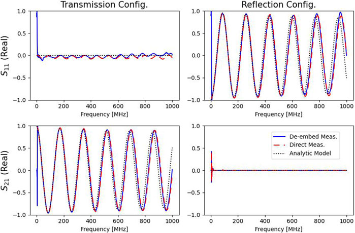
Figure 12. S-parameters of a 4 ft cable in the reflection and transmission configuration: de-embedded by the virtual standard method (blue solid), directly measured with the VNA (red dashed), and analytically modelled (black dotted).
Since the directly measured cables almost exactly match the de-embedded cables, for both the transmission and reflection configurations, these measurements validate the de-embedding process up to the stems’ ports on the RFIV boxes. The analytical cable model closely replicates the directly measured cable, however, there is a phase delay that is equivalent to adding an extra 2 cm electrical length to the 4 ft long cable. There is also a ripple in the
4.2 Dipole: measurements, calibration methods, and simulation
The dipoles de-embedded in air are compared with the finite element simulations and presented in Figure 13. The reflection coefficients
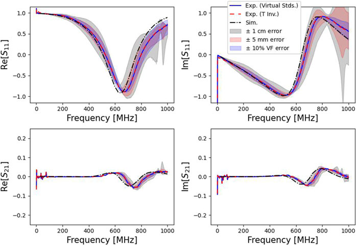
Figure 13. S-parameters of simulated and de-embedded dipoles, using both de-embedding methods. Includes shaded regions identifying the spread of the sensitivity analyses.
The plasma density is determined from the plasma resonance, so this shift in frequency, rather than any resulting error in magnitude, is the primary concern for the mutual impedance probes. The plasma density
By assuming an electrical length delay of 1.0 cm for the measurement, the maximum difference between the S-parameter magnitudes is halved. This electrical delay would represent an unaccounted for additional cable length in the system. However, the drawback to assuming this electrical length delay is that, below 400 MHz, the average difference between the simulation and de-embedded
A sensitivity analysis was performed on the calibrated system’s final results. The artificial error was introduced as a phase shift in the VNA’s calibration plane for each measurement in the de-embedding process. The sensitivity study looked at the final results of the de-embedded dipoles, if the VNA calibration plane was off by ±1 cm or ±5 mm. The phase shifts were applied to each measurement involved in the process: the full system measurement, the true measurement of the RFIV standards, the measurement of the RFIV standards at the end of the cables, the true measurement of balun standards, and the through measurement of the balun with standards attached at the third port. Every combination of error (e.g., +1 cm, 0 cm, and -1 cm) at each measurement step was calculated and the spread of the possible range is plotted in Figure 13 as the grey (
From this analysis, it is clear that with a large enough variation in the calibration plane, the difference between the simulated and experimental data could be accounted for. Although the variation in the stem velocity factor can also account for similar changes, more than a 10% variation is needed to account for the difference seen in this data. Although the data sheet (Pasternack Inc., 2013) does not provide confidence values for the data, a
The two de-embedding methods are both applied to the measured data, for comparison in Figure 13. Both methods have almost the exact same result, but there is a deviation in
Finally, the calibrated S-parameters are converted to Z-parameters using Supplementary Equation 13 and plotted in Figure 14. The
To find the plasma density, the model for self-impedance from Balmain (Balmain, 1964) is fit to the self-impedance, or an adapted version of the Balmain model is fitted to the mutual impedance. More complex analytical solutions to the mutual-impedance measurement have also previously been implimented (Storey et al., 1969; Pottelette et al., 1975; Chasseriaux et al., 1972; Debrie et al., 1976). From these equations, the plasma resonance is a function of the plasma density, magnetic field, distance between the dipoles, collision frequency, sheath thickness, and the angle between the dipole and the magnetic field. The derivation of the mutual impedance model and sample plasma measurements goes beyond the scope of this work, which is focused on calibrating the dipole instrument.
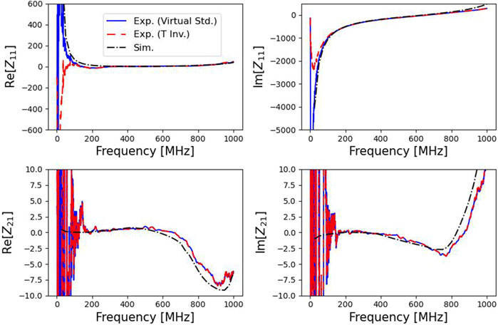
Figure 14. Z-parameters of simulated and de-embedded dipoles, using both de-embedding methods.
5 Discussion
The calibration method is validated by the previous plots, despite slight errors between simulated and measured data. The major validating piece of evidence, is the agreement between the de-embedded and directly measured cables. Despite potential error in the VNA calibration, the de-embedding method returns the same result as the direct measurement.
5.1 Sources of error
For this calibration procedure, four sources of error were identified that can be mitigated:
1) The common mode error below 100 MHz, in the conventional T-parameter inversion method, is corrected by incorporating the full balun S-parameters in the Virtual Standards method. By using the balun three-port model, in the Virtual Standards method, information from the balun’s common mode is conserved. The common mode is otherwise discarded when the balun is represented as a two-port model, in the T-parameter inversion method, with the balun’s single line as one port and the differential mode as the second port. Although the balun’s reported operational frequency extends down to 1 MHz, the common mode clearly begins to become noticeable at higher frequencies. By simply implementing the Virtual Standards method, this low frequency error is removed.
2) The low frequency noise in
3) The BNC connections were found to cause a variable calibration. BNC connections are not a fixed fit, but allow play for the cables to turn. Due to small capacitive differences in the contact surfaces, when turned, the impedance changes with movement. This can form a ripple in the calibrated magnitude. Since SMAs are screwed on and form a static contact, they were substituted for all the BNC connections, successfully removing the ripple effect in the calibrated VNA magnitude.
4) The differences between the measured and modelled data suggest that there is still an issue with the VNA calibration. The analytical cable model, in Figure 12 has a delay from the directly measured cable. Also, the
6 Conclusion
This work has presented an in-situ calibration method for de-embedding two dipoles located in a vacuum chamber. The intended application has been for mutual impedance plasma density measurements and plasma impedance tomography measurements. The in-situ calibration standards account for cable heating and cable travel, two significant factors in plasma experiments that may require continued recalibration, while the instruments are inaccessible in the vacuum chamber. Two de-embedding methods were presented: 1) the Virtual Standards method and 2) the T-parameter inversion method. Both agree with one-another almost exactly except below 100 MHz, where the Virtual Standards have better agreement with the dipole simulation. It is assumed that the Virtual Standards account for the common mode in the balun, which becomes more prominent near the balun’s lower frequency limit of 1 MHz.
The de-embedding method was validated by comparing it with a direct measurement of a 4 ft length of cable. There was very little discrepancy between the directly measured cables and the de-embedded cables. Comparison of the directly measured cables, de-embedded cables, and ideal transmission line model, showed a phase shift equivalent to an electrical length of 2 cm, between the ideal and measured values. The dipole de-embedding was compared with COMSOL simulations, which also had a phase delay, but only for an electrical delay of 1 cm. This error equates to a 6% lower plasma density measurement. The measurements and models suggest that the phase shift error is associated with the VNA calibration standards, while the calibration method is still valid. Other sources of error included: the variable capacitance of the BNC connections and the VNA’s signal power, which can both be mitigated.
This calibration method gives the ability to remotely calibrate an array of dipoles without performing any through measurements. The presented method has several advantages over other dipole calibration methods: 1) Plasma measurements (including magnetized plasma) can be performed without uncertainty related to temperature and bending effects on the connecting cables, which lead to errors at higher frequencies. 2) Balun common mode errors at low frequencies are significantly reduced. 3) Calibration effort and time is greatly reduced for a multiprobe tomographic setup. Future work will consist of: First, demonstrating mutual impedance plasma measurements at frequencies in the 10s–100 s of MHz range, now capable with this calibration method. Second, perform a 2D plasma tomographic measurement and inversion with the 8-probe array, shown in Figure 2.
Data availability statement
The raw data supporting the conclusions of this article will be made available by the authors, without undue reservation.
Author contributions
MP: Writing–original draft, Writing–review and editing. ET: Writing–review and editing. GG: Writing–review and editing.
Funding
The author(s) declare that financial support was received for the research and/or publication of this article. This work was supported by the U.S. Naval Research Laboratory (NRL) base funding and M.C. Paliwoda was specifically funded by the 2023-2024 Karle Fellowship.
Conflict of interest
The authors declare that the research was conducted in the absence of any commercial or financial relationships that could be construed as a potential conflict of interest.
Generative AI statement
The author(s) declare that no Generative AI was used in the creation of this manuscript.
Publisher’s note
All claims expressed in this article are solely those of the authors and do not necessarily represent those of their affiliated organizations, or those of the publisher, the editors and the reviewers. Any product that may be evaluated in this article, or claim that may be made by its manufacturer, is not guaranteed or endorsed by the publisher.
Supplementary material
The Supplementary Material for this article can be found online at: https://www.frontiersin.org/articles/10.3389/fspas.2025.1519446/full#supplementary-material
References
Adler, A., and Holder, D. (2021). Electrical impedance tomography: methods, history and applications. 2nd ed. (Boca Raton, FL, USA: CRC Press).
C63.5 (2017). American national standard for electromagnetic compatibility–radiated emission measurements in electromagnetic interference (EMI) control–calibration and qualification of antennas (9 kHz to 40 GHz). New York, NY, USA: IEEE.
Anritsu(2012). “Understanding VNA Calibration,”, Richardson, TX, USA: Anritsu Company. Available online at: https://anlage.umd.edu/Anritsu_understanding-vna-calibration.pdf (Accessed March 26, 2025).
Arsenovic, A., Hillairet, J., Anderson, J., Forstén, H., Rieß, V., Eller, M., et al. (2022). Scikit-rf: an open source Python package for Microwave network creation, analysis, and calibration [Speaker’s Corner]. IEEE Microw. Mag. 23 (1), 98–105. doi:10.1109/mmm.2021.3117139
Bahnsen, A., Jespersen, M., Ungstrup, E., Pottelette, R., Malingre, M., Decreau, P. M. E., et al. (1988). First VIKING Results: High Frequency Waves. Phys. Scr. 37 (3), 469–474. doi:10.1088/0031-8949/37/3/032
Balmain, K. (1964). The Impedance of a Short Dipole Antenna in a Magnetoplasma. IEEE Trans. Antennas Propag. 12 (5), 605–617. doi:10.1109/tap.1964.1138278
Barr, J. T., and Pervere, M. J. (1989). A Generalized Vector Network Analyzer Calibration Technique. In: 34th ARFTG conference digest. Ft. Lauderdale, USA: IEEE; 51–60.
Beghin, C., Karczewski, J. F., Poirier, B., Debrie, R., and Massevitch, N. (1982). The ARCAD-3 ISOPROBE Experiment for High Time Resolution Thermal Plasma Measurements. Ann. Geophys. 38 (5), 615–629. Available online at: https://www.researchgate.net/publication/256453819 (Accessed March 26, 2025).
Bockelman, D. E., and Eisenstadt, W. R. (1995). Combined Differential and Common-Mode Scattering Parameters: Theory and Simulation. IEEE Trans. Microw. Theory Tech. 43 (7), 1530–1539. doi:10.1109/22.392911
Brooks, J. W., Tejero, E. M., Paliwoda, M. C., and McDonald, M. S. (2023). High-speed Plasma Measurements with a Plasma Impedance Probe. Rev. Sci. Instrum. 94 (8), 083506. doi:10.1063/5.0157625
Bucciantini, L., Henri, P., Wattieaux, G., Califano, F., Vallières, X., and Randriamboarison, O. (2022). In situ Space Plasma Diagnostics With Finite Amplitude Active Electric Experiments: Non-Linear Plasma Effects and Instrumental Performance of Mutual Impedance Experiments. J. Geophys. Res. Space Phys. 127 (12), e2022JA030813. doi:10.1029/2022ja030813
Bucciantini, L., Henri, P., Dazzi, P., Wattieaux, G., Lavorenti, F., Vallières, X., et al. (2023a). Instrumentation for Ionized Space Environments: New High Time Resolution Instrumental Modes of Mutual Impedance Experiments. J. Geophys. Res. Space Phys. 128 (2), e2022JA031055. doi:10.1029/2022ja031055
Bucciantini, L., Henri, P., Wattieaux, G., Lavorenti, F., Dazzi, P., and Vallières, X. (2023b). Space Plasma Diagnostics and Spacecraft Charging. The Impact of Plasma Inhomogeneities on Mutual Impedance Experiments. J. Geophys. Res. Space Phys. 128 (8), e2023JA031534. doi:10.1029/2023ja031534
Burger, S., Taute, W., and Hoeft, M. (2018). “Accurate Permittivity Measurement of PTFE,” in Australian Microwave symposium (AMS) (Brisbane, Australia: IEEE), 33–34.
Carlisle (2017). Understanding Phase Versus Temperature Behavior. Carlisle Interconnect Technologies; Rev 030817. Available online at: https://www.amphenol-cit.com/wp-content/pdfs/application-notes/Phase_vs_Temp_Behavior_CIT.pdf (Accessed March 26, 2025).
Caspers, F. (2010). RF engineering basic concepts: S-parameters. Geneva, Switzerland: CERN. Available online at: https://cds.cern.ch/record/1415639/files/p67.pdf (Accessed March 26, 2025).
Cathers, S., LoVetri, J., Jeffrey, I., and Gilmore, C. (2023). Electromagnetic Imaging System Calibration With 2-Port Error Models. IEEE Open J. Antennas Propag. 4, 1142–1153. doi:10.1109/ojap.2023.3329356
Chasseriaux, J. M., Debrie, R., and Renard, C. (1972). Electron Density and Temperature Measurements in the Lower Ionosphere as Deduced from the Warm Plasma Theory of the h.f. Quadrupole Probe. J. Plasma Phys. 8 (2), 231–253. doi:10.1017/s0022377800007108
COMSOL AB (2023). “COMSOL Mutliphysics v. 6.1,”. Stockholm, Sweden. Available online at: www.comsol.com (Accessed March 26, 2025).
Debrie, R., Arnal, Y., and Illiano, J. M. (1976). Measurement of low electronic temperatures in unmagnetized plasmas. Phys. Lett. A 56 (2), 95–96. doi:10.1016/0375-9601(76)90155-9
Decreau, P. M. E., Beghin, C., and Parrot, M. (1978a). Electron Density and Temperature, as Measured by the Mutual Impedance Experiment on Board GEOS-1. Space Sci. Rev. 22, 581–595. doi:10.1007/bf00223942
Decreau, P. M. E., Etcheto, J., Knott, K., Pedersen, A., Wrenn, G. L., and Young, D. T. (1978b). Multi-Experiment Determination of Plasma Density and Temperature. Space Sci. Rev. 22, 633–645. doi:10.1007/bf00223945
Keysight (2004). De-embedding and embedding S-parameter networks using a vector network analyzer. Santa Rosa, CA, United States: Agilent Technologies; Available online at: https://www.keysight.com/us/en/assets/7018-06806/application-notes/5980-2784.pdf (Accessed March 26, 2025).
Dittmann, K., Küllig, C., and Meichsner, J. (2012). 160 GHz Gaussian Beam Microwave Interferometry in Low-Density Rf Plasmas. Plasma Sources Sci. Technol. 21 (2), 024001. doi:10.1088/0963-0252/21/2/024001
Ehrlich, P. (1953). Dielectric Properties of Teflon from Room Temperature to 314-Degrees-C and from Frequencies of 10_2 to 10_5 c/s. J. Res. Natl. Bureau Stand. 51 (4), 185. doi:10.6028/jres.051.024
Engen, G. F., and Hoer, C. A. (1979). Thru-Reflect-Line: An Improved Technique for Calibrating the Dual Six-Port Automatic Network Analyzer. IEEE Trans. Microw. Theory Tech. 27 (12), 987–993. doi:10.1109/tmtt.1979.1129778
Ferrero, A., and Pisani, U. (1992). Two-Port Network Analyzer Calibration Using an Unknown ‘Thru. IEEE Microw. Guid. Wave Lett. 2 (12), 505–507. doi:10.1109/75.173410
Frei, J., Cai, X. D., and Muller, S. (2008). Multiport S-Parameter and T-Parameter Conversion With Symmetry Extension. IEEE Trans. Microw. Theory Tech. 56 (11), 2493–2504. doi:10.1109/TMTT.2008.2005873
Gilet, N., Henri, P., Wattieaux, G., Myllys, M., Randriamboarison, O., Béghin, C., et al. (2019). Mutual Impedance Probe in Collisionless Unmagnetized Plasmas With Suprathermal Electrons—Application to BepiColombo. Front. Astronomy Space Sci. 6, 16. doi:10.3389/fspas.2019.00016
Gilmore, C., Mojabi, P., Zakaria, A., Ostadrahimi, M., Kaye, C., Noghanian, S., et al. (2010). A Wideband Microwave Tomography System With a Novel Frequency Selection Procedure. IEEE Trans. Biomed. Eng. 57 (4), 894–904. doi:10.1109/tbme.2009.2036372
Grard, R. (1997). Influence of Suprathermal Electrons upon the Transfer Impedance of a Quadrupolar Probe in a Plasma. Radio Sci. 32 (3), 1091–1100. doi:10.1029/97rs00254
Greenberg, K. E., and Hebner, G. A. (1993). Electron and Metastable Densities in Parallel-Plate Radio-Frequency Discharges. J. Appl. Phys. 73 (12), 8126–8133. doi:10.1063/1.353451
Haynes, M., Stang, J., and Moghaddam, M. (2012). Microwave Breast Imaging System Prototype with Integrated Numerical Characterization. Int. J. Biomed. Imaging 2012 (706365), 1–18. doi:10.1155/2012/706365
Hebner, G. A., Verdeyen, J. T., and Kushner, M. J. (1988). An Experimental Study of a Parallel-Plate Radio-Frequency Discharge: Measurements of the Radiation Temperature and Electron Density. J. Appl. Phys. 63 (7), 2226–2236. doi:10.1063/1.341060
Hirose, M., and Komiyama, K. (2007). “Novel Method for Antenna Measurements Using SOL Without T Calibration,” in Antennas and propagation society international symposium (Honolulu, HI, USA: IEEE), 605–608.
Hirose, M., and Komiyama, K. (2010). “A Novel Full 2-Port Calibration Method for Antenna Measurements Using Sol Standards without through Procedure,” in Conference on precision electromagnetic measurements (Daejeon, South Korea: IEEE), 329–330.
IEEE standard methods for measuring electromagnetic field strength of sinusoidal continuous waves, 30 Hz to 30 GHz. (1991). New York, NY, USA: IEEE.
Issakov, V., Sene, B., Aguilar, E., Werthof, A., Jenei, S., and Weigel, R. (2017). “Considerations on Accurate Characterization of Differential Devices Using Baluns,” in 47th European Microwave conference (Nuremberg, Germany: IEEE), 660–663.
Iwasaki, T., and Tomizawa, K. (2003). “Measurement of S-parameters of Balun and Its Application to Determination of Complex Antenna Factor,”, 1. Istanbul, Turkey: IEEE, 62–65. doi:10.1109/icsmc2.2003.1428193IEEE international symposium on electromagnetic compatibility
Johansson, F. L., Eriksson, A. I., Vigren, E., Bucciantini, L., Henri, P., Nilsson, H., et al. (2021). Plasma Densities, Flow, and Solar EUV Flux at Comet 67P: A Cross-Calibration Approach. Astronomy and Astrophysics 653, A128. doi:10.1051/0004-6361/202039959
Knight, D. A., Nothofer, A., and Alexander, M. J. (2004). Comparison of calibration methods for monopole antennas, with some analysis of the capacitance substitution method. Teddington, Middlesex, UK: National Physical Laboratory. Available online at: https://eprintspublications.npl.co.uk/3108/ (Accessed March 26, 2025).
Konstroffer, L. (1999). Finding the Reflection Coefficient of a Differential One-Port Device. RF Semiconductor. Available online at: http://www.rfsilicon.com/home/measurement/19990102.pdf (Accessed March 26, 2025).
Kovtun, Y. V., Siusko, Y. V., Skibenko, E. I., and Skibenko, A. I. (2018). Experimental Study of Inhomogeneous Reflex-Discharge Plasma Using Microwave Refraction Interferometry. Ukrainian J. Phys. 63 (12), 1057. doi:10.15407/ujpe63.12.1057
Krämer, M., Clarenbach, B., and Kaiser, W. (2006). A 1 Mm Interferometer for Time and Space Resolved Electron Density Measurements on Pulsed Plasmas. Plasma Sources Sci. Technol. 15 (3), 332–337. doi:10.1088/0963-0252/15/3/006
Krupka, J., Derzakowski, K., Riddle, B., and Baker-Jarvis, J. (1998). A Dielectric Resonator for Measurements of Complex Permittivity of Low Loss Dielectric Materials as a Function of Temperature. Meas. Sci. Technol. 9 (10), 1751–1756. doi:10.1088/0957-0233/9/10/015
Kruppa, W., and Sodomsky, K. F. (1971). An Explicit Solution for the Scattering Parameters of a Linear Two-Port Measured with an Imperfect Test Set (Correspondence). IEEE Trans. Microw. Theory Tech. 19 (1), 122–123. doi:10.1109/tmtt.1971.1127466
Lukas, C., Müller, M., Schulz-von Der Gathen, V., and Döbele, H. F. (1999). Spatially Resolved Electron Density Distribution in an RF Excited Parallel Plate Plasma Reactor by 1 Mm Microwave Interferometry. Plasma Sources Sci. Technol. 8 (1), 94–99. doi:10.1088/0963-0252/8/1/012
McLean, J. S. (2008). Rigorous Representation of a Shielded Three-Port Balun in the Simulation of an Antenna System. IEEE Trans. Electromagn. Compat. 50 (3), 762–765. doi:10.1109/temc.2008.927921
Mini-Circuits, (2018). More than just a phase: understanding phase stability in RF test cables. Mini-Circuits; Available online at: https://www.minicircuits.com/app/AN46-004.pdf.
Nagora, U., Sinha, A., Pathak, S. K., Ivanov, P., Tanna, R. L., Jadeja, K. A., et al. (2020). Design and Development of 140 GHz D-band Phase Locked Heterodyne Interferometer System for Real-Time Density Measurement. J. Instrum. 15 (11), P11011–1. doi:10.1088/1748-0221/15/11/P11011
Nemez, K., Baran, A., Asefi, M., and LoVetri, J. (2017). Modeling Error and Calibration Techniques for a Faceted Metallic Chamber for Magnetic Field Microwave Imaging. IEEE Trans. Microw. Theory Tech. 65 (11), 4347–4356. doi:10.1109/tmtt.2017.2694823
Newell, A., Baird, R., and Wacker, P. (1973). Accurate Measurement of Antenna Gain and Polarization at Reduced Distances by an Extrapolation Technique. IEEE Trans. Antennas Propag. 21 (4), 418–431. doi:10.1109/tap.1973.1140519
Niemöller, N., Schulz-von Der Gathen, V., Stampa, A., and Döbele, H. F. (1997). A Quasi-Optical 1 Mm Microwave Heterodyne Interferometer for Plasma Diagnostics Using a Frequency-Tripled Gunn Oscillator. Plasma Sources Sci. Technol. 6 (4), 478–483. doi:10.1088/0963-0252/6/4/004
Ostadrahimi, M., Mojabi, P., Gilmore, C., Zakaria, A., Noghanian, S., Pistorius, S., et al. (2011). Analysis of Incident Field Modeling and Incident/Scattered Field Calibration Techniques in Microwave Tomography. IEEE Antennas Wirel. Propag. Lett. 10, 900–903. doi:10.1109/lawp.2011.2166849
Overzet, L. J. (1995). Microwave Diagnostic Results From the Gaseous Electronics Conference Rf Reference Cell. J. Res. Natl. Inst. Stand. Technol. 100 (4), 401. doi:10.6028/jres.100.030
Pasternack Inc, (2013). RG401 coax cable with copper. Irvine, CA, USA: Pasternack Inc.; Available online at: https://www.pasternack.com/images/ProductPDF/RG401-U.pdf.
Poole, C., and Darwazeh, I. (2015). Microwave active circuit analysis and design. 1st ed. London, UK: Academic Press.
Pottelette, R., Rooy, B., and Fiala, V. (1975). Theory of the Mutual Impedance of Two Small Dipoles in a Warm Isotropic Plasma. J. Plasma Phys. 14 (2), 209–243. doi:10.1017/s0022377800009533
Riddle, B., Baker-Jarvis, J., and Krupka, J. (2003). Complex Permittivity Measurements of Common Plastics over Variable Temperatures. IEEE Trans. Microw. Theory Tech. 51 (3), 727–733. doi:10.1109/tmtt.2003.808730
Rumiantsev, A., and Ridler, N. (2008). VNA Calibration. IEEE Microw. Mag. 9 (3), 86–99. doi:10.1109/mmm.2008.919925
Salter, M. J., and Alexander, M. J. (1991). EMC Antenna Calibration and the Design of an Open-Field Site. Meas. Sci. Technol. 2 (6), 510–519. doi:10.1088/0957-0233/2/6/004
Satoda, Y., and Bodway, G. E. (1968). Three-Port Scattering Parameters for Microwave Transistor Measurement. IEEE J. Solid-State Circuits 3 (3), 250–255. doi:10.1109/jssc.1968.1049894
Smith, A. A. (1982). Standard-Site Method for Determining Antenna Factors. IEEE Trans. Electromagn. Compat. EMC-24 (3), 316–322. doi:10.1109/temc.1982.304042
Steer, M. (2013). Microwave and RF design: a systems approach. 2nd ed. Edison, NJ, USA: SciTech Publishing.
Storey, L. R. O., Aubry, M. P., Meyer, P., and Thomas, J. O. (1969). “Quadripole Probe for Study of Ionospheric Plasma Resonances,”, 1. New York, NY, USA: American Elsevier Publishing Co., Inc., 303–332. Available online at: https://www.researchgate.net/publication/234338521 (Accessed March 26, 2025)
Storey, L. R. O. (1998a). “Mutual-Impedance Techniques for Space Plasma Measurements,” in Measurement techniques in space plasma: fields. No. 103 in geophysical monograph series. Editors F. Pfaff, E. Borovsky, and T. Young (Washington, D. C., USA: American Geophysical Union), 155–160. Available online at: https://www.researchgate.net/publication/252301917 (Accessed March 26, 2025).
Storey, L. R. O., and Cairo, L. (1998b). “Measurement of Plasma Resistivity at ELF,” in Measurement techniques in space plasma: fields. No. 103 in geophysical monograph series. Editors R. F. Pfaff, J. E. Borovsky, and D. T. Young (Washington, D. C., USA: American Geophysical Union), 211–216.
Storey, L. R. O. (2013). “What’s Wrong with Space Plasma Metrology?,” in Geophysical monograph series. Editors R. F. Pfaff, J. E. Borovsky, and D. T. Young (Washington, D. C., USA: American Geophysical Union), 17–22.
Trotignon, J. G., Beghin, C., Lagoutte, D., Michau, J. L., Matsumoto, H., Kojima, H., et al. (2006). Active Measurement of the Thermal Electron Density and Temperature on the Mercury Magnetospheric Orbiter of the BepiColombo Mission. Adv. Space Res. 38, 686–692. doi:10.1016/j.asr.2006.03.031
Trotignon, J. G., Michau, J. L., Lagoutte, D., Chabassiere, M., Chalumeau, G., Colin, F., et al. (2007). RPC-MIP: The mutual impedance probe of the ROSETTA plasma consortium. Space Sci. Rev. 128, 713–728. doi:10.1007/s11214-006-9005-1
Wattieaux, G., Henri, P., Gilet, N., Vallières, X., and Deca, J. (2020). Plasma Characterization at Comet 67P between 2 and 4 AU from the Sun with the RPC-MIP Instrument. Astronomy and Astrophysics 638, A124. doi:10.1051/0004-6361/202037571
Keywords: plasma tomography, mutual impedance probe, de-embedding method, plasma impedance probe, dipole calibration
Citation: Paliwoda MC, Tejero EM and Gatling GR (2025) De-embedding a pair of dipoles to calibrate the mutual impedance plasma density diagnostic. Front. Astron. Space Sci. 12:1519446. doi: 10.3389/fspas.2025.1519446
Received: 29 October 2024; Accepted: 18 March 2025;
Published: 09 April 2025.
Edited by:
Julio Urbina, The Pennsylvania State University (PSU), United StatesCopyright © 2025 Paliwoda, Tejero and Gatling. This is an open-access article distributed under the terms of the Creative Commons Attribution License (CC BY). The use, distribution or reproduction in other forums is permitted, provided the original author(s) and the copyright owner(s) are credited and that the original publication in this journal is cited, in accordance with accepted academic practice. No use, distribution or reproduction is permitted which does not comply with these terms.
*Correspondence: M. C. Paliwoda, cGFsaXdvZGFtYXR0aGV3QGdtYWlsLmNvbQ==