 Yukuan Chang
 Fang Yuan1
- 1State Key Laboratory on Integrated Optoelectronics, Institute of Semiconductors, Chinese Academy of Sciences, Beijing, China
- 2School of Materials Science and Optoelectronic Technology, University of Chinese Academy of Sciences, Beijing, China
Light detection and ranging (LiDAR) is the most important active remote sensing tool and is widely used in civilian and military fields. There are a number of methods to drive laser diodes; the most common circuit topologies are capacitor-discharge resonant circuits. However, the performance of the silicon (Si)-based switching device limits the development of Light detection and ranging, such as the large figure of merit (FOM) and the stray inductance. Although different methods have been reported to resolve these problems, there are still great challenges in reducing the pressure on Light detection and ranging driver design. Hence, this work presents a gallium nitride (GaN)–Si hybrid integrated driver for a Light detection and ranging system. In the circuit, the switching power device uses GaN instead of a Si-based device, because GaN enables much better performance for pulsed-laser operation due to its near-ideal switching performance. Furthermore, a GaN push–pull driver stage between the GaN power device and the Si-based driver integrated circuit (IC) was innovatively introduced, which is integrated in the same chip with the GaN power device, thereby effectively reducing the parasitic parameters of the signal chain and enhancing the system reliability. The design and implementation of the Si-based IC and GaN IC are based on 0.18 µm 80–120 V Bipolar-CMOS-DMOS (BCD) technology and 0.5 µm p-GaN technology, respectively. The experimental results suggest that the proposed driver circuit output pulse width is 12.6 ns, and it can normally operate at 10 MHz with turn-on/turn-off delay is 11.94 ns. In addition, the driver was capable of generating approximately 8.25 A current pulses through a low ohmic load with a pulse width of approximately 12.4 ns. This work plays a vital role in promoting the development of information equipment and aerospace equipment such as precise ranging, high-efficiency power supplies, and high-speed motors.
1 Introduction
LiDAR, a radar system that detects the target position, speed, and other characteristics by emitting a laser beam, is widely used in military, automotive, medical, and other fields [1–7]. A typical LiDAR system consists of a laser transmitter, an optical receiver, and an information-processing system. The laser transmitter converts the electrical pulses into optical pulses and emits them, and the optical receiver detects the optical pulses reflected from the target and restores them to electrical pulses, so that the distance between the emission source and the detected object can be calculated [8, 9]. This technique is also known as time of flight (TOF) detection.
Laser transmitters used in LiDAR systems are usually near-infrared semiconductor lasers, edge-emitting lasers, or vertical-cavity surface-emitting lasers [10]. These laser diodes behave similarly to rectifiers in terms of device electrical characteristics, that is, when forward biased beyond a certain threshold current, the device emits laser radiation with an output optical power roughly proportional to the forward current. Therefore, a pulsed-laser beam of corresponding intensity can be obtained by driving the laser with a certain intensity of current pulses. The pulse width and pulse amplitude of the laser determine the two most important technical parameters of the TOF LiDAR: ranging resolution and detection distance. A shorter pulse width gives better resolution while a higher pulse peak current increases the detection distance [11, 12].
The laser of a LiDAR is driven by a dedicated circuit, which supplies a large amount of current for a short period of time. The most common circuit topology to implement such a driver is a capacitor-discharge resonant circuit [13], as shown in Figure 1, where the power switch M1 must be able to withstand high voltages, conduct peak currents, and respond in nanoseconds or less. However, the traditional Si-based switching device has become the limiting factor in the development of LiDAR systems for two reasons: first, the large gate charge due to the large power switch size needed to meet the current and voltage requirements greatly slows the turn-on of the metal–oxide–semiconductor field-effect transistor (MOSFET) [14]. Second, MOSFETs are vertical devices with connections on both sides of the die, so it is forced to use an external package form, which adds substantial inductance in both the power loop and the gate drive loop [15].
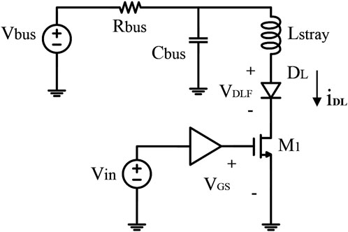
FIGURE 1. Conventional implementation of a capacitor-discharge resonant driver.
Recently, gallium nitride (GaN) power devices have attracted a lot of attention because of the heterojunction two-dimensional electron gas (2DEG) channel structure. These devices have several overwhelming advantages over silicon (Si)-based devices, such as higher operating frequency, lower on-resistance, and higher blocking capacity [16–18]. By comparing Si MOSFETs and GaN power devices at the same current rating, GaN power devices have a smaller figure of merit (FOM; = Qg × Ron. Qg is the gate charge of the power device, Ron is on-resistance of the power device) and package inductance [19], which is especially suitable for high-frequency, high-integration, and energy-efficient LiDAR applications.
Some examples of laser drivers based on GaN power devices have been reported. Glaser [20] proposed a performance-optimized pulsed-laser diode driver based on a GaN FET. Ma et al. [21] proposed a digital-type GaN driver with a laser-diode peak-current-correction (LDPCC) loop and a current–pulse balancer (CPB) loop for LiDAR systems, which is a driver prototype that uses GaN high-electron-mobility transistors (HEMTs) as power switches, while the predriver and auxiliary circuits use silicon transistors. Although a series of considerable research results has been achieved in optimizing drive circuit performance, there are still certain challenges in reducing the pressure on LiDAR driver design, specifically for reducing the parasitic inductance between driver output stage and the GaN power switch. Due to the existence of parasitic inductance, the gate voltage ringing during the whole pulse-generation cycle may cause it to exceed the safe-operating region, putting GaN power device reliability at risk [22].
This work presents a GaN–Si hybrid integrated driver based on the existing research. The circuit is a heterogeneous mixture of GaN integrated circuit (IC) and high-performance Si-based IC, which innovatively introduces a GaN push–pull driver stage between the GaN power devices and the Si-based driver IC. Through system-level optimization, this work minimizes the influence of the parasitic parameters, thereby stabilizing the power switch device turn on and enabling narrower output pulse widths and higher drive rates. This design has obvious advantages in narrow-pulse-width LiDAR applications that require extremely high performance with respect to output pulse width, drive rate, and stability. The experimental results suggest that the proposed driver circuit output pulse width is 12.6 ns, and the driver can normally operate at 10 MHz with turn-on/turn-off delay is 11.94 ns. The driver was capable of generates approximately 8.25 A current pulses through a low ohmic load with a pulse width of approximately 12.4 ns.
2 Materials and methods
2.1 Concept of the proposed architecture
As shown in Figure 2, an integrated driver of a heterogeneous mixture of GaN IC and high-performance Si-based IC is proposed, where the main parasitic capacitance, inductance, and resistance are also illustrated. The parasitic inductance L and parasitic resistance R represent the bonded-wire components on the printed circuit board (PCB) circuit; C1 is the equivalent parasitic capacitance of the Si-based IC output node and C2 is the equivalent parasitic capacitance of the GaN IC input node.
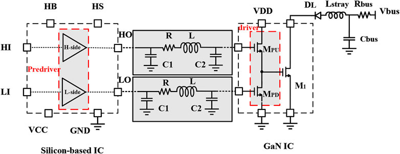
FIGURE 2. Proposed driver composed of a heterogeneous mixture of gallium nitride (GaN) integrated circuit (IC) and high-performance silicon (Si) -based IC.
The circuit includes two parts: the Si-based IC and the GaN IC. The Si-based IC is a high-stability and high-integration half-bridge predriver with high-side and low-side output channels, driving a GaN push–pull output driver stage MPU and MPD, respectively. VCC and GND is the power and ground of the low side, The voltage range of the low-side drive is 0V–5V. HB and HS is the power and floating ground of the high side. HB is generated off chip, we using Bootstrap circuit to generate high side power supply voltage HB. The voltage range of high-side driver is VDD to VDD + VCC. Specific circuits will be described thoroughly in Section 2.2.2. The GaN IC is composed of the driver stage and the power switch. They are integrated in the same chip to minimize the interconnection parasitic, and reduce the time constraint for charging the gate capacitance of the power switch device M1. The enhanced GaN MPU and MPD form a push–pull output driver stage for M1. MPU and MPD are much smaller than M1, therefore the interconnection node between the Si and the GaN chip can be a position with lower parasitic capacitance in the signal transmission link, which can reduce the gate voltage ringing under the same parasitic inductance in the gate drive loop.
2.2 Circuit realization
2.2.1 GaN IC with push–pull driver stage
This work proposes a GaN IC with a push–pull driver stage and power switch on the same chip, as shown in Figure 3. Previous approaches have been reported for GaN ICs using p-type (p-GaN) -gate HEMTs [23]. However, complementary p-channel HEMTs are still not viable due to poor hole mobility in the GaN material [24]. Hence, the presented GaN IC driver stage is designed with two n-type enhanced GaN. To better appreciate the effectiveness of this solution, the Si-based IC uses a half-bridge structure to drive the enhanced GaN MPU and MPD. Because the half-bridge Si-based IC uses two signals with opposite phases that are non-overlapping, when the signals turn MPD off, MPU will turn on, and the M1 gate node is pulled up. Similarly, when the signals turn MPD on, MPU will turn off, and the M1 gate node is pulled down. The GaN IC is designed in 0.5 μm p-GaN technology, which uses a Si-based substrate, and the structure of the GaN FET is a p-type gate structure.
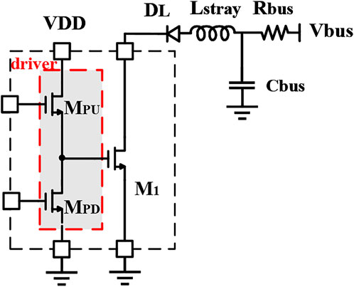
FIGURE 3. Circuit diagram of the GaN IC with push–pull driver stage.
2.2.2 Predriver
The topology of the predriver configuration is shown in Figure 4. The circuit is an integrated half-bridge predriver, which has high stability and high integration. It includes a Schmitt trigger circuit, dead-time control circuit, pulse generator circuit, level shifter circuit, pulse filter circuit, reset–set (RS) flip-flop circuit, and low-side predriver circuit.
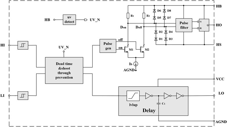
FIGURE 4. Circuit realization of the predriver structure.
2.2.2.1 Schmitt trigger
The role of the Schmitt trigger circuit is to reduce the interference of the input signal. As can be seen from Figure 4, input signals HI and LI are processed by Schmidt circuit, and the output signals HO and LO correspond to the input HI and LI through the logic levels. Because the Schmitt trigger has a hysteresis function, the entire logic circuit gives an anti-interference ability to the input signal.
2.2.2.2 Dead time control
The dead time setting prevents the high-side and the low-side power switches from being turned on at the same time, to avoid burning out. The dead time control circuit is divided into two parts: a dead-time generation circuit and a dead-time setting circuit. Figure 5 shows a block diagram of a dead-time generation circuit. The inverters with tail current sources I1 and I2 and the capacitor C1 form a delay circuit to obtain a delay signal that inverts the rising edge of the high- and low-side signals. The inverted signal of the original input signal and the generated delay signal take part in the NOR operation to obtain the high- and low-side gate-switching signals with dead time. The UV_N signal is an under-voltage protection signal. When the high-voltage power supply HB has an under-voltage occurrence, the UV_N signal output is high, so that both the high- and low-side signals become 0 after passing through the dead-time control circuit.
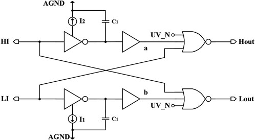
FIGURE 5. Schematic of the dead-time control circuit.
The tail currents of the two branches on the high and low sides of the circuit are equal, that is, I1 = I2, so that when the high- and low-side power tubes are turned on, the dead time is equal. The expression for the dead time is as follows:
where I1 is the tail current of the inverter, Vth is the flipping threshold of the buffer and VCC is the low-side power supply in Section 2.1.
2.2.2.3 Pulse generator
The pulse generator produces two pulses to drive the level shifter circuit formed by two high-voltage double-diffused MOSs (DMOSs). The generation of the two pulses reflects the rising and falling edges of the HI signal, respectively. Figure 6 shows the structure of the pulse generator circuit.
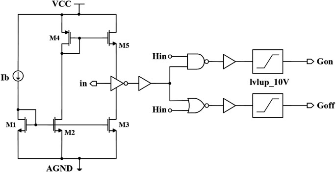
FIGURE 6. Schematic of the pulse generator circuit.
The principle of the pulse generator is to use a constant current to charge/discharge the capacitor, thereby controlling the width of the generated pulse signal. The pulse signal passes through the level conversion circuit and translates the voltage domain of the logic levels from low voltage to high voltage.
2.2.2.4 Level shifter circuit
The pulse signals Gon and Goff generated by the pulse generator are used to drive the level shifter circuit formed by two high-voltage DMOSs. When Gon and Goff turn on M1 and M2, the resistors R1 and R2 will generate a pulse Don or Doff, which is low level relative to the floating level HS. After these two signals pass through the pulse filter, the RS flip-flop working on the floating level is set or reset. Figure 7 is a schematic diagram of the level shift circuit.
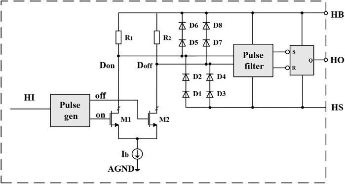
FIGURE 7. Schematic of level shifter circuit.
When the DMOS M1 or M2 is turned on, the pull-down voltage on R1 and R2 can be expressed as:
2.2.2.5 Pulse filter circuit and RS flip-flop circuit
After the pulses Don and Doff that are generated by the level shifter circuit pass through the pulse filter, the RS flip-flop on the floating level is set or reset. This series of actions resynthesizes the rising and falling edges of the HI signal into a complete pulse width signal, which is the entire process of converting the HI signal input at the logic reference level into the output drive signal HO at the floating level. Because each DMOS is only turned on for a short period of time when the RS flip-flop is set or reset, the power loss is much smaller than that of two DMOSs that are continually turned on, especially when the switching frequency of the system is very low. Figure 8 is a block diagram of a pulse filter circuit and an RS flip-flop circuit. Both the pulse filter circuit and the RS flip-flop circuit use HB and HS as the power supply and ground, and HS is the floating ground of the high side.
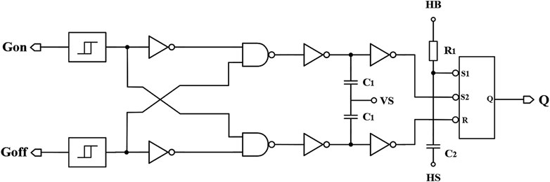
FIGURE 8. Schematic of the pulse filter and RS flip-flop circuit.
The introduction of R1 and C2 is to set the RS flip-flop during the power-on process. The high-side circuit realizes the conversion of the HI signal input at the logic reference level into the output drive signal HO of the floating level.
2.2.2.6 Low-side circuit
The low-side circuit converts the input low-level signal LI (5 V/0 V) into a driving signal (5 V/0 V) with driving ability, the delay block is to obtain the same delay as the high-side path.
Because there is no high-voltage power consumption and the problem of conversion such as suspension level, therefore, the low-side circuit can be greatly simplified. However, because the signal HI passes through the pulse generator, the level shifter circuit, the pulse filter, and the RS trigger circuit during the transmission of the high-side path, a delay module is required on the low-side path. The introduced delay module produces the same delay as that on the high-side path, so that after the HI and LI signals pass through the high-side path and the low-side path, respectively, the obtained delays are consistent. Figure 9 is a schematic diagram of the low-side predriver circuit.
FIGURE 9. Schematic of the low-side predriver circuit.
3 Results
The implementations of the Si-based IC and GaN IC are based on 0.18 µm 80–120 V BCD technology and 0.5 μm p-GaN technology, respectively. Figure 10 shows the micrograph and testbench photos using the proposed structure. The layout of the PCB minimized the total inductance [25]. Moreover, a high-speed testing strategy is also used in this design, including a Kelvin connection for gate/drain and impedance matching with the sub-miniature A (SMA) connector at the gate/drain electrodes as well.
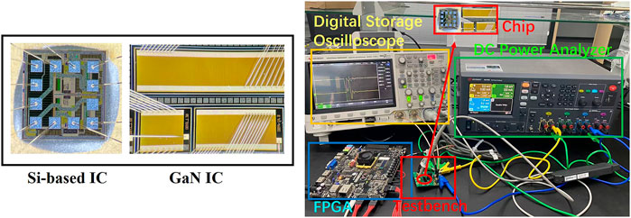
FIGURE 10. Chip micrograph (left) and Testbench of the proposed driver circuit (right).
3.1 Simulation results
Figure 11 shows the diagram of the simulation model equivalent circuit. The parasitic inductance L = 2 nH; the value of 2 nH is based on the estimated package inductance of the laser and the stray inductance due to the PCB. The parasitic resistance R = 100 mΩ; the parasitic capacitance and gate input capacitance are equivalent to Ctotal, which is 175 pF.
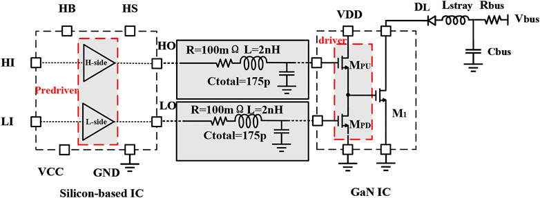
FIGURE 11. Diagram of the simulation model equivalent circuit.
The design of the entire circuit was simulated and optimized using Advanced Design System (ADS) [17]. The parasitic inductances are estimated from the circuit layout. The simulated waveform results are shown in Figure 12. The conventional capacitor-discharge resonant driver simulation result is shown in Figure 12A; the equivalent capacitance between the driver stage and the power switch is 700 pF, which is the parasitic capacitance and gate input capacitance of power switch M1 due to the size of the device. As we can see from the simulation result, the ringing of the gate voltage VM1_g = 6.5 V, which is very dangerous for a GaN device, thereby affecting the stability of the system. Keeping the same circuit board inductance and resistance as for the conventional circuit, the proposed circuit simulation results are shown in Figures 12B,C. It is clear that with the proposed circuit, the gate voltage ringing is significantly reduced, to 4.8 V. Because the size of MPD and MPU are much smaller than M1, the equivalent capacitance between the driver stage and the power switch is 175 pF and the gate voltage ringing occurs at 5.487 V and 5.272 V, respectively, which are acceptable and significantly mitigated the harm to M1. Therefore, the proposed circuit is a better choice for LiDAR applications.
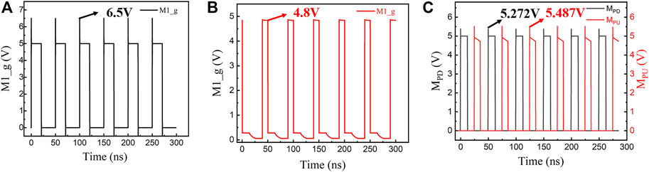
FIGURE 12. Simulation results comparing the proposed structure and conventional capacitor-discharge resonant driver circuit waveforms: (A) conventional capacitor-discharge resonant driver waveform of the M1 gate; (B) the proposed driver waveform of the M1 gate; (C) the proposed driver waveform of the MPD gate (black) and MPU gate (red).
3.2 Test results
Based on the simulation discussion in Section 3.1, the test comparison between the proposed circuit and the conventional circuit is shown in Figure 13. The test results of the proposed circuit are shown in Figure 13A; the input pulse signal generated by the field programmable gate array (FPGA) is 100 ns, the driver output width is 12.6 ns. Under the same test conditions for the input pulse signal, the conventional driver output width is 26.6 ns, as shown in Figure 13B.
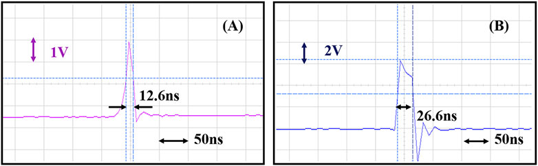
FIGURE 13. Experimental waveforms of the proposed driver and the conventional driver: (A) proposed driver output result; (B) conventional driver output result.
The proposed circuit has much smaller output width than the conventional circuit, which is consistent with the simulation results. However, there is still a slight deviation between the actual measurement results and the simulation results due to the power device conduction loss and switching loss.
The current drive capability was measured with a small resistor load; by measuring the drain voltage of the power switch M1, the current can be obtained. In this case the peak value of the current pulse can be written as follows:
Where Vbus is the supply voltage, Rbus is the resistor load, and VM1_d is the drain voltage of the power switch M1. Under the test conditions of Vbus = 15 V and Rbus = 1 Ω, the drain voltage of M1 can be observed from Figure 14, which is 6.75 V when the pulse width is 12.4 ns. Based on Eq. 3–1, the peak current can be calculated as 8.25 A.
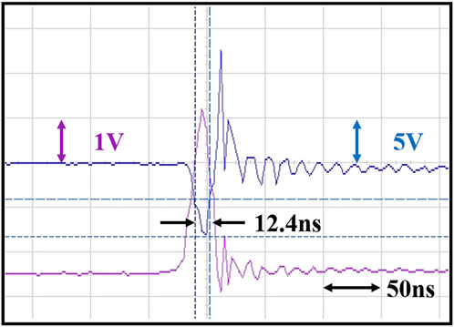
FIGURE 14. Experimental waveforms of the power switch M1 gate and drain voltage.
The propagation delay of the proposed high-side and low-side drivers at 10 MHz are shown in Figure 15. VCC is set to 5 V and VDD is 10 V, VCC is the low-side power supply and VDD is the power supply of push-pull driver stage in Section 2.1. It can be observed from Figures 15A, B that the turn-on propagation delay of the high side is 11.94 ns, and the turn-off propagation delay is 11.7 ns. Figures 15C, D show the turn-on propagation delay of the low side is 8.44 ns, and the turn-off propagation delay is 18.6 ns. It is worth noting that the signal generated by the FPGA will be divided into two signals and preprocessed by an inverter to make sure the low side and high side signals will not be high at the same time, so the turn-off propagation delay includes the dead time of the inverter, which is 10 ns.
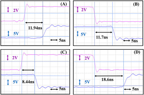
FIGURE 15. Propagation delay of the proposed driver at 10 MHz: (A) turn-on delay of the high-side driver; (B) turn-off delay of the high-side driver; (C) turn-on delay of the low-side driver; (D) turn-off delay of the low-side driver.
These experimental results indicate that with the proposed GaN–Si hybrid integrated driver, the power device ringing and spikes are significantly reduced, and the proposed structure has excellent performance in high switching frequency operation, and the propagation delay at 10 MHz is 11.94 ns. The driver generates approximately 8.25 A current pulses through a low ohmic load with a pulse width of approximately 12.4 ns. At this point, the pulse width of the input signal generated by the FPGA is 100 ns, and the output pulse width is 12.6 ns. When the pulse width of the input signal is adjusted to be narrower, this structure can be used to obtain a narrower pulse width output.
4 Discussion
The design of a GaN–Si hybrid integrated driver for narrow-pulse and high-current LiDAR applications is presented. The experimental results suggest that the proposed driver circuit output pulse width is 12.65 ns, and the circuit can normally operate at 10 MHz with turn-on/turn-off delay is 11.94 ns. Additionally, the driver generates approximately 8.25 A current pulses with a pulse width of approximately 12.4 ns. By comparison with the conventional capacitor-discharge resonant driver structure, the ringing and spikes of the power device are significantly reduced, showing its future potential in a wide range of scenarios. The circuit driver is especially suitable to meet LiDAR applications for high resolution and increased detection range. However, to minimize the pulse width and to maximize the peak current the total parasitic inductance of the current loop should be minimized. This can be achieved by carefully designing the PCB and minimizing the length of the bonding wires.
Because this is still a non-monolithic driver, there are still inductances that cannot be avoided. During the switch turn-on cycle, the large time derivative of the currents through L cause a voltage drop on the power switch gate. The lower the gate voltage, the lower the maximum current that the power switch can handle when operating in the linear region, with low drain-source voltage VDS. This may require compensating for the reduced current handling capability with an increase of the switch gate width or settling for a lower peak current specification. Therefore, future research on this work will be focused on an all-GaN driver solution, to further reduce the impact of parasitic inductance.
Data availability statement
The original contributions presented in the study are included in the article/supplementary material, further inquiries can be directed to the corresponding author.
Author contributions
Conceptualization, YK and FY; methodology, YK and FY; software, YK and YC; validation, YK, FY, and XZ; formal analysis, YK and YC; investigation, YK; resources, XZ.; data curation, YK; supervision, FY and XZ; writing—original draft preparation, YK; writing—review and editing, YK and FY; project administration, FY and XZ; funding acquisition, XZ All authors have read and agreed to the published version of the manuscript.
Acknowledgments
YC would like to thank Jiacheng Jiang, and Fuye Han at Advanced Semiconductors of Intelligences and Technologies, Haining, China for helping with the chip test.
Conflict of interest
The authors declare that the research was conducted in the absence of any commercial or financial relationships that could be construed as a potential conflict of interest.
Publisher’s note
All claims expressed in this article are solely those of the authors and do not necessarily represent those of their affiliated organizations, or those of the publisher, the editors and the reviewers. Any product that may be evaluated in this article, or claim that may be made by its manufacturer, is not guaranteed or endorsed by the publisher.
References
1. Zimmermann M, Gestwa M, Koenig C, Wolfram J, Klasen S, Lederle A. First results of LiDAR-aided helicopter approaches during NATO DVE-mitigation trials. CEAS Aeronaut J (2019) 10:859–74. doi:10.1007/s13272-018-0354-8
2. Kechagias-Stamatis O, Aouf N, Richardson MA. 3D automatic target recognition for future LiDAR missiles. IEEE Trans Aerosp Electron Syst (2016) 52:2662–75. doi:10.1109/TAES.2016.150300
3. Lin TC, Tan DS, Tang HL, Chien SC, Chang FC, Chen YY, et al. Pedestrian detection from LiDAR data via cooperative deep and hand-crafted features. In: 25th IEEE International Conference on Image Processing (ICIP); 7-10 October 2018; Athens, Greece (2018). p. 1922–6. doi:10.1109/ICIP.2018.8451578
4. Liero A, Klehr A, Hoffmann T, Prziwarka T, Heinrich W. GaN laser driver switching 30 A in the sub-nanosecond range. In: European Microwave Conference; London, 3–4 Oct. 2016 (2016). p. 1389–92. doi:10.1109/EuMC.2016.7824612
5. Wolfram B, Oliver B, Cyrill S. Map-based precision vehicle localization in urban environments. In: Robotics: Science and systems III. United States: MIT Press (2008). p. 121–8.
6. Furstenberg K, Ahlers F. Development of a low-cost automotive laser scanner - the EC project MiniFaros. In: M Gereon, editor. Advanced microsystems for automotive applications (AMAA). Berlin, Heidelberg: Springer Berlin Heidelberg press (2011). p. 149–58. doi:10.1007/978-3-642-21381-6_15
7. Li Y, Ibanez-Guzman JJISPM. Lidar for Autonomous Driving: The principles, challenges, and trends for automotive lidar and perception systems. IEEE Signal Process Mag (2020) 37(4):50–61. doi:10.1109/MSP.2020.2973615
8. Glaser J. How GaN power transistors drive high-performance lidar: Generating ultrafast pulsed power with GaN FETs. IEEE Power Electron Mag (2017) 4(1):25–35. doi:10.1109/MPEL.2016.2643099
9. Wenzel H, Klehr A, Liero A, Christopher H, Fricke J, Knigge A, et al. High pulse power wavelength stabilized 905 nm laser bars for automotive LiDAR. In: 2019 IEEE High Power Diode Lasers and Systems Conference (HPD); Coventry, United Kingdom, 9-10 Oct. 2019 (2019). p. 7–8. doi:10.1109/HPD48113.2019.8938682
10. Liu JY, Sun Q, Fan Z, Jia Y, TOF lidar development in autonomous vehicle. In: 2018 IEEE 3rd Optoelectronics Global Conference (OGC); 4-7 September 2018; Shenzhen, China (2018). p. 185–90. doi:10.1109/OGC.2018.8529992
11. Nissinen J, Kostamovaara J. A high repetition rate CMOS driver for high-energy sub-ns laser pulse generation in SPAD-based time-of-flight range finding. IEEE Sensors J (2016) 16(6):1628–33. doi:10.1109/JSEN.2015.2503774
12. Tajfar A, Zamprogno M, Villa F, Zappa F A 20 A sub-nanosecond integrated cmos laser diode driver for high repetition rate SPAD-based direct time-of-flight measurements. In: 2018 International Conference on Computing, Electronics & Communications Engineering (iCCECE); 16-17 August 2018; Southend, United Kingdom (2018). p. 272–6. doi:10.1109/iCCECOME.2018.8658623
13. Glaser J. High power nanosecond pulse laser driver using an GaN FET. In: PCIM Europe 2018; International Exhibition and Conference for Power Electronics, Intelligent Motion, Renewable Energy and Energy Management; 5 - 7 Jun 2018; Nuremberg, Germany (2018).
14. Erickson RW, Maksimovic D. Fundamentals of power electronics. 2nd ed. Berlin, Heidelberg: Springer Berlin Heidelberg press (2001). p. 1103p.
15. Glaser J (2021) eGaN FETs for lidar - getting the most out of the EPC9126 laser driver. Available at: https://epc-co.com/epc/Portals/0/epc/documents/application-notes/AN027%20Getting-the-Most-out-of-eGaN-FETs.pdf [Accessed July 17, 2022].
16. Chen KJ, Häberlen O, Lidow A, Tsai C, Ueda T, Uemoto Y, et al. GaN-on-Si power technology: Devices and applications. IEEE Trans Electron Devices (2017) 64(3):779–95. doi:10.1109/TED.2017.2657579
17. Liero A, Klehr A, Schwertfeger S, Hoffmann T, Heinrich W. Laser driver switching 20 A with 2 ns pulse width using GaN. In: 2010 IEEE MTT-S International Microwave Symposium; 23-28 May 2010; Anaheim, California, USA (2010). p. 1110–3. doi:10.1109/MWSYM.2010.5517952
18. Reusch D, Strydom J, Lidow A. (2015). A new family of GaN transistors for highly efficient high frequency DC-DC converters. 2015 IEEE Applied Power Electronics Conference and Exposition (APEC). 15-19 March 2015, Charlotte, North Carolina, USA: doi:10.1109/APEC.2015.7104619
19. Ming X, Ye ZK, Lin ZY, Qin Y, Zhou Q, Zhang B. A fully-integrated GaN driver for time-of-flight lidar applications. In: 34th IEEE International Symposium on Power Semiconductor Devices and ICs (ISPSD); 22-25 May 2022; Vancouver (2022). p. 169–72. doi:10.1109/ISPSD49238.2022.9813668
20. Glaser J. Optimizing performance of a pulsed laser diode driver based on a GaN FET. In: 2019 IEEE Workshop on Wide Bandgap Power Devices and Applications in Asia (WiPDA Asia); 23-25 May 2019; Taipei, Taiwan (2019). doi:10.1109/WiPDAAsia.2019.8760309
21. Ma YS, Lin ZY, Lin YT, Lee CY, Huang TP, Chen KH, et al. 29.6 A digital-type GaN driver with current-pulse-balancer technique achieving sub-nanosecond current pulse width for high-resolution and dynamic effective range LiDAR system. In: 2019 IEEE International Solid- State Circuits Conference (ISSCC); 17-21 February 2019; San Francisco, California, USA (2019). p. 466–8. doi:10.1109/ISSCC.2019.8662308
22. Meneghini M, Hilt O, Wuerfl J, Meneghesso G. Technology and reliability of normally-off GaN HEMTs with p-type gate. Energies (2017) 10(2):153. doi:10.3390/en10020153
23. Wei J, Tang G, Xie R, Chen KJ. GaN power IC technology on p-GaN gate HEMT platform. Jpn J Appl Phys (2019) 59(SG):SG0801. doi:10.7567/1347-4065/ab5b63
24. Zheng Z, Zhang L, Song W, Feng S, Xu H, Sun J, et al. Gallium nitride-based complementary logic integrated circuits. Nat Electron (2021) 4(8):595–603. doi:10.1038/s41928-021-00611-y
Keywords: lidar, TOF, GaN, laser driver, narrow-pulse
Citation: Chang Y, Yuan F, Kou Y and Zhang X (2022) A GaN–Si hybrid integrated driver for narrow-pulse and high-current LiDAR applications. Front. Phys. 10:1063730. doi: 10.3389/fphy.2022.1063730
Received: 07 October 2022; Accepted: 06 December 2022;
Published: 20 December 2022.
Edited by:
Chen Xu, Beijing University of Technology, ChinaReviewed by:
Luhong Mao, Tianjin University, ChinaValentino Liberali, University of Milan, Italy
Yibo Dong, University of Shanghai for Science and Technology, China
Copyright © 2022 Chang, Yuan, Kou and Zhang. This is an open-access article distributed under the terms of the Creative Commons Attribution License (CC BY). The use, distribution or reproduction in other forums is permitted, provided the original author(s) and the copyright owner(s) are credited and that the original publication in this journal is cited, in accordance with accepted academic practice. No use, distribution or reproduction is permitted which does not comply with these terms.
*Correspondence: Xu Zhang, zhangxu@semi.ac.cn