 Yuzhu Pan1
 Xin Wang1*Yubing Xu1Yuwei Li1
 Elias Emeka Elemike2
 Ahmed Shuja3Qing Li1Xiaobing Zhang1Jing Chen1Zhiwei Zhao1Wei Lei1*
- 1School of Electronic Science and Engineering, Joint International Research Laboratory of Information Display and Visualization, Southeast University, Nanjing, China
- 2Chemistry Department of North West University, Mafikeng, South Africa
- 3Centre for Advanced Electronics and Photovoltaic Engineering, International Islamic University, Islamabad, Pakistan
Introducing hole/electron transporting and blocking layers is considered to enhance the performance of electronic devices based on organic–inorganic hybrid halide perovskite single crystals (PSCs). In many photodiodes, the hole/electron transporting or blocking materials are spin-coated or thermal-evaporated on PSC to fabricate heterojunctions. However, the heterojunction interfaces due to lattice mismatch between hole/electron, transporting or blocking materials and perovskites easily form traps and cracks, which cause noise and leakage current. Besides, these low-mobility transporting layers increase the difficulty of transporting carriers generated by photons to the electrode; hence, they also increase the response time for photo detection. In the present study, MAPbCl3-MAPbBr2.5Cl0.5 heterojunction interfaces were realized by liquid-phase epitaxy, in which MAPbBr2.5Cl0.5 PSC acts as an active layer and MAPbCl3 PSC acts as a hole blocking layer (HBL). Our PIN photodiodes with epitaxial MAPbCl3 PSC as HBL show better performance in dark current, light responsivity, stability, and response time than the photodiodes with spin-coated organic PCBM as HBL. These results suggest that the heterojunction interface formed between two bulk PSCs with different halide compositions by epitaxy growth is very useful for effectively blocking the injected charges under high external electric field, which could improve the collection of photo-generated carriers and hereby enhance the detection performance of the photodiode. Furthermore, the PIN photodiodes made of PSC with epitaxial HBL show the sensitivities of 7.08 mC Gyair−1 cm−2, 4.04 mC Gyair−1 cm−2, and 2.38 mC Gyair−1 cm−2 for 40-keV, 60-keV, and 80-keV X-ray, respectively.
Graphical Abstract. Stratiform MAPbBr2.5Cl0.5/MAPbCl3 heterojunction perovskite single crystal is fabricated by epitaxy growth and then poly-TPD is spin-coated on the face of MAPbBr2.5Cl0.5 to form an electron blocking layer. Interestingly, the PIN perovskite photodiode-based epitaxial hole blocking layers reveal higher photoelectric properties and satisfactory detectability for 40- to 80-keV X-ray.
Introduction
Perovskite is a promising candidate among new-generation opto-electronic material for applications in solar cells and light-emitting diodes owing to its outstanding optical and electrical characteristics (Kojima et al., 2009; Tan et al., 2014; Ju et al., 2018). In particular, organic–inorganic hybrid halide lead single crystal perovskites (MAPbX3, where MA = CH3NH3 and X = Cl, Br, or I) with high atomic numbers have been studied. Excellent carrier mobility, low trap density, long carrier diffusion length, and high absorption coefficient indicate that they could be applied not only in regular ultraviolet, visible, and near-infrared light, but also in X-ray and gamma-ray detection and imaging (Wang et al., 2015; Yakunin et al., 2015; Wei et al., 2016; Gill et al., 2018). For perovskite photodiodes, the vertical (sandwich-like) topology structures generated by introducing hole/electron transporting or blocking layers are considered to enhance the performance (Wang and Kim, 2017; Zeng et al., 2017). In many devices based on perovskite crystal, n-type materials including fullerene-derivative phenyl-C61-butyric acid methyl ester (PCBM), ZnO, and TiO2 act both as electron transport layers (ETL) and hole blocking layers (HBL). The p-type polymers including poly[N,N′-bis(4-butylphenyl)-N,N′-bis(phenyl)-benzidine] (poly-TPD), poly(ethylenedioxythiophene):polystyrene sulfonate (PEDOT:PSS), poly(9-vinlycarbazole) (PVK), and poly[bis(4-phenyl)(2,4,6-trimethylphenyl)amine] (PTAA) are used both as hole transport layers (HTLs) and electron blocking layers (EBLs) (Dai et al., 2014; Jara et al., 2014; Liu and Kelly, 2014; Malinkiewicz et al., 2014).
The intimate contact between the active layer and hole/electron blocking layers is essential for blocking injected charges and effectively collecting carriers to the electrodes (Chen et al., 2017; Cheng et al., 2019). However, these additional layered transporting and blocking layers deposited by spin-coating or thermal evaporation have a low mobility lifetime and high trap density because these layers are amorphous and have lattice mismatch on PSC interfaces (Lin et al., 2015; Zhang et al., 2017). In addition, surface traps or cracks are easily formed when they deposit large-area and 10-nm-thick functional layers that would cause large noise and leaking current (Fang and Huang, 2015; Wang et al., 2019). MAPbBr2.5Cl0.5 PSC has been proven to possess large resistivity, high mobility, and low degree of lattice mismatch as compared to MAPbCl3 PSC (Sutherland and Sargent, 2016; Jiang et al., 2019; Ou et al., 2019). Therefore, it is feasible to fabricate lattice-matched heterojunctions with the energy band gradient between MAPbBr2.5Cl0.5 PSC and MAPbCl3 PSC by epitaxy growth. This would significantly decrease the leaking current and accelerate carrier transport, leading to a high-performance PSC photodetector (Li et al., 2019b).
This article demonstrates a facile process for fabricating stratiform MAPbBr2.5Cl0.5/MAPbCl3 heterojunction PSCs by liquid-phase epitaxial growth. MAPbBr2.5Cl0.5 PSC mainly acts as an active layer to absorb photons and n-type MAPbCl3 PSC as HBL to decrease the positive charges injected from the anode. Subsequently, p-type organic molecules poly-TPD are deposited on the opposite faces of doped MAPbBr2.5Cl0.5 PSC to form HTL to block the negative charges injected from the cathode. Finally, the gold and silver films are deposited on the faces of poly-TPD and MAPbCl3 PSC as anode and cathode, respectively. The device with electron transport material PCBM and C60 as HBL was fabricated by spin coating to compare with our device. Our PIN photodiode supplanted organic micro molecule with MAPbCl3 PSC acting as HBL on MAPbBr2.5Cl0.5 PSC shows a lower dark current density, greater responsivity, and faster response time. It demonstrates the superiority of taking lattice matched heterojunction by epitaxy growth in the fabricating of perovskite diode. Furthermore, the PIN photodiode with epitaxial MAPbCl3 PSC as HBL also shows excellent performance on low-energy X-ray detection due to it being a few millimeters in thickness.
Materials and Methods
Materials
Methylamine ethanol solution (CH3NH2, 33 wt.%), hydrobromic acid (HBr, 48 wt.%), hydrochloric acid (HCl, 37 wt.%), poly-TPD, PCBM, and C60 (99.99%) were obtained from Aladdin. N,N-Dimethylformamide (DMF) and dimethyl sulfoxide (DMSO) were obtained from Alfa Aesar. Lead chloride (PbCl2, 99.9%) and lead bromide (PbBr2, 99.9%) were purchased from Sigma-Aldrich. All commercial products were used as received.
PSC Growth
To synthesize MACl and MABr, 1 mol L−1 HCl and 1 mol L−1 HBr were poured into 1 mol L−1 methylamine ethanol solution. Powder-like MACl and MABr were obtained after drying in vacuum at 150°C. To prepare the precursor solutions of MAPbCl3, 4.05 g (1 mol L−1) of MACl, 16.72 g (1 mol L−1) of PbCl2, and 45 ml of DMSO were dissolved in 60 ml of DMF. To prepare the precursor solutions of MAPbBr2.5Cl0.5, 6.72 g (1 mol L−1) MABr, 16.52 g (0.75 mol L−1) of PbBr2, and 4.17 g (0.25 mol L−1) of PbCl2 were dissolved in 60 ml of DMF. The solutions were filtered by a polytetrafluoroethylene (PTFE) filter with a 30-μm pore size. The filtrate was then transferred to a culture dish and placed on a programmable heating station (IKA-RET control-visc). For MAPbCl3 PSC, the temperature was first set at 45°C and raised by 0.2°C h−1 until it reached 60°C. For epitaxial and pristine MAPbBr2.5Cl0.5 PSC, the temperature was first set at 50°C and raised by 0.2°C h−1 until it reached 65°C.
Device Fabrication
To fabricate epitaxial EBL photodiodes, 100-nm poly-TPD and 50-nm Au electrodes were deposited on the face of epitaxial MAPbBr2.5Cl0.5 PSCs, and 50-nm Ag electrodes were deposited on the face of MAPbCl3 PSCs by thermal evaporation in vacuum. For the spin-coated EBL device, 100-nm poly-TPD and a 50-nm Au electrode were deposited on one face of pristine MAPbBr2.5Cl0.5 PSC by thermal evaporation in vacuum and 10-nm C60 and 50-nm PCBM were deposited on the opposite face by spin coating at 1,000 r min−1 in 15 s. Subsequently, Ag electrodes were deposited on it by thermal evaporation in vacuum. To optimize the epitaxial PIN photodiode surface, a diamond wire with a diameter of 0.08 mm was used to remove the extra surrounding at a sawing speed of 3,000 r min−1.
Measurements
XRD patterns were obtained by X'TRA (Switzerland). SEM images and EDX were obtained by Quanta 200 FEI (USA). PL (photoluminescence) patterns were obtained by Edinburgh instruments FS5 (UK). Dark current density–voltage (J–V) characteristics were measured by a Keithley 4,200 semiconductor analyzer in darkness. The response time and transmit time were measured using an Agilent oscilloscope with a Keithley 2,400 as the voltage source and a 365-nm pulsed Nd:YAG laser with 6-ns pulse width at 20 Hz as the illumination source. Responsivity spectra were measured using Zolix tunable 500-W xenon arc lamp light as the illumination source and a Keithley 4,200 semiconductor analyzer. The photocurrent in X-ray detection performance was measured by a Keithley 6,487 Pico ammeter, and the X-ray dose rate was obtained by a commercial dosimeter (FJ-347A, China). The X-ray source was provided by Nanjing Perlove Medical Equipment Company.
Results and Discussion
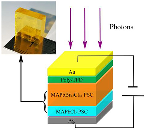
Pristine MAPbCl3 PSCs considered as n-type semiconductors were grown by various temperature crystallization methods. The precursor solution was heated from 45 to 60°C for 80 h to grow MAPbCl3 PSCs (Wang et al., 2017). First, one unit in bulk of MAPbCl3 PSCs was synthesized by low-cost solution processes, as shown in Figure 1A. Then, it was placed into the precursor solution of MAPbBr2.5Cl0.5 to induce liquid-phase epitaxial growth, in which the solution was heated from 50 to 65°C for 100 h. The MAPbBr2.5Cl0.5 PSC slowly grew on the top and side of MAPbCl3 in the precursor solution. Finally, the heterojunction PSC could be extracted from the solution with MAPbBr2.5Cl0.5 enfolding MAPbCl3 PSC as shown in Figure 1B. In order to fabricate the PIN photodiode, p-type poly-TPD thin film was deposited on the surface of the MAPbBr2.5Cl0.5 PSC. Subsequently, Au and Ag thin film was deposited on the poly-TPD layer and the surface of MAPbCl3 PSC sequentially by thermal evaporation in vacuum.
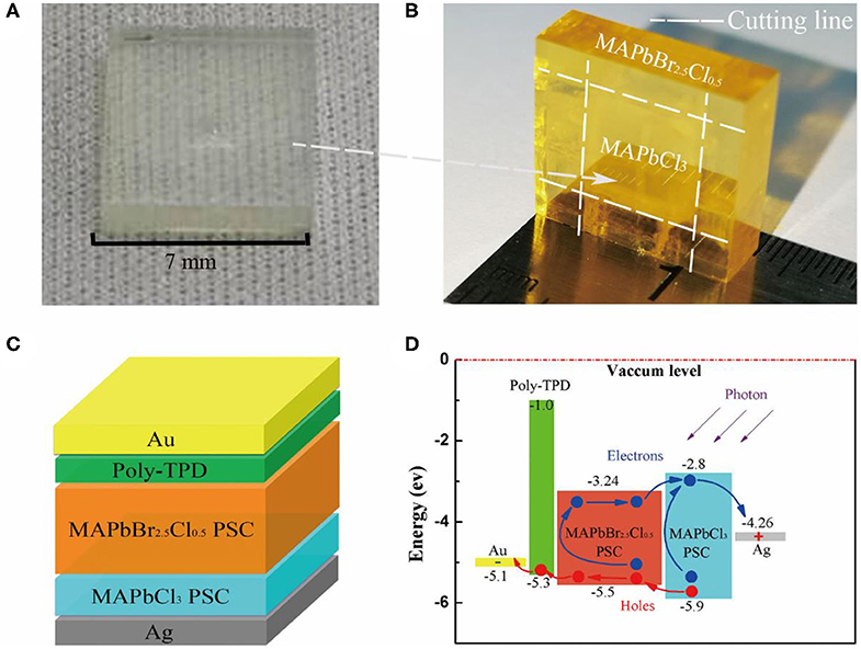
Figure 1. (A) Optical image of the colorless and transparent MAPbCl3 PSC grown by solution processes. (B) Optical image of the yellow MAPbBr2.5Cl0.5 enfolding the transparent MAPbCl3 PSC after epitaxy growth. (C) Schematic representation of the full photodiode structure after cutting the surrounding. (D) Energy level diagram of the PIN photodiode with epitaxial HBL.
Figure 1C shows the structure of the fabricated PIN photodiodes after cutting the surrounding, which is Au/poly-TPD/MAPbBr2.5Cl0.5 PSC/MAPbCl3 PSC/Ag. Poly-TPD serves as both HTL and EBL. MAPbCl3 PSC serves as both ETL and HBL (Sutherland and Sargent, 2016). Au and Ag function as the anode and cathode, respectively. The schematic energy level diagram of the PIN photodiode is shown in Figure 1D, in which the photo-generated electrons and holes in the active layer are effectively separated and transported to their corresponding electrodes under external electric field. Meanwhile, poly-TPD and MAPbCl3 PSC can effectively block the injected electrons and holes from the applied voltage source, respectively, benefiting the reduction of the dark current. The energy barriers of 4.1 eV and 1.64 eV between Au and poly-TPD and between MAPbCl3 PSC and Ag significantly reduce the injection of electrons and holes from the anode and cathode, respectively. The energy offset between poly-TPD and the conduction band minimum (CBM) of MAPbBr2.5Cl0.5 PSC is sufficiently large to block the transfer of electrons from MAPbBr3 PSC to the cathode.
To optimize the crystal surface, we utilized a diamond wire to saw off the extra surrounding of the MAPbBr2.5Cl0.5/MAPbCl3 heterojunction PSC bulk along the cutting lines shown in Figure 1B. The optical photograph of our PIN photodiode after machining the surrounding is shown in Figure 2A. The dimensions of our PIN photodiode are 7.28, 6.92, and 5.32 mm in length, width, and thickness, respectively. The effective electrode contact area is approximately (4.17 × 5.26 mm) 21.93 mm2. Moreover, the thicknesses of the MAPbBr2.5Cl0.5 intrinsic layer and MAPbCl3 HBL are approximately 2.41 and 2.91 mm, respectively.
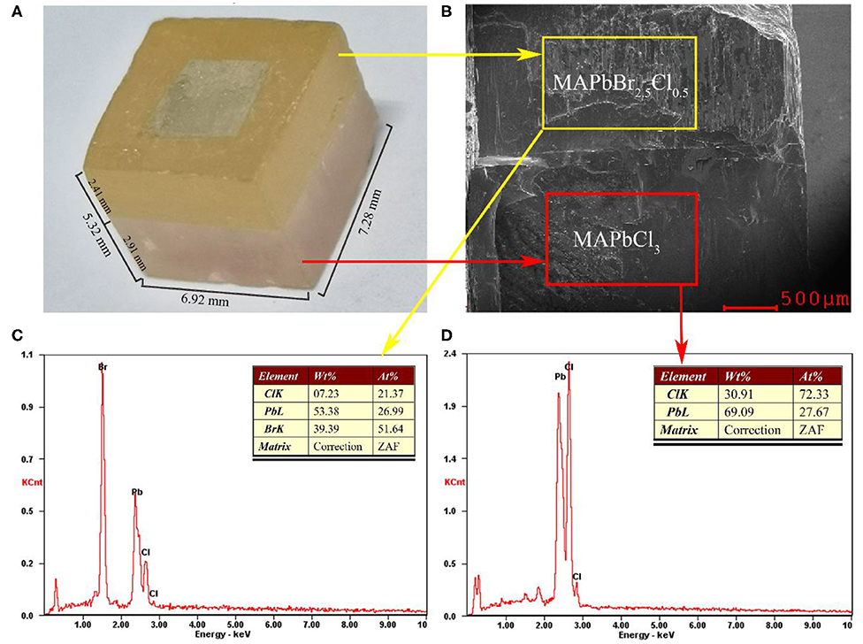
Figure 2. (A) Optical image of the epitaxial PIN device. (B) Cross-sectional SEM images of the double-layer perovskite bulk. EDX spectra of (C) epitaxial MAPbBr2.5Cl0.5 perovskite layer and (D) MAPbCl3 perovskite layer.
In this study, we have utilized energy dispersive X-ray (EDX) spectroscopy to investigate the lead and halide element distribution of MAPbCl3 PSC on epitaxial MAPbBr2.5Cl0.5. Figure 2B shows the cross-sectional scanning electron micrograph (SEM) image of the epitaxial perovskite bulk. Two parts of different halide content in the bulk are selected to analyze the EDX spectra. The EDX spectra of the epitaxial MAPbBr2.5Cl0.5 (areas outlined in yellow) and MAPbCl3 (areas outlined in red) are shown in Figures 2C,D, respectively. The ratios of the Pb, Br, and Cl elements in the two kinds of perovskite layers reveal a slight difference in the ratios of the precursor solution. This can be attributed to the considerable difference in the solubility of MABr/Cl and PbBr2/Cl2 in DMF (Wei et al., 2016).
The comparison between X-ray diffraction (XRD) patterns of MAPbCl3 PSC, MAPbBr2.5Cl0.5 PSC, and MAPbCl3 PSC on epitaxial MAPbBr2.5Cl0.5 are shown in Figure 3A. From the figure, the XRD spectra of the MAPbCl3 PSC on epitaxial MAPbBr2.5Cl0.5 is similar to the MAPbBr2.5Cl0.5 PSC but shifts slightly to larger angles, due to the combination of MAPbCl3 and MAPbBr2.5Cl0.5. The diffraction peaks in the XRD spectra correspond to the integer of the wavelength, which indicated the one crystalline structure of MAPbCl3 PSC on epitaxial MAPbBr2.5Cl0.5. The series of distinct characteristic peaks and small full width at half-maximum of the MAPbCl3 PSC on epitaxial MAPbBr2.5Cl0.5 indicate the high-quality crystallization. In addition, its diffraction peak positions nearly overlap with MAPbBr2.5Cl0.5 PSC and MAPbCl3 PSC, which corresponds to the reported graded heterojunction (Li et al., 2019b). The existence of main and secondary peaks in the XRD spectra of MAPbCl3 PSC on epitaxial MAPbBr2.5Cl0.5 is attributed to the diffraction of both thin epitaxial MAPbBr2.5Cl0.5 layer and MAPbCl3 layer.
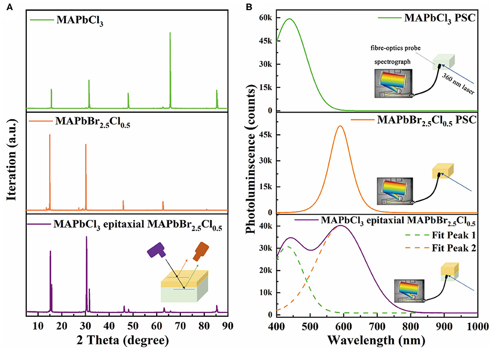
Figure 3. (A) XRD spectra and (B) PL spectra of MAPbCl3 PSC, MAPbBr2.5Cl0.5 PSC, and MAPbCl3 PSC on epitaxial MAPbBr2.5Cl0.5. Insets: the schematic diagram of PL spectra test.
The photoluminescence (PL) spectra of MAPbCl3 PSC, MAPbBr2.5Cl0.5 PSC, and epitaxial MAPbBr2.5Cl0.5 on MAPbCl3 block are displayed in Figure 3B. A 360-nm laser beam is used as the light source and incident on the surface of MAPbCl3 PSC, MAPbBr2.5Cl0.5 PSC, and the interface of the MAPbBr2.5Cl0.5-MAPbCl3 heterojunction. The PL peaks of MAPbCl3 PSC on epitaxial MAPbBr2.5Cl0.5 are similar to the stack of MAPbCl3 PSC and MAPbBr2.5Cl0.5 PSC. From this evidence, it can hereby be concluded that the MAPbBr2.5Cl0.5 PSC was successfully grown on the MAPbCl3 PSC.
To show the effects of reducing lattice mismatch between heterojunction interface by epitaxially combining another kind of PSC and the enhancement of the epitaxial PIN device performance, the spin-coating device with structure Au/poly-TPD/MAPbBr2.5Cl0.5 PSC/C60/PCBM/Ag was also fabricated for comparison.
The dark current density–voltage (J–V) characteristic curves of the epitaxial HBL device and spin-coated HBL device are shown in Figure 4A for comparison. The result indicates that the epitaxial HBL device shows lower dark current density than spin-coated HBL device in reverse voltage. At −250 V, the spin-coated device has a dark current density of 25 μA cm−2, which is only 2.9 μA cm−2 for the epitaxial HBL device. This indicates that the combination between the intrinsic layer and HBL by epitaxial growth contributes to the reduction of dark current. Furthermore, the dark current density of the epitaxial HBL device shows a value <100 nA cm−2 under −20 V, implying that the device has an advantage in the low dark current noise and large dynamic range.
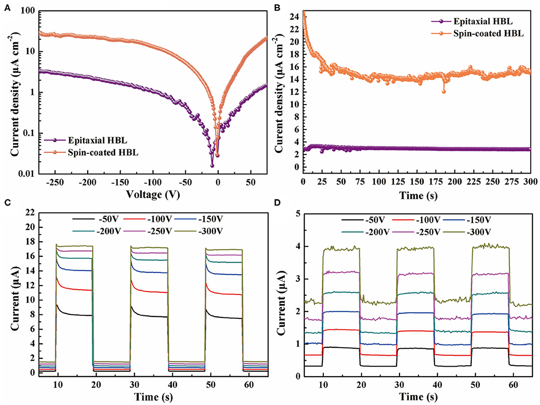
Figure 4. (A) Current density as a function of the voltage bias of the epitaxial HBL device and spin-coated HBL device in darkness. (B) Long-term dark current stability of the epitaxial HBL device and spin-coated HBL device. Temporal response of the photodiode based on (C) the epitaxial HBL device and (D) spin-coated HBL device under different voltage bias.
Figure 4B shows the long-term dark current stability of the epitaxial HBL device and spin-coated HBL device under −250 V reverse bias voltage. As shown in the figure, the dark current of the spin-coated HBL device declines quickly in 30 s after startup and takes place at relatively high amplitude fluctuations than the epitaxial HBL device, because the spin-coated organic molecular material is unstable under a high voltage. The amplitude of the vibrated dark current for the epitaxial HBL device is <40 nA cm−2 but more than 4 μA cm−2 for the spin-coated HBL device after 2 min. The more stable long-term dark current for the epitaxial HBL device can be attributed to the better lattice matched interface between the epitaxial HBL and MAPbBr2.5Cl0.5 PSC.
The photon detection performance is measured by a temporal photocurrent at −50 V, −100 V, −150 V, −200 V, −250 V, and −300 V, on 460-nm and 130-μW blue light illumination, as shown in Figures 4C,D. All the photo responses of the epitaxial HBL device are greater than the spin-coated HBL device under different bias voltages. The rise of the photo response rate is higher than dark currents for the epitaxial HBL device with increasing bias voltage. The responsivities of the epitaxial HBL device are calculated as:
where P is incident optical power, which is 58.7 mA W−1, 81.7 mA W−1, 98.6 mA W−1, 112 mA W−1, 117 mA W−1, and 122 mA W−1 from −50 to −300 V, respectively. The larger responsivity is caused by the decrease of carrier recombination on the MAPbCl3/MAPbBr2.5Cl0.5 heterojunction interface.
Response speed is a significant factor for photodiodes that are applied in detection and imaging. In this study, a 365-nm pulsed laser with 7 ns pulse width at 20 Hz frequency is used as an excitation light source to measure the decay process of the photocurrent that reflects the detection speed of the device. Figures 5A,B show the decay process of the photodiodes with epitaxial HBL and spin-coated HBL, having 5.3 and 3.2 mm thickness, respectively, under −250 V bias. The fall time defined as decaying to e−1 of the maximum for different devices are measured as 10 and 15 μs, respectively, which signify that the photodiode with epitaxial HBL has a faster detection speed. Subsequently, the carrier mobilities of the epitaxial HBL and spin-coated devices are measured using the time of flight (TOF) technique. The average charge-carrier mobilities of the epitaxial HBL and spin-coated HBL devices are measured by the 365-nm nanosecond laser illuminated from the Au electrode side. The transient time for electron carrier transport through the whole perovskite device was used for average electron mobility calculation according to the formulation (Wei et al., 2016; Thirimanne et al., 2018; Hu et al., 2020):
where μ is the mobility, d is the thickness of the device, τ is the transmit time, and V is the bias voltage. The transient photocurrent responses of the epitaxial device and spin-coated device under different bias voltages were recorded and are shown in Figures 5C,D. By fitting the plot of τ-V−1, as shown in the insets, the calculated results reveal that the average electron mobility of the spin-coated HBL device is 188 cm2 V−1 s−1 while that of the epitaxial HBL device is 386 cm2 V−1 s−1. The epitaxial HBL device has better average electron mobility than the spin-coated HBL device, which is attributed to the substitution low surface trap single crystals for additional solution-processed layers. A detailed comparison of our epitaxial HBL perovskite photodetector with the reported layered perovskite-based photodetectors is summarized in Table 1.
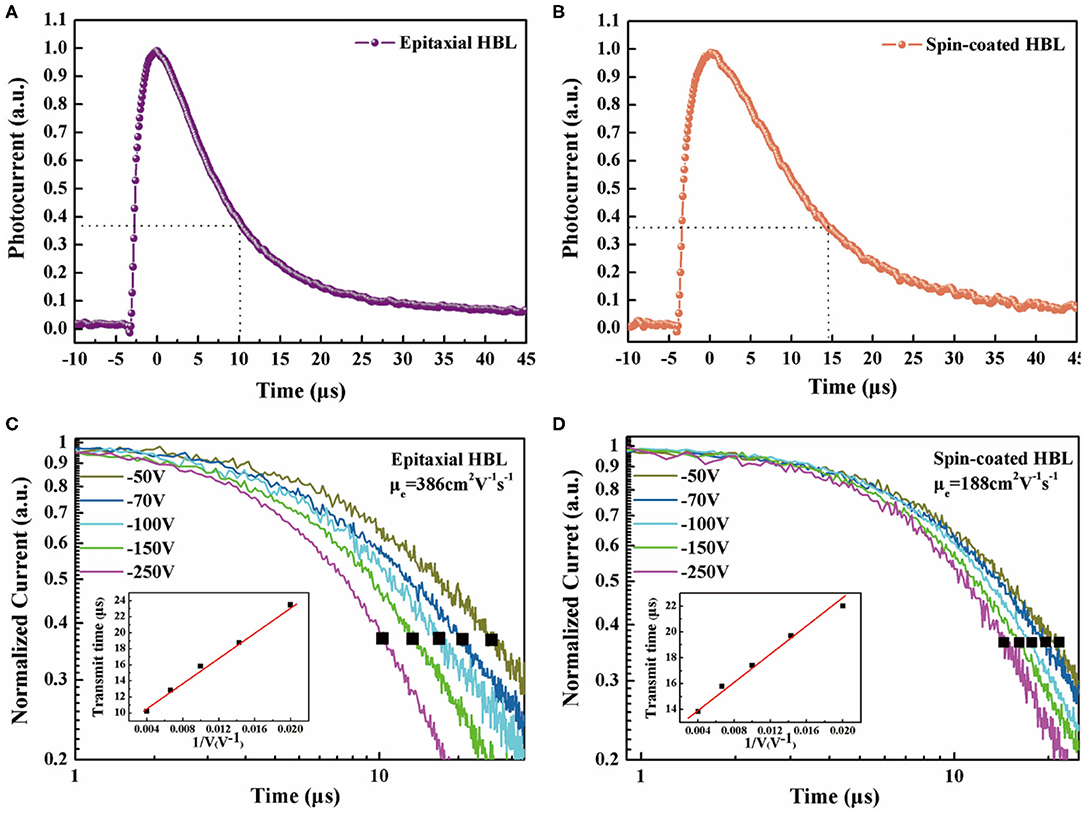
Figure 5. Normalized transient current response of the (A) epitaxial EBL device and (B) spin-coated EBL device. Decay curve of the (C) epitaxial EBL device and (D) spin-coated EBL device. Insets: electron transmit time vs. the reciprocal of bias (the solid line is a linear fit to the data).
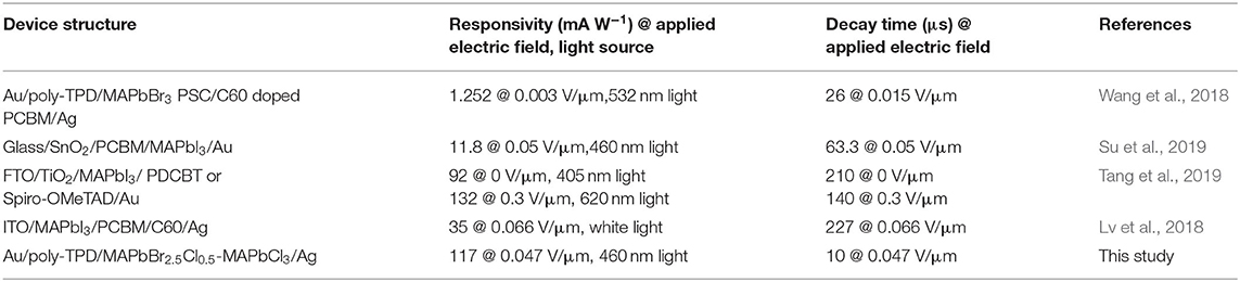
Table 1. Comparison of the epitaxial HBL perovskite photodetector with the reported layered perovskite photodetectors.
Furthermore, other key parameters of our epitaxial photodiode were also measured. When light beam with wavelength that varies continuously is incident on the cathode of the photodiode with epitaxial HBL, its responsivity spectra under different voltages are shown in Figure 6A. The results show a few smaller responsivity than that of temporal response in Figure 4C because incident light was partially obscured by the thick Ag electrode. The photodiode is most sensitive at 430 and 500 nm but almost insensitive for photons with wavelength exceeding 540 nm. With the increase of reverse voltage, the responsivity improves significantly. This is due to the different band gap for MAPbCl3 PSC and MAPbBr2.5Cl0.5 PSC, i.e., 3.1 and 2.26 eV, respectively. In addition, short-wave photons generate a higher current response (2.26 mA W−1 at 430 nm, 1.54 mA W−1 at 510 nm) under low-bias voltage (−10 V). However, long-wave photons generate a higher current response (12.24 mA W−1 at 430 nm, 16.73 mA W−1 at 500 nm) under high-bias voltage (−100 V). This is because electron–hole pairs are generated at a deeper depth inside the active layer with the increase of the incident photon wavelength. Electron–hole pairs at different depths have been collected by applying different reverse voltages. The collection efficiency has also been improved with increase of the applying voltage. The noise current (In) of the epitaxial device under −100 V is measured as 1.12 × 10⁻¹⁰ A Hz−1/2 approximately. Based on the In and R, the specific detectivity (D*) of the epitaxial device could be obtained by the following equations (Li et al., 2020):
where A is the active layer area and f is the bandwidth. The results of D* value is similar to the trend of R (Li et al., 2019a). The maximum D* of the epitaxial device is calculated about 7.32 × 107 cm Hz1/2 W−1 at 500 nm under −100 V. The external quantum efficiency (EQE) of the epitaxial device under −100 V at 500 nm is calculated as about 4.5% by the following equations:
where h is Plank's constant, c is the velocity of light, q is the absolute value of the electron charge, and λ is the light wavelength.
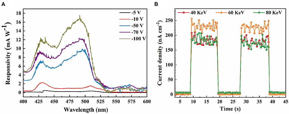
Figure 6. (A) Responsivity spectra of the epitaxial PIN device under different voltage bias. (B) Temporal response of the epitaxial PIN device at 0 V bias with different energy X-rays on and off.
Due to the thickness of the epitaxial photodiode in the solution process being suitable for the potential application of X-ray detection, the X-ray detection performance under zero bias is also investigated in this work. Photocurrents caused by 40-keV, 60-keV, and 80-keV X-ray photons with a dose rate 27.91 μGyair s−1, 62.03 μGyair s−1, and 84.89 μGyair s−1, respectively, are shown in Figure 6B. The 5.32-mm-thick device with epitaxial EBL with self-powered shows a satisfactory response to the 40-keV, 60-keV, and 80-keV X-ray photons due to the built-in electric field of the PIN device. The X-ray detection sensitivities (S) of the epitaxial HBL device are calculated as:
where Q is the collected photo charge, A is the effective detection area, and X is the radiation dose, which is 7.08 × 10³ μC Gyair−1 cm−2, 4.04 × 10³ μC Gyair−1 cm−2, and 2.38 × 10³ μC Gyair−1 cm−2 for the 40-, 60-, and 80-keV X-ray photons, respectively. The sensitivity of our epitaxial device with self-powered is superior to the majority of hybrid perovskite film and single crystalline device, such as MAPbI3 film device (25 μC Gyair−1 cm−2) (Yakunin et al., 2015), CsPbBr3 thick film device (0.27–1.7 × 10³ μC Gyair−1 cm−2) (Gou et al., 2019), and MAPbBr3 single crystalline device (80 μC Gyair−1 cm−2) (Wei et al., 2016). Moreover, the sensitivity of our epitaxial device with self-powered is stronger than that of the currently commercial detectors such as a-Se, CdZnTe, HgI2, and PbI2 working at a much higher field (Schieber et al., 2001). The results reveal the advantage of the application of our epitaxial PIN photodiode for X-ray detection.
Conclusion
To summarize, heterojunction bulk PSC has been fabricated based on liquid-phase epitaxial MAPbBr2.5Cl0.5 on MAPbCl3 PSC. A 10-fold reduction of the dark current is achieved for the PIN photodiode with epitaxial HBL in comparison to the photodiode fabricated by spin-coated additional organic n-type semiconductor materials as HBL. Additionally, the epitaxial HBL device also shows greater responsivity, better stability, faster response time to 10 μs, and a higher average charge-carrier mobility up to 386 cm2 V−1 s−1 than the spin-coated HBL device. The device also reveals a satisfactory detection sensitivity up to several mC Gyair−1 cm−2 for 40- to 80-keV X-ray photons. This research proves that epitaxial growth is a more reliable, effective method to fabricate perovskite–perovskite heterojunctions and can avoid lattice mismatch on the interface. Hence, the use of epitaxial PSC HBL to form heterojunction interface can be a promising method for the fabrication of high-performance perovskite photodiode devices.
Data Availability Statement
The raw data supporting the conclusions of this article will be made available by the authors, without undue reservation.
Author Contributions
YP, XW, and YX grew the perovskite single crystals. YP conducted the epitaxial experiments and wrote this manuscript. YP and YL conducted the measurements. XW and YP analyzed the results. All authors have made comments on the manuscript.
Funding
This work was supported by the National Key R&D Program of China (Grant Nos. 2017YFC0111500 and 2016YFB0401600), the National Natural Science Foundation Project (Grant Nos. 61775034, 61571124, and 61674029), and the International Cooperation Program of Jiangsu Province (Grant No. BZ2018056).
Conflict of Interest
The authors declare that the research was conducted in the absence of any commercial or financial relationships that could be construed as a potential conflict of interest.
References
Chen, Z., Du, X., Zeng, Q., and Yang, B. (2017). Recent development and understanding of polymer–nanocrystal hybrid solar cells. Mater. Chem. Front. 1, 1502–1513. doi: 10.1039/C7QM00022G
Cheng, X., Yang, S., Cao, B., Tao, X., and Chen, Z. (2019). Single crystal perovskite solar cells: development and perspectives. Adv. Funct. Mater. 30:1905021. doi: 10.1002/adfm.201905021
Dai, X., Zhang, Z., Jin, Y., Niu, Y., Cao, H., Liang, X., et al. (2014). Solution-processed, high-performance light-emitting diodes based on quantum dots. Nature 515, 96–99. doi: 10.1038/nature13829
Fang, Y., and Huang, J. (2015). Resolving Weak Light of Sub-picowatt per Square Centimeter by Hybrid Perovskite Photodetectors Enabled by Noise Reduction. Adv. Mater. 27, 2804–2810. doi: 10.1002/adma.201500099
Gill, H. S., Elshahat, B., Kokil, A., Li, L., Mosurkal, R., Zygmanski, P., et al. (2018). Flexible perovskite based X-ray detectors for dose monitoring in medical imaging applications. Phys. Med. 5, 20–23. doi: 10.1016/j.phmed.2018.04.001
Gou, Z., Huanglong, S., Ke, W., Sun, H., Tian, H., Gao, X., et al. (2019). Self-powered X-ray detector based on all-inorganic perovskite thick film with high sensitivity under low dose rate. Phys. Status Solidi Rapid Res. Letters 13:1900094. doi: 10.1002/pssr.201900094
Hu, M., Jia, S., Liu, Y., Cui, J., Zhang, Y., Su, H., et al. (2020). Large and dense organic-inorganic hybrid perovskite CH3NH3PbI3 wafer fabricated by one-step reactive direct wafer production with high x-ray sensitivity. ACS Appl. Mater. Interfaces 12, 16592–16600. doi: 10.1021/acsami.9b23158
Jara, D. H., Yoon, S. J., Stamplecoskie, K. G., and Kamat, P. V. (2014). Size-dependent photovoltaic performance of CuInS2 quantum dot-sensitized solar cells. Chem. Mater. 26, 7221–7228. doi: 10.1021/cm5040886
Jiang, S., Wang, X., Wu, Y., Li, Y., Zhang, Q., Li, G., et al. (2019). Balance lead in solution-processed CH3NH3PbBrxCl(3–x) single crystals for high performance X-ray detection. Mater. Lett. 236, 26–29. doi: 10.1016/j.matlet.2018.10.055
Ju, M.-G., Chen, M., Zhou, Y., Dai, J., Ma, L., Padture, N. P., et al. (2018). Toward eco-friendly and stable perovskite materials for photovoltaics. Joule 2, 1231–1241. doi: 10.1016/j.joule.2018.04.026
Kojima, A., Miyasaka, T., Teshima, K., and Shirai, Y. (2009). Organometal halide perovskites as visible-light sensitizers for photovoltaic cells. J. Am. Chem. Soc. 131, 6050–6051. doi: 10.1021/ja809598r
Li, C., Lu, J., Zhao, Y., Sun, L., Wang, G., Ma, Y., et al. (2019a). Highly sensitive, fast response perovskite photodetectors demonstrated in weak light detection circuit and visible light communication system. Small 15:e1903599. doi: 10.1002/smll.201903599
Li, C., Wang, H., Wang, F., Li, T., Xu, M., Wang, H., et al. (2020). Ultrafast and broadband photodetectors based on a perovskite/organic bulk heterojunction for large-dynamic-range imaging. Light Sci. Appl. 9:31. doi: 10.1038/s41377-020-0264-5
Li, W.-G., Wang, X.-D., Liao, J.-F., Wei, Z.-F., Xu, Y.-F., Chen, H.-Y., et al. (2019b). A laminar MAPbBr3/MAPbBr3–xIx graded heterojunction single crystal for enhancing charge extraction and optoelectronic performance. J. Mater. Chem. C 7, 5670–5676. doi: 10.1039/C9TC00972H
Lin, Q., Armin, A., Lyons, D. M., Burn, P. L., and Meredith, P. (2015). Low noise, IR-blind organohalide perovskite photodiodes for visible light detection and imaging. Adv. Mater. 27, 2060–2064. doi: 10.1002/adma.201405171
Liu, D., and Kelly, T. L. (2014). Perovskite solar cells with a planar heterojunction structure prepared using room-temperature solution processing techniques. Nat. Photonics 8, 133–138. doi: 10.1038/nphoton.2013.342
Lv, Q., Lian, Z., He, W., Sun, J.-L., Li, Q., and Yan, Q. (2018). A universal top-down approach toward thickness-controllable perovskite single-crystalline thin films. J. Mater. Chem. C 6, 4464–4470. doi: 10.1039/C8TC00842F
Malinkiewicz, O., Yella, A., Lee, Y. H., Espallargas, G. M. n., Graetzel, M., et al. (2014). Perovskite solar cells employing organic charge-transport layers. Nat. Photonics 8, 128–132. doi: 10.1038/nphoton.2013.341
Ou, Q., Bao, X., Zhang, Y., Shao, H., Xing, G., Li, X., et al. (2019). Band structure engineering in metal halide perovskite nanostructures for optoelectronic applications. Nano Mater. Sci. 1, 268–287. doi: 10.1016/j.nanoms.2019.10.004
Schieber, M., Hermon, H., Zuck, A., Vilensky, A., Melekhov, L., Shatunovsky, R., et al. (2001). Thick films of X-ray polycrystalline mercuric iodide detectors. J. Crystal Growth 225, 118–123. doi: 10.1016/S0022-0248(01)00832-6
Su, H., Meng, L., Liu, Y., Zhang, Y., Hu, M., Yang, Z., et al. (2019). Effective electron extraction from active layer for enhanced photodetection of photoconductive type detector with structure of Au/CH3NH3PbI3/Au. Org. Electron 74, 197–203. doi: 10.1016/j.orgel.2019.06.015
Sutherland, B. R., and Sargent, E. H. (2016). Perovskite photonic sources. Nat. Photonics 10, 295–302. doi: 10.1038/nphoton.2016.62
Tan, Z.-K., Moghaddam, R. S., Lai, M. L., Docampo, P., Higler, R., Deschler, F., et al. (2014). Bright light-emitting diodes based on organometal halide perovskite. Nat. Nanotechnol. 9, 687–692. doi: 10.1038/nnano.2014.149
Tang, X. F., Matt, G. J., Gao, S., Gu, E., Almora, O., and Brabec, C. J. (2019). Electrical-field-driven tunable spectral responses in a broadband-absorbing perovskite photodiode. ACS Appl. Mater. Interfaces 11, 39018–39025. doi: 10.1021/acsami.9b14788
Thirimanne, H. M., Jayawardena, K., Parnell, A. J., Bandara, R. M. I., Karalasingam, A., Pani, S., et al. (2018). High sensitivity organic inorganic hybrid X-ray detectors with direct transduction and broadband response. Nat. Commun. 9:2926. doi: 10.1038/s41467-018-05301-6
Wang, H., and Kim, D. H. (2017). Perovskite-based photodetectors: materials and devices. Chem. Soc. Rev. 46, 5204–5236. doi: 10.1039/C6CS00896H
Wang, J., Wang, N., Jin, Y., Si, J., Tan, Z.-K., Du, H., et al. (2015). Interfacial control toward efficient and low-voltage perovskite light-emitting diodes. Adv. Mater. 27:2311. doi: 10.1002/adma.201405217
Wang, X., Huang, Y., Lei, W., Li, Q., Zhang, X., Khan, Q., et al. (2017). Asymmetrical photodetection response of methylammonium lead bromide perovskite single crystal. Crystal Res. Technol. 52:5. doi: 10.1002/crat.201700115
Wang, X., Wu, Y., Li, G., Li, Y., Wu, J., Zhang, X., et al. (2019). Fabrication of photodiodes based on solution-processed perovskite single crystals. IEEE Trans. Electron Devices 66, 485–490. doi: 10.1109/TED.2018.2878828
Wang, X., Zhao, D., Qiu, Y., Huang, Y., Wu, Y., Li, G., et al. (2018). PIN diodes array made of perovskite single crystal for X-ray imaging. Phys. Status Solidi Rapid Res. Letters 12:7. doi: 10.1002/pssr.201800380
Wei, H., Fang, Y., Mulligan, P., Chuirazzi, W., Fang, H.-H., Wang, C., et al. (2016). Sensitive X-ray detectors made of methylammonium lead tribromide perovskite single crystals. Nat. Photonics 10, 333–339. doi: 10.1038/nphoton.2016.41
Yakunin, S., Sytnyk, M., Kriegner, D., Shrestha, S., Richter, M., Matt, G. J., et al. (2015). Detection of X-Ray Photons by Solution-Processed Lead Halide Perovskites. Great Britain: Nature Publishing Group. doi: 10.1038/nphoton.2015.82
Zeng, X., Zhou, T., Leng, C., Zang, Z., Wang, M., Hu, W., et al. (2017). Performance improvement of perovskite solar cells by employing a CdSe quantum dot/PCBM composite as an electron transport layer. J. Mater. Chem. A 5, 17499–17505. doi: 10.1039/C7TA00203C
Keywords: perovskite single crystals, heterojunction, PIN diodes, epitaxial growth, photoelectric detection
Citation: Pan Y, Wang X, Xu Y, Li Y, Elemike EE, Shuja A, Li Q, Zhang X, Chen J, Zhao Z and Lei W (2020) Enhanced Performance of Perovskite Single-Crystal Photodiodes by Epitaxial Hole Blocking Layer. Front. Chem. 8:791. doi: 10.3389/fchem.2020.00791
Received: 30 March 2020; Accepted: 28 July 2020;
Published: 10 September 2020.
Edited by:
Zhaolai Chen, Shandong University, ChinaReviewed by:
Andrew Nattestad, University of Wollongong, AustraliaLiang Shen, Jilin University, China
Copyright © 2020 Pan, Wang, Xu, Li, Elemike, Shuja, Li, Zhang, Chen, Zhao and Lei. This is an open-access article distributed under the terms of the Creative Commons Attribution License (CC BY). The use, distribution or reproduction in other forums is permitted, provided the original author(s) and the copyright owner(s) are credited and that the original publication in this journal is cited, in accordance with accepted academic practice. No use, distribution or reproduction is permitted which does not comply with these terms.
*Correspondence: Xin Wang, MjMwMTU5NDI0QHNldS5lZHUuY24=; Wei Lei, bHdAc2V1LmVkdS5jbg==