 Yu Zhang1,2
 Xiong Chen1,2
 Hao Zhang1,2*Shaozu Hu1Guohong Zhao1Meifang Zhang1Wei Qin1Zhaohua Wang1Xiaowei Huang1Jun Wang3*
- 1Organic Optoelectronics Engineering Research Center of Fujian's Universities, College of Electronics and Information Science, Fujian Jiangxia University, Fuzhou, China
- 2Fujian Innovation Center of Additive Manufacturing, Fuzhou, China
- 3College of Science, Shanghai Institute of Technology, Shanghai, China
Molybdenum disulfide (MoS2), a typical member of the transition metal dichalcogenides (TMDs) group, is known for its excellent electronic performance and is considered a candidate next-generation semiconductor. The preparation of MoS2 nanoflakes for use as the core of semiconducting devices depends on mechanical exfoliation, but its quality has not yet been optimized. In this paper, a novel exfoliation method of achieving MoS2 nanoflakes is proposed. We find that the size and yield of the exfoliated flakes are improved after thermal treatment for 2 h at a temperature of 110°C followed by precooling for 10 min in ambient air. The new method has the advantage of a 152-fold larger size of obtained MoS2 flakes than traditional mechanical exfoliation. This phenomenon may be attributable to the differences in van Der Waals force and the increase in surface free energy at the interface induced by thermal treatment. In addition, a field-effect transistor (FET) was fabricated on the basis of multilayer MoS2 prepared according to a new process, and the device exhibited a typical depleted-FET performance, with an on/off ratio of ~105 and a field-effect mobility of 24.26 cm2/Vs in the saturated region when VG is 10 V, which is generally consistent with the values for devices reported previously. This implies that the new process may have potential for the standard preparation of MoS2 and even other 2D materials as well.
Introduction
The era of two-dimensional (2D) materials was initiated with the birth of graphene exfoliated from graphite using Scotch tape by Novoselov et al. (2004). These materials incorporate flake-like structures with a lateral size from 100 nm up to a few micrometers and a thickness that is typically on the scale of a nanometer, a single or only a few layers of atoms (Zhang, 2015). Over the last decade, more members of the 2D-material family, including black phosphorus (Cartz et al., 1979; Zhang X. et al., 2015), hexagonal boron nitride (Lin et al., 2010; Weng et al., 2016), graphitic carbon nitride (g-C3N4) (Zhang J. et al., 2015; Ong et al., 2016), and transition metal dichalcogenides (TMDs) (Huang et al., 2013; Lv et al., 2015; Tan and Zhang, 2015) have been developed and explored in depth.
A TMDs is a type of 2D material that consists of a transition metal element (e.g., Mo, W) and a chalcogen (e.g., S, Se) (Wilson and Yoffe, 1969; Beal et al., 1972; Qiu et al., 2012). As a semiconductor material for TMDs, molybdenum disulfide (MoS2) is known for its special direct–indirect bandgap widths of 1.8 and 1.3 eV, respectively (Mak et al., 2012), high field-effect mobility (Radisavljevic et al., 2011) in electronic devices, and inner structure of single or multiple atomic layers, which may exhibit significant promise in the application of high-performance, flexible electronic devices.
The first step in preparing devices based on MoS2 is to transfer the material to certain substrates. The methods for this can be divided into two categories, namely, “top to bottom” and “bottom to top.” The process for the former is mainly executed by making the bulk into flake through methods such as micromechanical exfoliation (Novoselov et al., 2004; Nicolosi et al., 2013; Li et al., 2014; Yi and Shen, 2015; Niu et al., 2016) and liquid exfoliation assisted by ion intercalation (Dines, 1975; Joensen et al., 1986). The latter is achieved by depositing the atomic layer on the substrate using one of several techniques, including chemical vapor deposition (Liu et al., 2005; Wu et al., 2013) and atomic-layer deposition (Riikka, 2005; Jin et al., 2014). Mechanical exfoliation is currently considered a relatively ideal way to achieve nanoflakes of 2D materials for a free-contamination, crystalline product in a way that is independent of equipment. However, due to the non-standardized and uncontrollable process used, high-quality 2D nanoflakes with large areas and yields are more difficult to obtain using mechanical exfoliation. Some studies have been conducted to improve this process. For example, Desai et al. demonstrated an exfoliation technique using evaporated gold films to exfoliate large-area TMD monolayers onto various substrates, such as SiO2/Si and quartz (Desai et al., 2016). Huang et al. introduced a universal Au-assisted method of mechanical exfoliation and demonstrated its effectiveness by exfoliating MoS2 monolayers (Huang et al., 2020). However, these methods must be carried out with some other materials, which have to be removed with solvents, leading to contamination at the interface. Furthermore, multilayer TMDs offer higher drive currents from multiple conducting channels than monolayer TMD channels, with a higher density of states as well as lower sensitivity to charge impurities at the interface, better immunity against noise in air, and greater ability to form large-size nanoflakes (Kim et al., 2012; Kwon H. et al., 2014; Kwon H. J. et al., 2014).
In this work, we report a method for preparing MoS2 nanoflakes based on mechanical exfoliation through thermal treatment without assistance. In this way, the values for the number of samples that reach a specific size were executed to estimate the effects and achieve ideal parameters for the new process. Subsequently, we characterized the flake samples according to Raman spectra and atomic force microscopy (AFM). We confirmed that thermal treatment can clearly improve the size and yield of MoS2 nanoflakes. This approach is a prominent means of preparing 2D-layered materials. Furthermore, to explore the application of this novel means of materials preparation, a field-effect transistor (FET) was fabricated, using multilayer-thick MoS2 flakes exfoliated after thermal treatment. The field-effect mobility of the device is 24.26 cm2/Vs in the saturated region, and the on/off ratio is ~105. These results are consistent with those of devices reported previously, which implies the applicability of the new nanoflake-preparation method.
Materials and Methods
MoS2 was purchased in bulk from a 2D semiconductor manufacturer. The substrates were formed from two parts. The upper was 300 nm thermal oxygenized SiO2, and the lower was highly doped n-type Si. The Scotch tape used to dissociate the bulk into flakes was purchased from a 3M Company.
The MoS2 nanoflakes were prepared as follows (Figure 1). First, the substrate was ultrasonically cleaned with acetone and isopropanol for 20 min to reduce contamination. Second, we reduced the bulk of the MoS2 by transferring it from the original tape to four others. The last transferred tape was placed to cover the substrate, and the MoS2 was in contact with the SiO2 layer. We repeatedly pressed the surface of the tape with the thumb for about 20 s to ensure relatively close contact. Then thermal treatment was carried out under the wafer for a period of time. Eventually, we removed the tapes from the substrate using direct or precooling exfoliation.
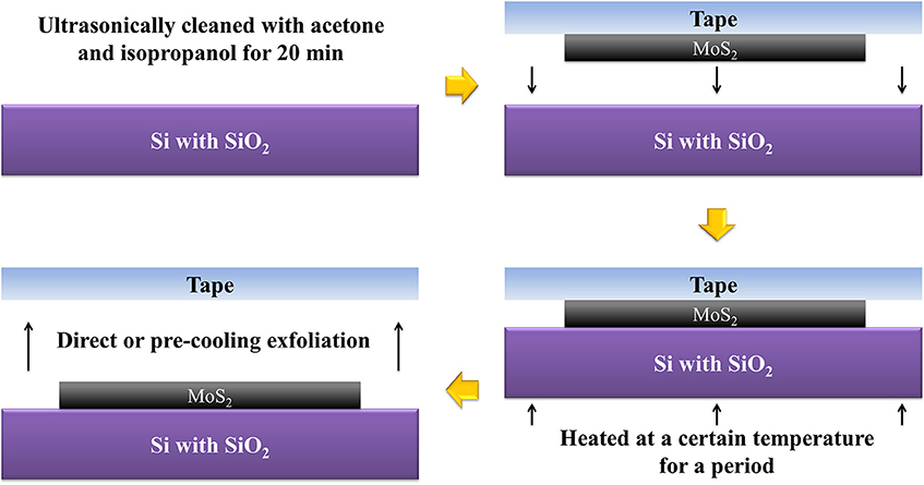
Figure 1. Preparation of MoS2 nanoflakes by thermal treatment.
Following the above procedures, we utilized MoS2 nanoflakes on Si/SiO2 substrates as an active layer and Ag as drain-source electrodes to fabricate FETs. Here, the drain-source electrodes were formed using shadow masking and vacuum vapor deposition.
To explore the influence of temperature on the size and quantity of the flake product, we prepared 48 Si/SiO2 substrates and divided them into eight batches on average (six per batch). Then, with the MoS2 bulk sticking to the substrates with the tape, thermal treatment was carried out for 5 h at eight temperatures, from 35 to 140°C (at intervals of 15°C), corresponding to the eight batches of Si/SiO2 substrates with MoS2 bulk, as mentioned above. At the end of the thermal treatment, we obtained MoS2 nanoflakes in two ways, through direct or precooling exfoliation after heating. Each method was applied to three bulk-on-substrate samples per batch; see Figure 2A.
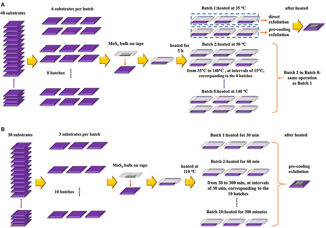
Figure 2. Processes of (A) temperature-dependent and (B) time-dependent experiments.
To clarify the effects of heating time on flake quality, we prepared 30 Si/SiO2 substrates and divided them into 10 batches (three per batch). Subsequently, the substrates were heated at 110°C for different periods of time, from 30 to 300 min, at intervals of 30 min, corresponding to the 10 batches, as shown in Figure 2B. After thermal treatment, we exfoliated the tapes from the wafer, followed by pre-cooling for 10 min.
The characterization of the samples above was conducted using various instruments, as described below. The spectra of the flakes were analyzed with Raman spectrometers (model: RENISHAW inVia) and photoluminescence spectrometers (model: Edinburgh FS5). The electrical performance of the MoS2-FET was tested using semiconductor parameter analyzers (model: Keithley 4200). The micro-images of the samples were taken with an optical microscope (model: LEIKA DM2700M) and an atomic force microscope (model: HITACHI-AFM5000II), and the contact angles of interfaces were measured using a contact angle meter (model: KINO SL200KS).
Results and Discussion
Statistical Analyses Based on Microimages
First, we observed the microimages of MoS2 nanoflakes with an optical microscope and counted the number of flakes with sizes of 1.2 × 10⁵, 2.0 × 10⁴, and 5.0 × 103 μm2 on each substrate, corresponding to the temperature-dependent experiment (Figure 2A). As mentioned above, a batch of bulk-on-substrate samples were heated at temperatures from 35 to 140°C (increasing at intervals of 15°C) for 5 h. We then separated the samples in each batch into two halves. Three were exfoliated immediately, and the other three were separated after precooling for 10 min to obtain MoS2 flakes. The statistics for the average amount of flakes on the substrates for different heating temperatures are shown in Figures 3A,B. The values shown in the panels are relative to the results of direct or precooling exfoliation after heating, respectively. From these two figures, we found that the quantity of flakes that reaches a certain size was higher at 110°C in both direct and precooling exfoliation. The precooling method presented a greater number of MoS2 flakes than direct exfoliation. Thus, we concluded that exfoliation with precooling after heating at 110°C for 5 h is a suitable means of improving the yield of MoS2 flakes. Furthermore, according to the description given in section two, in the time-dependent experiment, 30 bulk-on-substrate samples were divided into 10 batches, with heating times from 30 to 300 min (increased by 30 min). The average amount for each batch of MoS2 nanoflakes reaching the sizes of 1.2 × 10⁵, 2.0 × 10⁴, and 5.0 × 103 μm2 after precooling exfoliation at 110°C is presented in Figure 4. This shows that the size and yield of the flakes after heating for 120 min is generally high.
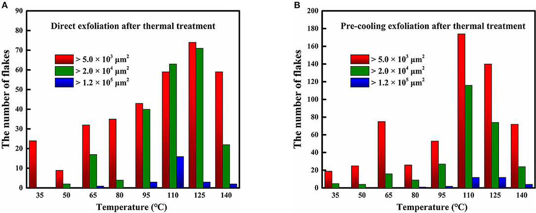
Figure 3. Quantity of certain MoS2 nanoflakes prepared by (A) direct and (B) pre-cooling exfoliation after thermal treatment for 5 h.
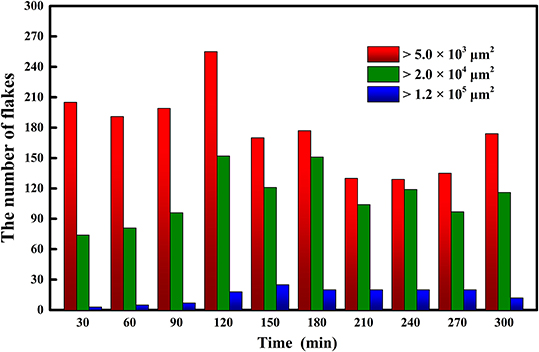
Figure 4. Statistics of MoS2 nanoflakes prepared with pre-cooling exfoliation after thermal treatment at different durations.
From the above phenomena, we can confirm that the most suitable way to prepare MoS2 nanoflakes in our experimental range is to treat the wafer with MoS2 bulk for 2 h at 110°C and then exfoliate the bulk after precooling for 10 min. A comparison with traditional exfoliation without any aid indicated that the size and yield of the flakes showed obvious improvement, as seen in Figures 5A,B. Statistical evaluation showed that through the heating process at 110°C for 2 h, 152 flakes were obtained that were larger than 2 × 104 μm2, while only one was obtained through original mechanical exfoliation, as shown in Figure 5C. This characterization indicates that the quantity of flakes significantly improved in the thermal treatment process, compared with traditional mechanical exfoliation, which can be attributed to two factors, as shown in Figure 6.
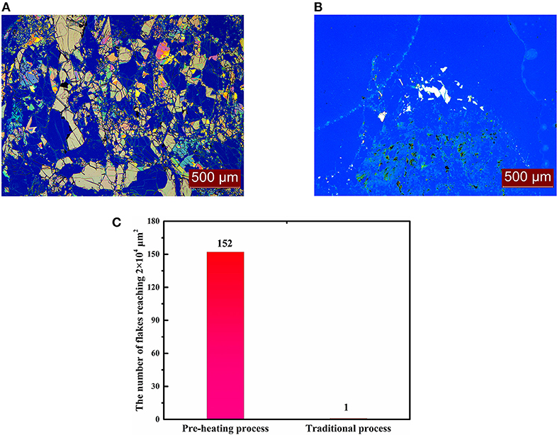
Figure 5. Microimages of MoS2 nanoflakes exfoliated by (A) pre-heating and (B) traditional processes and (C) their statistics.
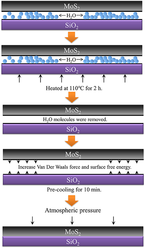
Figure 6. Mechanisms of exfoliation based on thermal treatment.
First, heating at 110°C for 120 min leads to complete evaporation of the water between the MoS2 and the wafer. This mechanism plays a critical role in the adequate adhesion of the interface, with the help of atmospheric pressure. The van der Waals force of the interface may then be greater than the interlamination of the MoS2 bulk. In this way, the bulk can easily be dissociated into nanoflakes on the SiO2 substrate. It must be mentioned that the boiling point of water is generally considered to be 100°C, but considering the heat lost in thermal radiation and conduction, the actual heating temperature must be higher than 100°C and remain there for some time to ensure the complete evaporation of water at the interface. It can be shown by statistics that the quantity of MoS2 nanoflakes obtained at the heating temperature of 110°C is larger than that at 100°C.
Next, precooling before exfoliation may result in a difference in temperature between the surface and interior of the bulk. Higher temperatures cause a violent movement of molecules that may weaken the van der Waals force of the interlayer in the bulk. Furthermore, the van der Waals force between the MoS2 and the wafer is increased by the decreases in the temperature outside. Thus, a difference in van der Waals force appears, which is beneficial for the preparation of the MoS2 flakes through easier exfoliation from bulk.
The surface free energy (SFE) is a measure of the destruction of chemical bonds between molecules when creating a material surface. According to solid-state physical theory, surface atoms have more energy than internal atoms for the interruption of chemical bonds on the surface. According to the law of conservation of energy, a higher SFE of the substrate has the potential to be reduced through adsorption of other molecules or atoms around it. Here, the adsorption capacity of the solid surface to the materials in contact is improved (Dong et al., 2010). We tested the contact angle on the substrate treated at the temperatures 35, 50, 65, 80, 95, 110, 125, and 140°C. We then extracted the value of the SFE of substrates through a reformulation of the equation of state for the interfacial tensions proposed by Li and Neumann (1990) (see Equations 1 and 2), where γsl, γsv, and γlv represent the SFE of the solid and liquid interface, the solid SFE, and the liquid SFE, respectively; θ is the contact angle between the solid surface and liquid; and β is an empirical value, namely, 1.247 × 10⁻⁴. The calculated results are as shown in Table 1, and they demonstrate that the maximum SFE of the substrates occurs at the temperature of 110°C, which is consistent with our previous experiment. This indicates that thermal treatment at 110°C should also lead to an increase in SFE on the substrates, which further improves the quality of the exfoliated flakes.
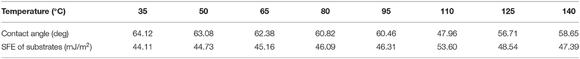
Table 1. Contact angle and corresponding SFEs of substrates heated to different temperatures.
Materials Characterization and Analyses
To evaluate the results of the novel exfoliation process, material characterization was necessary. First, we observed the characteristic peaks of three MoS2 nanoflakes in a photoluminescence spectrum, as shown in Figure 7. We found that the peaks of two test areas were both 631 nm, which is close to the report of Splendiani et al. (2010). In addition, Raman spectra were used to confirm the thickness of the MoS2 flakes with respect to optical principle. Figure 8 shows the Raman spectrum of the sample excited by 532 nm laser line at room temperature. Both and A1g peaks in the spectrum were observed in three flakes. Overall, the differences in the two peaks were ~24.6 cm−1 at the test points. Thus, consulting Liang and Meunier (2014), we can confirm that all of the flakes were multilayered. Subsequently, the above analyses were further verified via AFM through a microimage of two MoS2 nanoflakes exfoliated after thermal treatment of the substrate, from which it was verified that the thicknesses of the flakes were 4.6 and 4.5 nm, respectively, as shown in Figure 9. Because the thickness of an MoS2 atomic layer is 0.65 nm, these flakes are about seven atomic layers thick. This is consistent with the features of multilayers, as confirmed by the Raman spectra (Liang and Meunier, 2014).
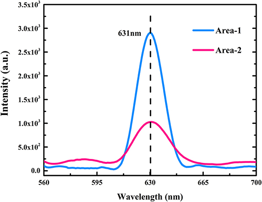
Figure 7. Photoluminescence spectrum of two test areas.
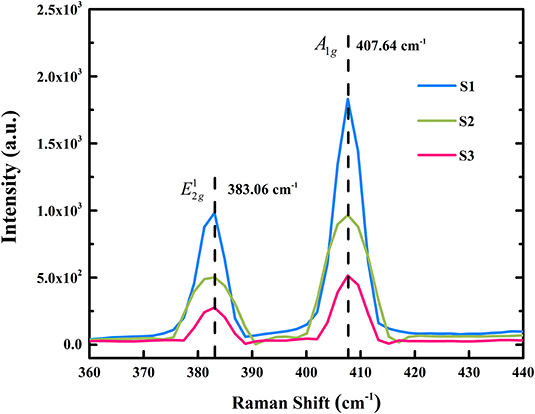
Figure 8. Raman spectrum of three MoS2 samples exfoliated using the new process.
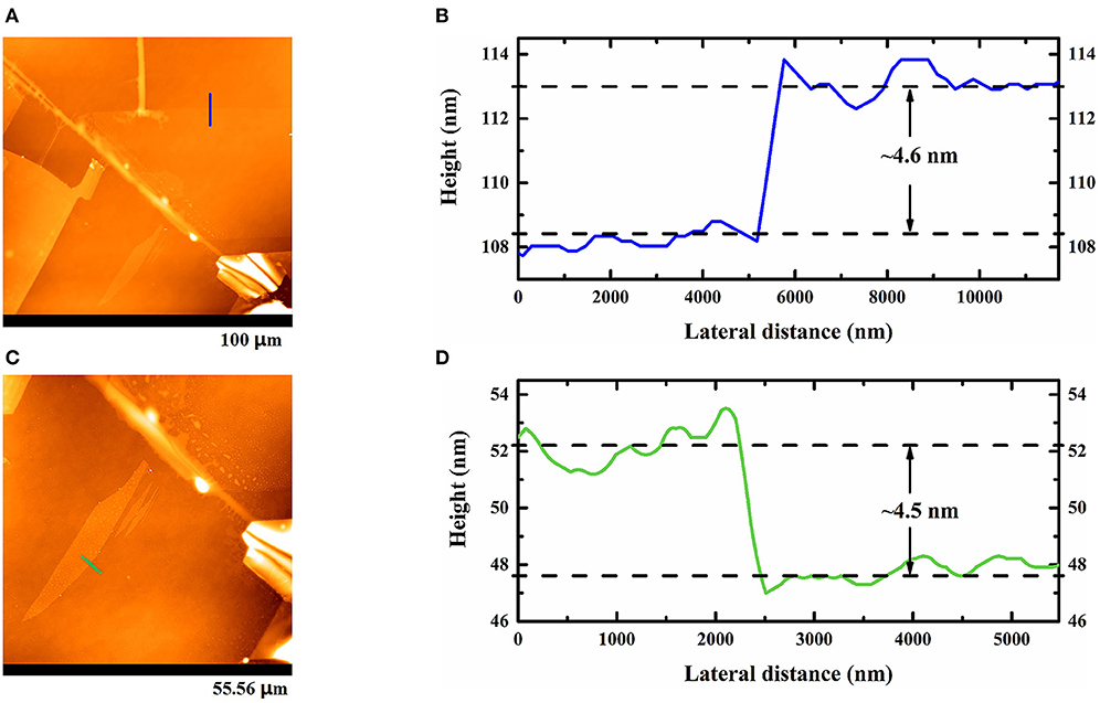
Figure 9. AFM images of three multilayer MoS2 nanoflakes (A,C) achieved with pre-heating and their corresponding height profiles, as shown in (B,D).
Device Performance
The characterization and discussion indicate that semiconducting devices can be produced more easily with the new process of thermal treatment outlined here, due to the high yield and big size of the MoS2 nanoflakes. Using an MoS2 nanoflake prepared by substrate heating, an FET was fabricated to assess the applicative effects of new processes. The device was built according to the so-called bottom-gate and top-contact structure, using Ag as a drain-source electrode and n-type-doped Si as a gate electrode. A structural sketch and a micro-image for FET are shown in Figures 10A,B, respectively. The output and transfer curves of the device are exhibited in Figures 10C,D, allowing us to ascertain that the saturated current in the channel is 1.28 × 10³ μA (VG = 10 V). When VDS = 10 V, the on/off ratio of IDS in this device is ~105, and the subthreshold swing is 317.46 mV/dec. Furthermore, due to the negative threshold voltage extracted from transfer curve, we can confirm that this device belongs to the depletion type. Additionally, the field-effect mobility of the device is 24.26 cm2/Vs, which is extracted with Equation 3, where μsat is the field-effect mobility in the saturated region of the device, L and W are the length and width of device channel, IDS is the channel current of FET, VG is the bias voltage between the gate and source electrode, and Ci is the typical capacitor value of SiO2 in the unit area as 11.5 nf/cm2. The electronic properties of the device were generally consistent with those found in an earlier work (Zhang et al., 2020), as shown in Table 2.
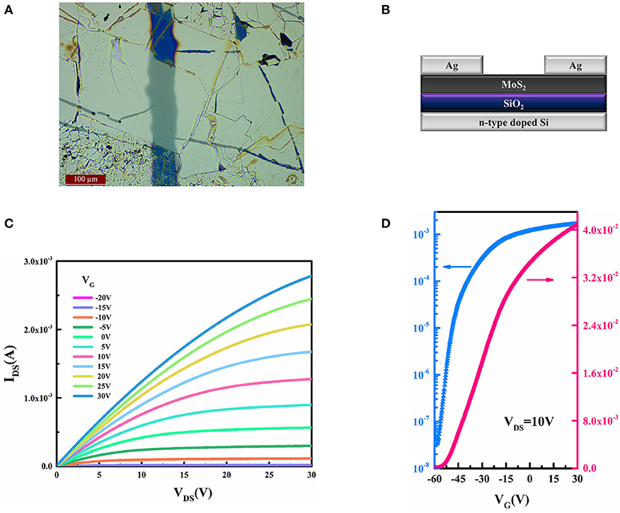
Figure 10. (A) Structure and (B) microimage of MoS2-FET and its (C) output curve and (D) transfer curve.
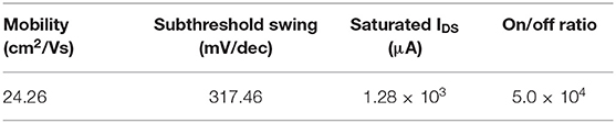
Table 2. Performance of MoS2-FET using the new exfoliation process.
Conclusion
We here report a simple way of improving the yield and size of MoS2 nanoflake preparation. Specifically, we exfoliate the samples with precooling after heating at 110°C for 5 h. The statistics on the microimages indicate that the quality of the flakes is obviously improved, which can be attributed to the differences in the van Der Waals force and the increase in SFE at the interface induced by thermal treatment. Using Raman and photoluminescence spectra, the multilayered structures of the MoS2 crystals are clarified. Following the new exfoliation process, an MoS2-FET was fabricated with an on/off current ratio of ~105, a field-effect mobility of 24.26 cm2/Vs when VDS = 10 V, and a saturated current of 1.28 × 10³ μA when VG = 10 V, values that are generally consistent with those of devices reported previously. These results indicate that the method developed in this paper can efficiently prepare MoS2-FET and has a significant opportunity to become standard procedure for the preparation of 2D materials with an atomic layer structure.
Data Availability Statement
The original contributions presented in the study are included in the article/supplementary material, further inquiries can be directed to the corresponding author/s.
Author Contributions
YZ and XC: writing. SH, GZ, MZ, WQ, ZW, and XH: perform experiment. JW and HZ: supervision and review. All authors contributed to the article and approved the submitted version.
Funding
This work was supported by the Natural Science Foundation of Fujian Province, China (2017J01733, 2018J01641, and 2019J01880), Scientific research guidance project (2017H0004) funded by the Fujian Provincial Department of Science, Fund of Fujian Innovation Center of Additive Manufacturing (ZCZZ202-23), and National Fund Cultivation Project of Fujian Jiangxia University (JXZ2020002 and JXZ2020005).
Conflict of Interest
The authors declare that the research was conducted in the absence of any commercial or financial relationships that could be construed as a potential conflict of interest.
References
Beal, A. R., Knights, J. C., and Liang, W. Y. (1972). Transmission spectra of some transition metal dichalcogenides. II. Group VIA: trigonal prismatic coordination. J. Phys. C: Solid State Phys. 5:3540. doi: 10.1088/0022-3719/5/24/016
Cartz, L., Srinivasa, S. R., Riedner, R. J., Jorgensen, J. D., Worlton, T. G., et al. (1979). Effect of pressure on bonding in black phosphorus. J. Chem. Phys. 71, 1718–1721. doi: 10.1063/1.438523
Desai, S. B., Madhvapathy, S. R., Amani, M., Kiriya, D., Hettick, M., Tosun, M., et al. (2016). Gold-mediated exfoliation of ultralarge optoelectronically-perfect monolayers. Adv. Mater. 28, 4053–4058. doi: 10.1002/adma.201506171
Dines, M. (1975). Lithium intercalation via n-butyllithium of the layered transition metal dichalcogenides. Mater. Res. Bull. 10, 287–291. doi: 10.1016/0025-5408(75)90115-4
Dong, Y. Y., Wang, Y., and Zhang, F. Y. (2010). Inorganic and Analytical Chemistry. Beijing: Science Press.
Huang, X., Zeng, Z. Y., and Zhang, H. (2013). Metal dichalcogenide nanosheets: preparation, properties and applications. Chem. Soc. Rev. 42, 1934–1946. doi: 10.1039/c2cs35387c
Huang, Y., Pan, Y. H., Yang, R., Bao, L. H., Meng, L., Luo, H. L., et al. (2020). Universal mechanical exfoliation of large-area 2D crystals. Nat. Commun. 11:2453. doi: 10.1038/s41467-020-16733-4
Jin, Z., Shin, S., Kwon, D., Han, S. J., and Min, Y. S. (2014). Novel chemical route for atomic layer deposition of MoS2 thin film on SiO2/Si substrate. Nanoscale 6, 14453–14458. doi: 10.1039/C4NR04816D
Joensen, P., Frindt, R., and Morrison, S. (1986). Single-layer MoS2. Mater. Res. Bull. 21, 457–461. doi: 10.1016/0025-5408(86)90011-5
Kim, S., Konar, A., Hwang, W., Lee, J. K., Lee, J., Yang, J., et al. (2012). High-mobility and low-power thin-film transistors based on multilayer MoS2 crystals. Nat. Commun. 3:1011. doi: 10.1038/ncomms2018
Kwon, H., Jang, J., Kim, S., Subramanian, V., and Grigoropoulos, C. P. (2014). Electrical characteristics of multilayer MoS2 transistors at real operating temperatures with different ambient conditions. Appl. Phys. Lett. 105:152105. doi: 10.1063/1.4898584
Kwon, H. J., Kang, H., Jang, J., Kim, S., and Grigoropoulos, C. P. (2014). Analysis of flicker noise in two-dimensional multilayer MoS2 transistors. Appl. Phys. Lett. 104:083110. doi: 10.1063/1.4866785
Li, D., and Neumann, A. (1990). A reformulation of the equation of state for interfacial tensions. J. Colloid Interface Sci. 137, 304–307. doi: 10.1016/0021-9797(90)90067-X
Li, H., Wu, J., Yin, Z., and Zhang, H. (2014). Preparation and applications of mechanically exfoliated single- and multi-layer MoS2 and WSe2 nanosheets. Acc. Chem. Res. 47, 1067–1075. doi: 10.1021/ar4002312
Liang, L., and Meunier, V. (2014). First-principles raman spectra of MoS2, WS2 and their heterostructures. Nanoscale 6, 5394–5401. doi: 10.1039/c3nr06906k
Lin, Y., Williams, T. V., and Connell, J. W. (2010). Soluble, exfoliated hexagonal boron nitride nanosheets. J. Phys. Chem. Lett. 1, 277–283. doi: 10.1021/jz9002108
Liu, K. K., Zhang, W., Lee, Y. H., Lin, Y. C., Chang, M. T., Su, C. Y., et al. (2005). Growth of large-area and highly crystalline MoS2 thin layers on insulating substrates. Nano Lett. 12, 1538–1544. doi: 10.1021/nl2043612
Lv, R., Robinson, J. A., Schaak, R. E., Sun, D., Sun, Y., Mallouk, T. E., et al. (2015). Transition metal dichalcogenides and beyond: synthesis, properties, and applications of single- and few-layer nanosheets. Acc. Chem. Res. 48, 56–64. doi: 10.1021/ar5002846
Mak, K. F., He, K., Shan, J., and Heinz, T. F. (2012). Control of valley polarization in monolayer MoS2 by optical helicity. Nat. Nanotechnol. 7, 494–498. doi: 10.1038/nnano.2012.96
Nicolosi, V., Chhowalla, M., Kanatzidis, M., Strano, M. S., and Coleman, J. N. (2013). Liquid exfoliation of layered materials. Science 340:1226419. doi: 10.1126/science.1226419
Niu, L., Coleman, J. N., Zhang, H., Shin, H., Chhowalla, M., and Zheng, Z. (2016). Production of two-dimensional nanomaterials via liquid based direct exfoliation. Small 12, 272–293. doi: 10.1002/smll.201502207
Novoselov, K. S., Geim, A. K., Morozov, S. V., Jiang, D., Zhang, Y., Dubonos, S. V., et al. (2004). Electric field effect in atomically thin carbon films. Science 306, 666–669. doi: 10.1126/science.1102896
Ong, W. J., Tan, L. L., Ng, Y. H., Yong, S. T., and Chai, S. P. (2016). Graphitic carbon nitride (g-C3N4)-based photocatalysts for artificial photosynthesis and environmental remediation: are we a step closer to achieving sustainability. Chem. Rev. 116, 7159–7329. doi: 10.1021/acs.chemrev.6b00075
Qiu, H., Pan, L., Yao, Z., Li, J., Shi, Y., and Wang, X. (2012). Electrical characterization of back-gated bi-layer MoS2 field-effect transistors and the effect of ambient on their performances. Appl. Phys. Lett. 100:123104. doi: 10.1063/1.3696045
Radisavljevic, B., Radenovic, A., Brivio, J., Giacometti, V., and Kis, A. (2011). Single-layer MoS2 transistors. Nat. Nanotechnol. 6, 147–150. doi: 10.1038/nnano.2010.279
Riikka, L. (2005). Surface chemistry of atomic layer deposition: a case study for the trimethylaluminum/water process. J. Appl. Phys. 97:121301. doi: 10.1063/1.1940727
Splendiani, A., Sun, L., Zhang, Y., Li, T., Kim, J., Chim, C. Y., et al. (2010). Emerging photoluminescence in monolayer MoS2. Nano Lett. 10, 1271–1275. doi: 10.1021/nl903868w
Tan, C. L., and Zhang, H. (2015). Two-dimensional transition metal dichalcogenide nanosheet-based composites. Chem. Soc. Rev. 44, 2713–2731. doi: 10.1039/C4CS00182F
Weng, Q., Wang, X., Wang, X., Bando, Y., and Golberg, D. (2016). Functionalized hexagonal boron nitride nanomaterials: emerging properties and applications. Chem. Soc. Rev. 45, 3989–4012. doi: 10.1039/C5CS00869G
Wilson, J. A., and Yoffe, A. D. (1969). The transition metal dichalcogenides discussion and interpretation of the observed optical, electrical and structural properties. Adv. Phys. 18, 193–335. doi: 10.1080/00018736900101307
Wu, S., Huang, C., Aivazian, G., Ross, J. S., Cobden, D. H., and Xu, X. (2013). Vapor-solid growth of high optical quality MoS2 monolayers with near-unity valley polarization. ACS Nano 7, 2768–2772. doi: 10.1021/nn4002038
Yi, M., and Shen, Z. A. (2015). A review on mechanical exfoliation for the scalable production of graphene. J. Mater. Chem. A 3, 11700–11715. doi: 10.1039/C5TA00252D
Zhang, H. (2015). Ultrathin two-dimensional nanomaterials. ACS Nano 9, 9451–9469. doi: 10.1021/acsnano.5b05040
Zhang, J., Chen, Y., and Wang, X. (2015). Two-dimensional covalent carbon nitride nanosheets: Synthesis, functionalization, and applications. Energy Environ. Sci. 8, 3092–3108. doi: 10.1039/C5EE01895A
Zhang, X., Xie, H., Liu, Z., Tan, C., Luo, Z., Li, H., et al. (2015). Black phosphorus quantum dots. Angew. Chem. Int. Ed. 54, 3653–3657. doi: 10.1002/anie.201409400
Keywords: MoS2, exfoliation, thermal treatment, surface free energy, van de Waals force, FET
Citation: Zhang Y, Chen X, Zhang H, Hu S, Zhao G, Zhang M, Qin W, Wang Z, Huang X and Wang J (2021) Facile Exfoliation for High-Quality Molybdenum Disulfide Nanoflakes and Relevant Field-Effect Transistors Developed With Thermal Treatment. Front. Chem. 9:650901. doi: 10.3389/fchem.2021.650901
Received: 08 January 2021; Accepted: 09 March 2021;
Published: 26 April 2021.
Edited by:
Andreas Rosenkranz, University of Chile, ChileReviewed by:
Lei Chen, Southwest Jiaotong University, ChinaDer-Yuh Lin, National Changhua University of Education, Taiwan
Kunhong Hu, Hefei University, China
Copyright © 2021 Zhang, Chen, Zhang, Hu, Zhao, Zhang, Qin, Wang, Huang and Wang. This is an open-access article distributed under the terms of the Creative Commons Attribution License (CC BY). The use, distribution or reproduction in other forums is permitted, provided the original author(s) and the copyright owner(s) are credited and that the original publication in this journal is cited, in accordance with accepted academic practice. No use, distribution or reproduction is permitted which does not comply with these terms.
*Correspondence: Hao Zhang, emhhbmdoQGZqanh1LmVkdS5jbg==; Jun Wang, d2FuZ2pAc2l0LmVkdS5jbg==