 Jinming Wu1
 Shuang Yang
 Wei Zhu
- 1State Key Laboratory of Crystal Materials, Institute of Crystal Materials, Shandong University, Jinan, China
- 2Institute of Radiation Medicine, Shandong Academy of Medical Sciences, Shandong First Medical University, Jinan, China
- 3Sunzhou Research Institute, Shandong University, Suzhou, China
- 4LinYi Ecological Environmental Bureau, LinYi, China
Metal halide perovskite single-crystal detectors have attracted increasing attention due to the advantages of low noise, high sensitivity, and fast response. However, the narrow photoresponse range of widely investigated lead-based perovskite single crystals limit their application in near-infrared (NIR) detection. In this work, tin (Sn) is incorporated into methylammonium lead iodide (MAPbI3) single crystals to extend the absorption range to around 950 nm. Using a space-confined strategy, MAPb0.5Sn0.5I3 single-crystal thin films with a thickness of 15 μm is obtained, which is applied for sensitive NIR detection. The as-fabricated detectors show a responsivity of 0.514 A/W and a specific detectivity of 1.4974×10¹¹ cmHz1/2/W under 905 nm light illumination and –1V. Moreover, the NIR detectors exhibit good operational stability (∼30000 s), which can be attributed to the low trap density and good stability of perovskite single crystals. This work demonstrates an effective way for sensitive NIR detection.
Introduction
Metal halide perovskite with an ABX3 structure shows promising potential for various applications, such as detectors and solar cells (Xiao et al., 2014), light-emitting diodes, lasers, and field-effect transistors, due to long carrier diffusion length, tunable optical bandgaps, flexibility, low cost and easy fabrication (Ju et al., 2019). Recently, the power conversion efficiency of perovskite solar cells has reached 25.5% (Best Research-Cell Effici, 2021), which sets a new efficiency benchmark for solution-processed solar cells. Perovskite photodetectors also show excellent performances such as fast response speed, high detectivity, low noise, and large linear dynamic range (Li et al., 2020).
Up to now, the most widely studied perovskite detectors are based on polycrystalline films, which included grain boundary, small grain sizes, and pinhole and low surface coverage (Wang and Kim, 2017; Yang et al., 2017; Li et al., 2019; Zhao et al., 2020). A slow crystallization process is believed to provide a universal strategy to improve crystal quality (Liu et al., 2018). Compared to polycrystalline thin films, higher crystallization quality and longer carrier diffusion length can be observed in single crystals (Huang et al., 2015; Liu et al., 2016). Additionally, the remarkable stability of single crystals could enhance the stability of optoelectronic devices (Zhang Y et al., 2018). For example, Bao et al. (2017) reported visible-light photodetectors based on MAPbI3 (iodine) and MAPbBr3 (bromine) single-crystal thin film with high photoresponsivity, low noise, and large linear dynamic range. Chen et al. (2019a) fabricated visible-blind UV (ultraviolet) photodetectors based on MAPbCl3 (chlorine) single-crystal thin film with 15-ns response time.
It should be noted that perovskite single crystals based on Pb show a typical optical bandgap (Eg) > 1.5 eV, which limits the capture of photons in the NIR region. To obtain sufficient optical absorption in the NIR region, a new component and other sensitizers can be introduced into Pb (lead)-based perovskite. Among all the alternative elements for the toxic Pb element, Sn is a promising candidate for the extension of the absorption range. Zhu et al. (2018) reported photodetectors based on Sn–Pb mixed polycrystalline thin films with A-cation engineering, which achieved larger photocurrent and lower noise current between 340 and 1000 nm. You et al. reported stable Pb–Sn mixed low-bandgap perovskite solar cells with composition engineering (Chi et al., 2018). By adjusting the ratio of Pb2+ and Sn2+, the absorption range of mixed Pb–Sn perovskite can be extended into the NIR region, which is an effective and green strategy to achieve NIR response. Therefore, it is important for developing Pb–Sn mixed single-crystal thin films as a light absorption layer for NIR detectors.
In this work, MAPb0.5Sn0.5I3 single-crystal thin films with a thickness of 15 μm and high crystallization quality are grown by using the space-confined method. Partial substitution of Pb in MAPbI3 with Sn can reduce toxicity and lower the bandgap. The employment of MAPb0.5Sn0.5I3 single-crystal thin films in NIR detectors has been demonstrated with high detectivity and operational stability, which provides a less-toxic alternative material for sensitive NIR detection.
Materials and Methods
Materials
Chemicals and reagents: Methylcholine iodide (MAI) was synthesized from stannic iodide produced by Xi’an Polymer Light Technology. Gamma-butyrolactone (GBL, 99%) was purchased from Aladdin Reagent Ltd. Fullerene (C60), 2,9-dimethyl-4,7-diphenyl-1,10-phenathroline (BCP), and polytriaryl amine (PTAA) were purchased for Xi’an Polymer Light Technology.
Preparation of MAPb0.5Sn0.5I3 single-crystal thin film: indium tin oxide (ITO) substrates were washed in deionized water about 15 min by an ultrasonic cleaner (KS-3200E), then a surface treatment by ultraviolet–ozone (UVO) for 10 min was carried out. Next, the hydrophobic and conductive films were fabricated by a spin coating PTAA solution (0.2 wt% in chlorobenzene) at 3,000 rpms, and subsequently annealed at 100°C for 15 min.
The single-crystal thin film was grown by using the space-confined method with a hydrophobic interface. A drop of the prepared 1.7M MAPb0.5Sn0.5I3 precursor solution in GBL was inserted into two ITO covered by PTAA substrates. Then, substrates were placed on a hot plate with a temperature of 45°C for 10 min. Subsequently, the temperature was raised to 95°C to further promote the nucleation and growth of single-crystal thin films. Finally, the two substrates were carefully separated to get the single-crystal thin film on substrates with a blade.
Infrared Detector Device Fabrication:C60 (40 nm) and BCP (3 nm) were thermally evaporated at a rate of 0.2 Å/s to form the charge transport layer. Cu (80 nm) was thermally evaporated at a rate of 0.8 Å/s to form the electrode. Au (40 nm) was thermally evaporated at a rate of 0.6 Å/s to form the electrode.
Characterizations
X-Ray Diffraction
Powder X-ray diffraction (PXRD) patterns were measured on a smartLab SE High Resolution Diffraction System with Cu Kα1 radiation (λ = 1.54186Å) in the range of 5–90°(2θ) with a single-crystal thin film of 2 × 1 × 0.02 mm3 in size.
Scanning Electron Microscope
The surface and cross-morphologies images were taken from a field emission (Phenom Pharos).
Steady-state absorption: Absorption spectra were determined using a U3500 Hitachi UV/Vis Spectrophotometer with the self-made mold of test.
Energy-Dispersive Spectrometer
The element components with a single-crystal thin film of 2 × 1 × 0.02 mm3 in size were measured by using a desktop field-emission scanning electron microscope energy spectrum all-in-one machine (Phenom Pharos).
Thermogravimetric Analysis and Differential Scanning Calorimetry Measurements
TGA and DSC curves were characterized by using a TGA/DSC analyzer (Setaram). The powder, which was collected using by a single-crystal thin film, was placed in an aluminum crucible and heated at a rate of 10 K/min from room temperature to 800°C under flowing nitrogen gas.
Device Characterizations
Device I-V characteristics were collected by using a Keithley 2400 analyzer. AM 1.5-G irradiation (100 mW/cm2) was produced by a xenon lamp-based solar simulator. NIR laser of 10 mW intensity was provided by the NIR light source (ZLM50AX905-16GD). A tunable power was carried out by the adjustment of Cu film thickness. Pinc = P/A, where A is the active area of the light spot, Pinc is the incident power density, and P is the incident power.
Results and Discussion
The inverse temperature crystallization (ITC) method was applied for the growth of MAPb0.5Sn0.5I3 single crystals in which solubility decreases with increasing temperature (Saidaminov et al., 2015). To grow micrometer-thick single-crystal thin films, the precursor solution was inserted into two ITO substrates, and the crystal thickness was determined by the substrate gap (Figure 1).
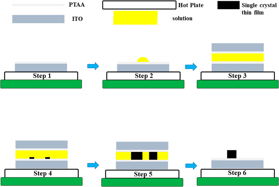
FIGURE 1. Schematic illustration of single-crystal thin film growth process by using the space-confined method.
Figure 2A shows the photographs of as-grown MAPb0.5Sn0.5I3 single-crystal thin films with a thickness of 15 μm. The crystal shape is hexagonal, which is similar to that of MAPbI3 single-crystal thin films. SEM is employed to study the surface thickness and morphology. It can be seen from the cross-sectional SEM image (Figure 2B) that the thickness of the single-crystal thin film is about 15 µm. The top-view SEM image (Figure 2C) indicates the absence of grain boundaries for a single-crystal thin film and the surface is very smooth.
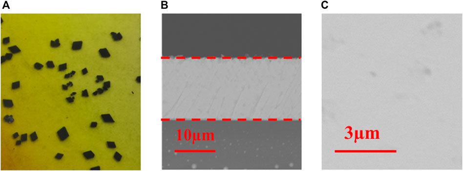
FIGURE 2. (A) Photograph, (B) cross-sectional SEM images, and (C) surface morphology SEM images of a MAPb0.5Sn0.5I3 single-crystal thin film.
In Figure 3A, the XRD patterns of MAPb0.5Sn0.5I3 single-crystal thin films mainly show two diffraction peaks at 20.03º and 40.51º, which can be assigned to (110) and (220) planes, indicating that the MAPb0.5Sn0.5I3 single-crystal thin films are grown along the [110] orientation. Furthermore, it can be noted that the XRD patterns of the MAPb0.5Sn0.5I3 single-crystal thin film show negligible change after storage in air and N2 atmosphere for 10 days, implying its good structure stability. As shown in Figure 3B, the absorption onset peak is 950 nm for MAPb0.5Sn0.5I3 single-crystal thin film, which corresponds to a suitable small bandgap of 1.3 eV. The conjunction of a glass substrate and ITO electrodes exhibits a fully transparent device for the incident light direction. To examine the thermal stability of MAPb0.5Sn0.5I3 single crystal thin film from the substrates and then measured by TGA and DSC (Figures 3C,D). The TGA curve of MAPb0.5Sn0.5I3 exhibits obvious mass loss after 170°C and comprises three-step decomposition process, including the evaporation of MAI, SnI2, and PbI2. In the DSC curve, a clear exothermal peak is shown at 350°C, corresponding to the melting point of MAPb0.5Sn0.5I3.
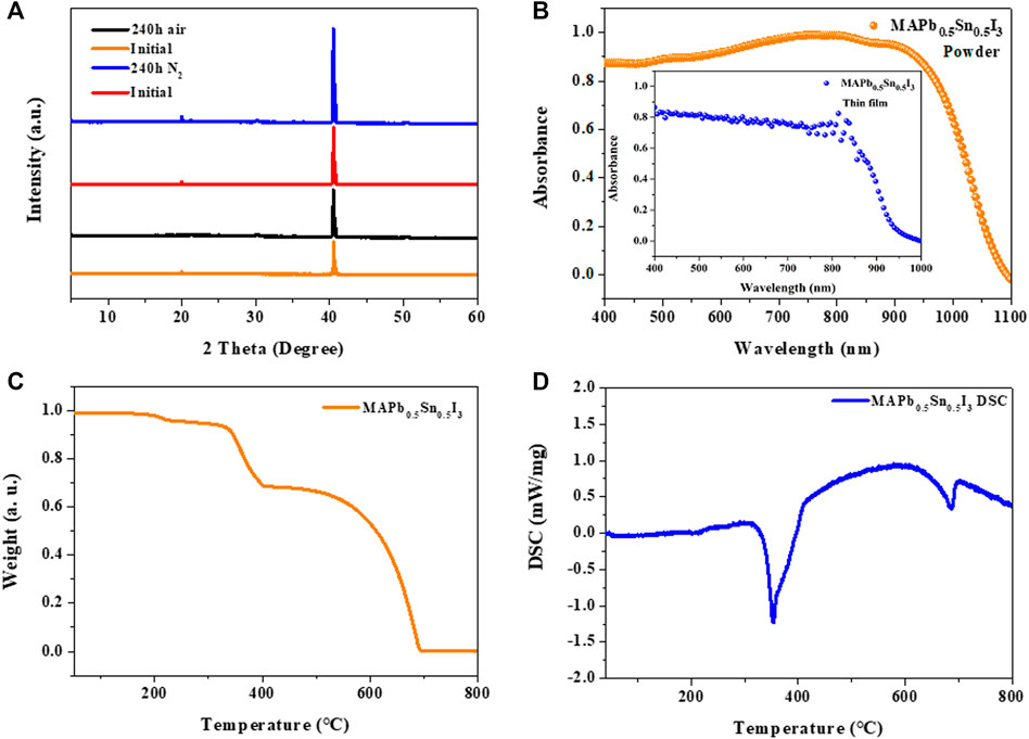
FIGURE 3. (A) XRD pattern of a MAPb0.5Sn0.5I3 single-crystal thin film. (B) UV-Vis-NIR absorption normalized spectra of thin film and UV-Vis diffuse reflectance of powder. (C) TGA and (D) DSC data for MAPb0.5Sn0.5I3.
EDS measurement is adopted to analyze the chemical composition of the as-grown single-crystal thin films. According to Table 1 and Figure 4, we can verify that single-crystal thin films with Pb/Sn ratio of nearly 1:1 are synthesized by combining the ITC and space-confined methods. The aforementioned results confirm successful preparation of MAPb0.5Sn0.5I3 single-crystal thin films with good structure stability and absorption extended into the NIR region.

TABLE 1. SEM–EDS results of element components and ratio of a MAPb0.5Sn0.5I3 single-crystal thin film.
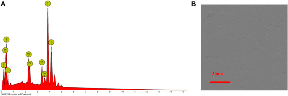
FIGURE 4. (A) Energy-dispersive X-ray spectroscopy of MAPb0.5Sn0.5I3 in (B) surface zone.
Superior optoelectronic properties are required for high-performance photodetectors. To characterize the hole mobility and hole trap density of as-grown MAPb0.5Sn0.5I3 single-crystal thin films, hole-only devices with the structure of ITO/PTAA/single crystals/Au were fabricated, as is shown in Figure 5A. The hole mobility and trap density are calculated according to the following two equations:
where ε is the relative dielectric constant, ε0 is the dielectric constant of free space, d is the film thickness, V is the bias, and µ is carrier mobility;
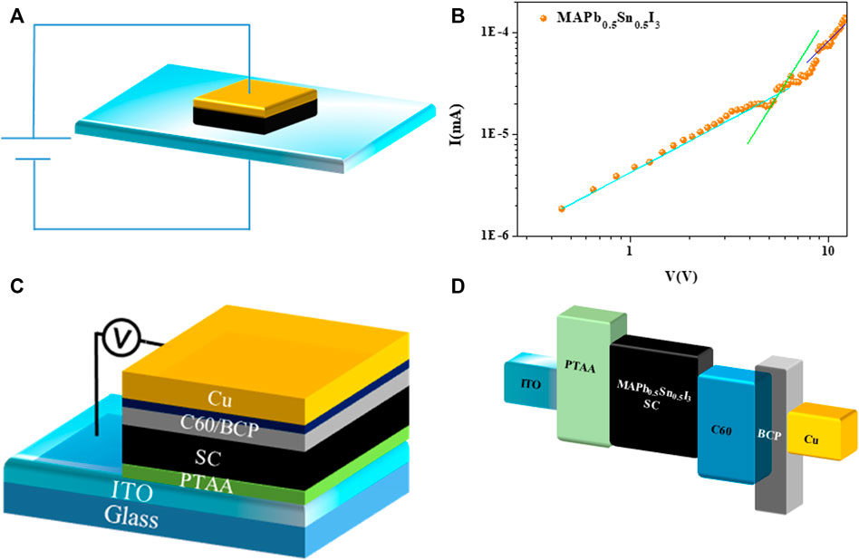
FIGURE 5. (A) Schematic device structure. (B) Dark current–voltage curves of hole-only devices based on a MAPb0.5Sn0.5I3 single-crystal thin film. (C) Schematic device structure and (D) energy band diagram of MAPb0.5Sn0.5I3.
where VTFL is the voltage at which all the traps are filled, e is the elementary charge, and nt is the hole trap density (Zhang Y et al., 2018; Kim et al., 2021). The hole mobility and trap density are calculated to be 0.001485 cm2V−1s−1 and 6.948×1013 cm−3 (Figure 5B), respectively. In contrast to the pure lead-based perovskite single crystals, the mobility is relatively low, while the trap density is relatively high, which should be due to the oxidation of Sn2+ to Sn4+. Future optimization can be focused on how to avoid the oxidation of Sn2+, such as introduction of reductants, which is under investigation in our laboratory.
To explore the application of MAPb0.5Sn0.5I3 single-crystal thin films in NIR detection, photodetectors were easily fabricated by depositing the electron transport layer and metal electrode, benefiting the substrate/hole transport layer (HTL)–integrated growth of single-crystal films (Chen et al., 2019b). As shown in Figure 5C, the device structure of ITO/PTAA/MAPb0.5Sn0.5I3 single-crystal thin film/C60/bathocuproine (BCP)/copper (Cu). The hydrophobic PTAA layer functions as both the hole transporting layer and non-wetting interface, which is beneficial for the improvement of crystallization and fabrication of the device (Bi et al., 2015). The BCP layer can enhance the surface smoothness of C60 and reduce the trapped electrons (Kavadiya et al., 2020; Ying et al., 2021). The energy diagram of the detector is shown in Figure 5D, exhibiting that the PTAA hole transport layer and C60/BCP electron transport layer can promote the charge extraction at zero bias (Meng et al., 2016).
Effective carrier collection plays a significant role in responsivity of the detectors, which is evaluated by the external quantum efficiency (EQE) measurement under zero bias (Fang et al., 2015). The EQE is defined as the ratio between the number of photogenerated carriers and incident photons at a certain wavelength, which can be applied for evaluating the photoelectric conversion ability of photodetectors (Dong Q et al., 2015; Liu et al., 2019). As shown in Figure 6A, EQE values of 3% for MAPb0.5Sn0.5I3 single-crystal detectors at 905 nm are obtained under zero bias. The EQE values are consistent with the relative low mobility of MAPb0.5Sn0.5I3 single-crystal films.
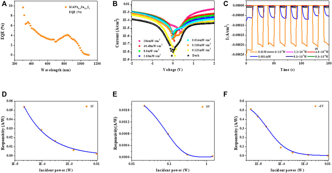
FIGURE 6. (A) EQE curves of MAPb0.5Sn0.5I3 single-crystal devices under zero bias. (B) Current–voltage curves of a MAPb0.5Sn0.5I3 single-crystal devices under 905 nm near-infrared light illumination and dark. A single-crystal thin film device based on MAPb0.5Sn0.5I3 response to 905 nm near-infrared light by turning the source on and off (C) at zero bias. Relationship between the photocurrent and the incident light intensity at 1V (D), 0V (E), and –1V (F).
To directly display the performance of NIR detectors, current density–voltage (J-V) measurements were carried out in the dark and illuminated with 905 nm light (Figure 6B). When the light intensity increases from 0.13 mW/cm2 to 284 mW/cm2, the photovoltage increases from 0.09 to 0.36 V. The existence of a photovoltage indicates the NIR photodetectors can work without external bias. Therefore, we mainly focus on the device performance under zero bias, which is so-called self-powered photodetectors. The responsivity (R) and detectivity (D*) are key parameters for evaluating the performances of photodetectors (Liu et al., 2018), which can be calculated according to the following equations:
where Iphoto and Plight are the photocurrent and incident optical power, A is the area of device, q is the charge value of an electron, and Idark are the dark currents. In the time-dependent photocurrent curve, it can be noted that the on/off ratio was about 103, at 284 mWcm−2 incident light intensity, demonstrating an obvious response for 905 nm at 0V bias (Figure 6B). When the incident light intensity was adjusted to 40.48 mWcm−2, the response current is strikingly measured to reduce from 2 × 10⁻⁵ Acm−2 to 1.5 × 10⁻⁶ Acm−2, for which the comparison can be attributed to the defects (Figures 6B,C). But the response current still shows the obvious difference until 4.65 × 10⁻⁶W (0.13161 mWcm−2) at an applied bias of 0V (Figure 6C). With all the aforementioned measurement device performances, we demonstrated a promising NIR detector at zero bias with the employment of MAPb0.5Sn0.5I3 single-crystal thin films. We further measured the detector performance by using a quantitative analysis for the device under zero bias and –1V and 1V, respectively. We further investigated the relationship between the responsivity and light intensity. Figures 6D–F exhibits the light density–dependent responsivity, and the result proves our MAPb0.5Sn0.5I3 based on the NIR detector showing apparent intensity-dependent characteristics, and a lower light intensity leads to a larger responsivity. Responsivity as a function of the light intensity is shown in Figure 6D with bias at 1V. The responsivity decreases at high incidence, and this mechanism can attribute to previous reports for electronic trap states at the perovskite–ITO interface (Muñoz et al., 1997; Konstantatos et al., 2006; Lhuillier et al., 2013; Dong R et al., 2015). The NIR photodetector exhibits a responsivity of 0.0539 A/W and a detectivity of 1.86×10¹⁰ cmHz1/2W−1 at 1 V bias. Under 0.6143 mWcm−2 incident light intensity of 905 nm, the highest R and D* are calculated to be 0.01746 A/W and 3.08×10¹⁰ cmHz1/2W−1 at zero bias (Figure 6E), respectively. In addition, at low power (4.65 × 10⁻⁶ W), responsivity is measured to be 0.514 A/W at –1V bias (Figure 6F). Based on the combination of information in the dark and the responsivity, we could calculate the detectivity about 1.497×10¹¹ cmHz1/2W−1 at –1V bias.
Finally, we further investigated the operational stability for the single-crystal thin films based on the NIR detector. The lifetime of detector is mainly determined by the operational stability (Lei et al., 2018; Wu et al., 2021). As shown in the Figure 7A, the device maintained average 70% operational performance, irradiated by 905 nm NIR light source with 284 mW/cm2 after continuous 30000 s in N2 atmosphere. Figure 7B shows that the detector showed a stable response current up to 4000 s at zero bias.
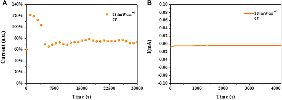
FIGURE 7. (A) Operational stability of a MAPb0.5Sn0.5I3 single-crystal device under 284 mW/cm2 905 nm near-infrared light with continuous illumination at zero bias. (B) Response current stability of device based on a MAPb0.5Sn0.5I3 single crystal under 284 mW/cm2.
Discussion
The oxidation of Sn2+ increased the deep traps for an obvious decrease in the photocurrent, which becomes a critical factor for the carrier transport (Cheng et al., 2020). The photocurrent declines distinctly when decreasing the light intensity, which was originated from capture of deep traps of the surface for carriers. The photogenerated carriers were captured by the main deep traps from the surface, and the interface of poor contact, [34] as a result, photocurrent exhibited the reduction in an order of magnitude or more.
Conclusion
In summary, in this work, we demonstrate the first efficient NIR detector with MAPb0.5Sn0.5I3 single-crystal thin films grown by using the space-confined method. The mixed Pb–Sn element can enable a wider response range for NIR detection. In addition, the single-crystal thin films with reduced Pb contents exhibit less toxicity, and the partial existence of Pb can avoid severe oxidation of Sn2+ in pure Sn-based perovskites, leading to an enhanced operational stability of detectors. Notably, the MAPb0.5Sn0.5I3-based NIR detector shows obvious photoresponse at zero bias and a responsivity of 0.0016 A/W as well as a detectivity of 3.08×10¹⁰ cmHz1/2/W. We believe that the incorporation of Sn in Pb-based perovskite single-crystal thin films will provide an alternative route for achieving efficient NIR detectors.
Data Availability Statement
The original contributions presented in the study are included in the article/supplementary material; further inquiries can be directed to the corresponding authors.
Author Contributions
ZC, WZ, and SY devised the project. JW synthesized the single crystals and conducted all the characterization. YZ provided the detailed guidance. All authors contributed to manuscript revision, read, and approved the submitted version.
Funding
This work was economically supported by the National Natural Science Foundation of China (Grant No. 52002221), Natural Science Foundation of Jiangsu Province (BK20200230, BK20190206), and Natural Science Foundation of Shandong Province (ZR2020QE059).
Conflict of Interest
The authors declare that the research was conducted in the absence of any commercial or financial relationships that could be construed as a potential conflict of interest.
The handling editor declared a past co-authorship with the authors SY and ZC.
Publisher’s Note
All claims expressed in this article are solely those of the authors and do not necessarily represent those of their affiliated organizations, or those of the publisher, the editors, and the reviewers. Any product that may be evaluated in this article, or claim that may be made by its manufacturer, is not guaranteed or endorsed by the publisher.
References
Bao, C., Chen, Z., Fang, Y., Wei, H., Deng, Y., Xiao, X., et al. (2017). Low‐Noise and Large‐Linear‐Dynamic‐Range Photodetectors Based on Hybrid‐Perovskite Thin‐Single‐Crystals. Adv. Mater. 29, 1703209. doi:10.1002/adma.201703209
Best Research-Cell Efficiency Chart. Available at: https://www.nrel.gov/pv/cell-efficiency.html (Accessed on 15 June 2021).
Bi, C., Wang, Q., Shao, Y., Yuan, Y., Xiao, Z., and Huang, J. (2015). Non-wetting Surface-Driven High-Aspect-Ratio Crystalline Grain Growth for Efficient Hybrid Perovskite Solar Cells. Nat. Commun. 6, 7747. doi:10.1038/ncomms8747
Chen, Z., Li, C., Zhumekenov, A. A., Zheng, X., Yang, C., Yang, H., et al. (2019a). Solution‐Processed Visible‐Blind Ultraviolet Photodetectors with Nanosecond Response Time and High Detectivity. Adv. Opt. Mater. 7, 1900506. doi:10.1002/adom.201900506
Chen, Z., Turedi, B., Alsalloum, A. Y., Yang, C., Zheng, X., Gereige, I., et al. (2019b). Single-Crystal MAPbI3 Perovskite Solar Cells Exceeding 21% Power Conversion Efficiency. ACS Energ. Lett. 4, 1258–1259. doi:10.1021/acsenergylett.9b00847.s001
Cheng, X., Yang, S., Cao, B., Tao, X., and Chen, Z. (2020). Single Crystal Perovskite Solar Cells: Development and Perspectives. Adv. Funct. Mater. 30, 1905021. doi:10.1002/adfm.201905021
Chi, D., Huang, S., Zhang, M., Mu, S., Zhao, Y., Chen, Y., et al. (2018). Composition and Interface Engineering for Efficient and Thermally Stable Pb-Sn Mixed Low‐Bandgap Perovskite Solar Cells. Adv. Funct. Mater. 28, 1804603. doi:10.1002/adfm.201804603
Dong, Q., Fang, Y., Shao, Y., Mulligan, P., Qiu, J., Cao, L., et al. (2015). Electron-hole Diffusion Lengths > 175 μm in Solution-Grown CH 3 NH 3 PbI 3 Single Crystals. Science 347, 967–970. doi:10.1126/science.aaa5760
Dong, R., Fang, Y., Chae, J., Dai, J., Xiao, Z., Dong, Q., et al. (2015). High-Gain and Low-Driving-Voltage Photodetectors Based on Organolead Triiodide Perovskites. Adv. Mater. 27, 1912–1918. doi:10.1002/adma.201405116
Fang, Y., Dong, Q., Shao, Y., Yuan, Y., and Huang, J. (2015). Highly Narrowband Perovskite Single-crystal Photodetectors Enabled by Surface-Charge Recombination. Nat. Photon 9, 679–686. doi:10.1038/nphoton.2015.156
Huang, J., Shao, Y., and Dong, Q. (2015). Organometal Trihalide Perovskite Single Crystals: A Next Wave of Materials for 25% Efficiency Photovoltaics and Applications beyond? J. Phys. Chem. Lett. 6, 3218–3227. doi:10.1021/acs.jpclett.5b01419
Ju, D., Zheng, X., Yin, J., Qiu, Z., Türedi, B., Liu, X., et al. (2019). Tellurium-Based Double Perovskites A2TeX6 with Tunable Band Gap and Long Carrier Diffusion Length for Optoelectronic Applications. ACS Energ. Lett. 4, 228–234. doi:10.1021/acsenergylett.8b02113
Kavadiya, S., Onno, A., Boyd, C., Yu, Z., McGehee, M., and Holman, Z. C. (2020). in 2020 47th IEEE Photovoltaic Specialists Conference (PVSC), 1439–1440.
Kim, H., Lee, J. W., Han, G. R., Kim, S. K., and Oh, J. H. (2021). Synergistic Effects of Cation and Anion in an Ionic Imidazolium Tetrafluoroborate Additive for Improving the Efficiency and Stability of Half‐Mixed Pb‐Sn Perovskite Solar Cells. Adv. Funct. Mater. 31, 2008801. doi:10.1002/adfm.202008801
Konstantatos, G., Howard, I., Fischer, A., Hoogland, S., Clifford, J., Klem, E., et al. (2006). Ultrasensitive Solution-Cast Quantum Dot Photodetectors. Nature 442, 180–183. doi:10.1038/nature04855
Lei, L.-Z., Shi, Z.-F., Li, Y., Ma, Z.-Z., Zhang, F., Xu, T.-T., et al. (2018). High-efficiency and Air-Stable Photodetectors Based on lead-free Double Perovskite Cs2AgBiBr6 Thin Films. J. Mater. Chem. C 6, 7982–7988. doi:10.1039/c8tc02305k
Lhuillier, E., Keuleyan, S., Zolotavin, P., and Guyot-Sionnest, P. (2013). Mid-Infrared HgTe/As2S3Field Effect Transistors and Photodetectors. Adv. Mater. 25, 137–141. doi:10.1002/adma.201203012
Li, C., Lu, J., Zhao, Y., Sun, L., Wang, G., Ma, Y., et al. (2019). Highly Sensitive, Fast Response Perovskite Photodetectors Demonstrated in Weak Light Detection Circuit and Visible Light Communication System. Small 15, 1903599. doi:10.1002/smll.201903599
Li, Y., Zhang, Y., Li, T., Tang, X., Li, M., Chen, Z., et al. (2020). A Fast Response, Self-Powered and Room Temperature Near Infrared-Terahertz Photodetector Based on a MAPbI3/PEDOT:PSS Composite. J. Mater. Chem. C 8, 12148–12154. doi:10.1039/d0tc02399j
Liu, S., Wang, L., Lin, W.-C., Sucharitakul, S., Burda, C., and Gao, X. P. A. (2016). Imaging the Long Transport Lengths of Photo-Generated Carriers in Oriented Perovskite Films. Nano Lett. 16, 7925–7929. doi:10.1021/acs.nanolett.6b04235
Liu, Y., Ye, H., Zhang, Y., Zhao, K., Yang, Z., Yuan, Y., et al. (2019). Surface-Tension-Controlled Crystallization for High-Quality 2D Perovskite Single Crystals for Ultrahigh Photodetection. Matter 1, 465–480. doi:10.1016/j.matt.2019.04.002
Liu, Y., Zhang, Y., Yang, Z., Ye, H., Feng, J., Xu, Z., et al. (2018). Multi-inch Single-Crystalline Perovskite Membrane for High-Detectivity Flexible Photosensors. Nat. Commun. 9, 5302. doi:10.1038/s41467-018-07440-2
Meng, L., You, J., Guo, T.-F., and Yang, Y. (2016). Recent Advances in the Inverted Planar Structure of Perovskite Solar Cells. Acc. Chem. Res. 49, 155–165. doi:10.1021/acs.accounts.5b00404
Muñoz, E., Monroy, E., Garrido, J. A., Izpura, I., Sánchez, F. J., Sánchez-Garcı́a, M. A., et al. (1997). Photoconductor Gain Mechanisms in GaN Ultraviolet Detectors. Appl. Phys. Lett. 71, 870–872. doi:10.1063/1.119673
Saidaminov, M. I., Abdelhady, A. L., Murali, B., Alarousu, E., Burlakov, V. M., Peng, W., et al. (2015). High-quality Bulk Hybrid Perovskite Single Crystals within Minutes by Inverse Temperature Crystallization. Nat. Commun. 6, 7586. doi:10.1038/ncomms8586
Wang, H., and Kim, D. H. (2017). Perovskite-based Photodetectors: Materials and Devices. Chem. Soc. Rev. 46, 5204–5236. doi:10.1039/c6cs00896h
Wu, J., Wang, L., Feng, A., Yang, S., Li, N., Jiang, X., et al. (2021). Self-Powered FA0.55MA0.45PbI3 Single-Crystal Perovskite X-Ray Detectors with High Sensitivity. Adv. Funct. Mater., 2109149.
Xiao, Z., Dong, Q., Bi, C., Shao, Y., Yuan, Y., and Huang, J. (2014). Solvent Annealing of Perovskite-Induced Crystal Growth for Photovoltaic-Device Efficiency Enhancement. Adv. Mater. 26, 6503–6509. doi:10.1002/adma.201401685
Yang, Y., Yang, M., Moore, D. T., Yan, Y., Miller, E. M., Zhu, K., et al. (2017). Top and Bottom Surfaces Limit Carrier Lifetime in lead Iodide Perovskite Films. Nat. Energ. 2, 16207. doi:10.1038/nenergy.2016.207
Ying, Z., Yang, X., Zheng, J., Zhu, Y., Xiu, J., Chen, W., et al. (2021). Charge-transfer Induced Multifunctional BCP:Ag Complexes for Semi-transparent Perovskite Solar Cells with a Record Fill Factor of 80.1. J. Mater. Chem. A. 9, 12009–12018. doi:10.1039/d1ta01180d
Zhang, P., Zhang, G., Liu, L., Ju, D., Zhang, L., Cheng, K., et al. (2018). Anisotropic Optoelectronic Properties of Melt-Grown Bulk CsPbBr3 Single Crystal. J. Phys. Chem. Lett. 9, 5040–5046. doi:10.1021/acs.jpclett.8b01945
Zhang, Y., Liu, Y., Yang, Z., and Liu, S. (2018). High-quality Perovskite MAPbI3 Single Crystals for Broad-Spectrum and Rapid Response Integrate Photodetector. J. Energ. Chem. 27, 722–727. doi:10.1016/j.jechem.2017.11.002
Zhao, Y., Li, C., Jiang, J., Wang, B., and Shen, L. (2020). Sensitive and Stable Tin-Lead Hybrid Perovskite Photodetectors Enabled by Double‐Sided Surface Passivation for Infrared Upconversion Detection. Small 16, 2001534. doi:10.1002/smll.202001534
Keywords: perovskite, single crystal, near-infrared detection, low toxicity, operational stability
Citation: Wu J, Zhang Y, Yang S, Chen Z and Zhu W (2022) Thin MAPb0.5Sn0.5I3 Perovskite Single Crystals for Sensitive Infrared Light Detection. Front. Chem. 9:821699. doi: 10.3389/fchem.2021.821699
Received: 24 November 2021; Accepted: 06 December 2021;
Published: 07 January 2022.
Edited by:
Dianxing Ju, Qingdao University of Science and Technology, ChinaCopyright © 2022 Wu, Zhang, Yang, Chen and Zhu. This is an open-access article distributed under the terms of the Creative Commons Attribution License (CC BY). The use, distribution or reproduction in other forums is permitted, provided the original author(s) and the copyright owner(s) are credited and that the original publication in this journal is cited, in accordance with accepted academic practice. No use, distribution or reproduction is permitted which does not comply with these terms.
*Correspondence: Shuang Yang, c3lhbmdAZWN1c3QuZWR1LmNu; Zhaolai Chen, emhhb2wuY2hlbjg5MDlAZ21haWwuY29t; Wei Zhu, ZnNzendAMTYzLmNvbQ==