 Michael D. K. Jones
 James A. Dawson
 Stephen Campbell
 Vincent Barrioz1
 Lucy D. Whalley
 Yongtao Qu
- 1Department of Mathematics, Physics and Electrical Engineering, Northumbria University, Newcastle Upon Tyne, United Kingdom
- 2Chemistry – School of Natural and Environmental Sciences, Newcastle University, Newcastle Upon Tyne, United Kingdom
Developing effective device architectures for energy technologies—such as solar cells, rechargeable batteries or fuel cells—does not only depend on the performance of a single material, but on the performance of multiple materials working together. A key part of this is understanding the behaviour at the interfaces between these materials. In the context of a solar cell, efficient charge transport across the interface is a pre-requisite for devices with high conversion efficiencies. There are several methods that can be used to simulate interfaces, each with an in-built set of approximations, limitations and length-scales. These methods range from those that consider only composition (e.g. data-driven approaches) to continuum device models (e.g. drift-diffusion models using the Poisson equation) and ab-initio atomistic models (developed using e.g. density functional theory). Here we present an introduction to interface models at various levels of theory, highlighting the capabilities and limitations of each. In addition, we discuss several of the various physical and chemical processes at a heterojunction interface, highlighting the complex nature of the problem and the challenges it presents for theory and simulation.
1 Introduction
Energy converters, such as solar cells, re-usable batteries and fuel cells, are a key ingredient for achieving the target of net-zero carbon by 2050. With less than 30 years until this deadline, there is a strong emphasis on accelerating the development of new materials and technologies with better performance (for example, batteries with higher energy densities) or allowing access to new markets (for example, product-integrated photovoltaics). Computational modelling can be used to predict device performance without synthesis, fabrication or characterisation, guiding experimental efforts to pursue only the most promising new designs and ultimately reducing the time from materials discovery to technology deployment. (Tabor et al., 2018).
Photovoltaic (PV) cells are generally semiconductor heterostructures consisting of multiple material components. In thin-film PV devices each component has a thickness ranging from a few nanometres to tens of micrometres—a typical example of a thin-film PV device structure is shown in Figure 1. Commercialised thin-film materials include CdTe, CuIn1−xGaxSe2 (CIGS), and amorphous thin-film silicon (a-Si), whilst perovskite-silicon tandem cells are targeted for commercial production by the end of 2022. There is also research activity around an array of materials with potential for commercialisation, including Cu2ZnSnS4 (CZTS), (Liu et al., 2020), Sb2Se3, (Liu et al., 2020), SnS, (Cho et al., 2020), Cu2O, (Wei et al., 2012), and AgBiS2. (Ju et al., 2020).
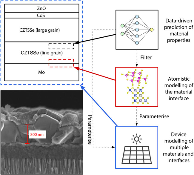
FIGURE 1. Image and schematic outlining the multi-layered structure of a typical Cu2ZnSn(S,Se)4 (CZTSSe) solar cell and the various approaches to interface modelling. The bottom left image is a Scanning Electron Microscope (SEM) image of a CZTSSe thin film photovoltaic device fabricated from nanoparticle inks. The length scale is indicated in red. The top left is a schematic of the same device, shown for clarity. The three boxes on the right outline three complimentary approaches to interface modelling: 1) (black boxes) data-driven approaches for predicting the properties of a single interface material; 2) (red boxes) atomistic modelling of the interface between two materials; and 3) (blue boxes) continuum modelling of the complete device, including multiple materials and interfaces. The dotted arrows indicate how these models relate to one another: lower accuracy data-driven predictions can be used as a initial filtering step before higher accuracy atomistic models are applied, and both of these approaches can be used to parameterise device models. The solar cell icon is a resource downloaded with permission from Flaticon.com.
The interfaces in a PV device are particularly important as they determine the carrier dynamics and so the overall device performance. (Edward et al., 1992; Franciosi and Van de Walle, 1996; Fritsche et al., 2001; Fritsche et al., 2005; Jaegermann et al., 2009; Li and Jen, 2022). To understand why this is one must first have a basic understanding of the processes underlying PV performance. Consider, for example, a solar cell with a planar structure: 1) a photon is absorbed and an exciton is created; 2) the exciton separates into an electron and hole; 3) the electron and hole travel through the absorber material; and 4) the electron and hole are extracted through an interface to their respective contact materials. The contact materials may be a metal contact, a buffer layer, a window layer, or an electron/hole transport layer. In addition, for polycrystalline materials there are additional interfaces in the form of grain boundaries. Before successfully reaching an external circuit to do useful work a charge carrier will need to traverse multiple interfaces.
There are several examples where interface engineering has improved the light-to-electricity efficiency of a device. To take one example, consider the development of CdTe solar cells. Most devices used a CdS buffer layer between the absorber material and transparent conducting oxide (TCO) until it was demonstrated in 2016 that replacing this with MgxZn1−xO led to improved performance. (Kephart et al., 2016). The reason for this improved performance is threefold and demonstrates the variety of functions an interface material must fulfil: the electronic band alignment with the TCO can be optimised with the proportion of Mg content, MgxZn1−xO allows for a higher temperature deposition of the CdTe which results in larger grain sizes and improved charge transport, and MgxZn1−xO has a larger optical band gap for better ultraviolet light transmission. (Kephart et al., 2016).
The rate of charge transport across an interface is primarily dependant on the energy band alignment of the constituent materials and the defects existing at the interface, so these are key considerations when optimising device designs. However there are additional considerations including chemical compatibility, heat transfer, (Sutanto et al., 2020), the mechanical stability provided by the interface layer and the rate of intended, or unintended, ion transport. (Prabhakar and Jampana, 2011). Whilst accurate computational predictions of the properties and processes within a single bulk material are now well established, (Oba and Kumagai, 2018), capturing the complex physics and chemistry at the interface between two materials remains an on-going challenge for theory and computation. (van der Giessen et al., 2020). In particular, linking microscopic structures and processes with material function is an inherently multi-scale problem that requires a range of approaches (Figure 1).
For materials design and optimisation where the structure of a material (or materials) is unknown there are a growing number of studies using the large amount of materials data that has already been generated and is readily available, or that can be generated using high-throughput-computing. For example, machine learning models have been used to predict thermodynamically stable quaternary oxides (Davies et al., 2019) and derive accurate force fields for molybdenum metal. (Chen et al., 2017). In the context of materials discovery, this data-driven approach can be used as a lower-cost filter before applying more expensive ab-initio models to the candidate interface material.
For modelling microscopic processes at the interface between two materials there are a range of atomistic simulation techniques based on either quantum chemical techniques or the equations of classical mechanics. These can also be used to calculate interface and bulk parameter values for device models. The typical size of unit cell used for interface simulations will depend on the process being modelled, the level of theory used and, unavoidably, the computer time that is available. The lower limit is on the order of hundreds of atoms, which has until recently restricted atomistic interface modelling to using classical potentials for describing the atom-atom interactions. However with recent research investment into high-performance-computing and the development of more computationally efficient codes, (Nakata et al., 2020; Prentice et al., 2020; Ratcliff et al., 2020), higher accuracy ab-initio quantum chemical predictions for systems with hundreds or thousands of atoms are now possible.
For predicting performance at the device level, continuum-scale models—most often Poisson-drift-diffusion simulations—are used. However capturing the full complexity of the processes at an interface in a numerical or analytical model at the device-level is not feasible. Instead it is most often assumed that the rate of charge transport is determined by the band offset energy between two materials and parameters (for example, the surface recombination velocity) which incorporate other microscopic physical effects. These values can be measured by experiment, calculated using atomistic simulations, or predicted using data-driven approaches, providing a straight-forward approach to multiscale modelling.
The focus of this review is interface modelling in thin-film PV devices. In particular, we are concerned with modelling planar interfaces between inorganic or hybrid organic-inorganic materials, rather than the bulk heterojunctions typically found in organic photovoltaic (OPV) devices or at grain boundaries. We do not consider mesoscale models that are designed to bridge between the micro- and macro-scale as although there are a limited number of applications in the context of hybrid perovskite photovoltaics, (Bahrami et al., 2021), these models have been most widely used within the OPV community where device performance is highly sensitive to the mesoscopic structuring of the bulk heterojunction.
We begin the review by introducing the key concepts underlying energy band alignment, which is the most important consideration for the design and optimisation of PV devices. We then go on to identify the other key features of an ideal PV interface material. In the second half of the review we introduce several approaches for modelling interfaces in PV devices: 1) data-driven methods for interface materials discovery and low-cost predictions of material performance; 2) atomistic interface models for a higher-accuracy understanding of processes at the microscale; and 3) continuum device models for understanding the combined effects of multiple interfaces at the device level.
2 Energy Band Alignment in Photovoltaic Devices
Electron energy level differences at an interface play a key role in a solar cell device. Their relative alignment describes built in electric fields that occur across material junctions, indicate the preferred direction of drift currents and also suggest potential tunnelling mechanisms. This all gives a greater insight and understanding to the workings of a device and the role the interface plays.
Semiconductor-semiconductor interfaces can be characterised in two groups: homojunctions and heterojuctions. Homojunction describes an interface where the two neighbouring bulk materials are the same, though the materials are often differentiated through dopant species or densities. On the contrary heterojunctions are comprised of two different materials. The latter comprise the bulk of this review as they are the most well-studied interface type in thin-film PV devices. Later in this section a discussion relating to metal-semiconductor junctions, and their classification as Schottky or ohmic is presented.
Our understanding of the interfaces within a device is very often summarised as an energy band diagram. Constructing energy band diagrams allows the observer to represent band-edge electron or hole energy levels, electric fields and current flow in the dimensions of energy and one-dimensional space; Figures 2, 6 are examples of energy band diagrams that will be discussed in more detail later in the paper. Many of the interesting features in energy band diagrams are at the interface region between two materials. The relative alignment at the interfacial regions of these diagrams can represent a range of features that are of importance in the design and fabrication of semiconductor devices, including: charge separation characteristics, interface bonding dynamics, interface trap states and depletion region widths.
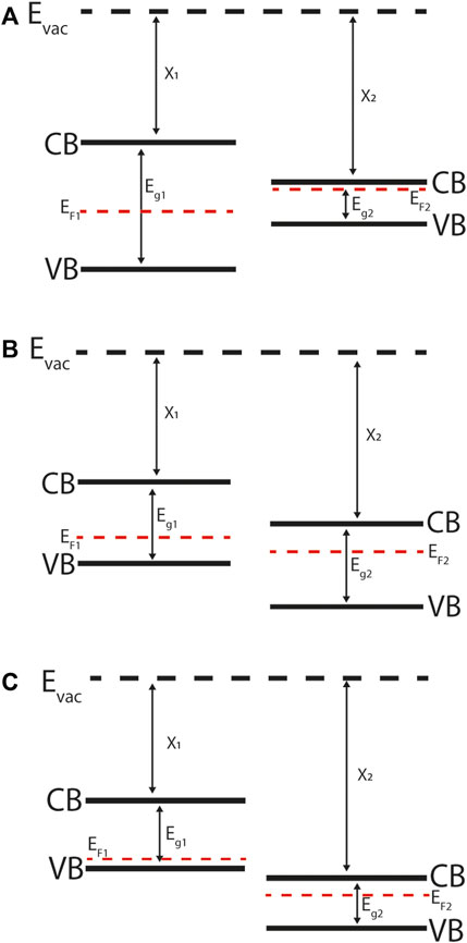
FIGURE 2. Energy band diagrams of abrupt semiconductor-semiconductor heterojunctions: (A) Straddling gap (Type-I), (B) Staggered gap (Type-II), (C) Broken gap (Type-III). Note that the materials are not in contact or in equilibrium with one-another, as indicated by the mismatch between their Fermi levels (EF). CB is the conduction band (minimum) and VB is the valence band (maximum) referenced to the vacuum level Evac. For quantitative predictions of band alignment the electron affinity (χ) and band gap (Eg) are used in the Anderson rule, which assumes that the vacuum level is constant.
Differences in the conduction band minimum (CBM) and valence band maximum (VBM) of neighbouring materials at an abrupt semiconductor-semiconductor heterojunction interface lead to band offsets. The type of band discontinuity depends on the electronic structure of the materials and are commonly grouped as: straddling gap (also known as Type I, Figure 2A), staggered gap (Type II, Figure 2B), and broken gap (Type III, Figure 2C). (Kroemer, 2001) Straddling gap junctions have conduction and valence band offsets of opposite sign, so that the lower CBM and higher VBM occurs in the same material. This structure promotes two-carrier processes such as radiative recombination as it is energetically favourable for the electrons and holes to occur in the same material. Staggered gap junctions have conduction and valence band offsets of the same sign, so that the lower CBM occurs in one material and higher VBM occurs in the other material, with an energy separation between the two. This structure promotes separation of electrons and holes, and so is of particular relevance to PV devices where charge separation underlies voltage generation. In broken gap junctions the CBM in one material drops below the VBM in another material and there a direct tunnelling mechanism across the interface.
For quantitative estimates of band offsets at semiconductor junctions the electron affinity rule introduced by (Anderson, 1960) is commonly used. This simple rule allows the band offset of the conduction band minima (ΔEc) and valence band minima (ΔEv) to be calculated from the bulk properties (band gap Eg and electron affinity χ) of the neighbouring materials. For example, consider Figure 2A where there is a straddling gap junction. In this case the band offsets are given by:
Anderson’s model is based on the assumption that the vacuum level is consistent when forming junctions between two materials. This rule is often used to calculate the band offsets, followed by Poisson’s rule to calculate the shape of the band bending that occurs upon carrier density equilibration across the heterojunction interface.
Semiconductor-metal interfaces are categorised differently given the absence of an electronic band gap in metals. They are classified as either Schottky or ohmic, depending on the difference between the semiconductor and metal work functions (Figure 3). For a p-type semiconductor with a work function greater than the metal, mobile charge will diffuse from the semiconductor into the metal and a Schottky contact will form. The resulting electrostatic field impedes majority carrier flow across the junction. For a p-type semiconductor that has a work function less than the metal an ohmic contact will form. Ohmic contacts promote majority carriers over the junction and are thus the ideal scenario for majority carrier extraction at an electrical contact.
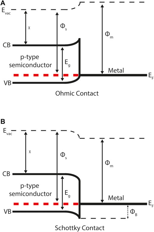
FIGURE 3. Energy band diagrams for a semiconductor-metal contact demonstrating: (A) ohmic behaviour (B) Schottky behaviour. CB and VB represent the conduction band (minimum) and valance band (maximum) respectively. ΦB describes the Schottky barrier height to majority carrier flow (in this case holes) across the junction. The Schottky-Mott rule can be used to calculate ΦB from the metal work function Φm and semiconductor electron affinity χ (both defined relative to the vacuum level Evac) and semiconductor band gap Eg. In equilibrium the Fermi-level Ef is constant across the semiconductor-metal interface.
The Schottky-Mott rule for semiconductor-metal interfaces is used to estimate Schottky barrier height ΦB from the metal work function Φm, semiconductor electron affinity χ and band gap Eg. (Francis Mott, 1939) For example, consider Figure 3 where there is a p-type semiconductor in contact with a metal. In this case the Schottky barrier height is given by:
It is important to note that both the electron affinity rule and Schottky-Mott rule can give only very rough estimates for band offsets as they ignore any chemical bonding, defect formation and electrical polarisation at the interface. These are highly idealised model that are only strictly valid in the limit of a large vacuum separation between the two materials.
For both semiconductor-semiconductor and semiconductor-metal contacts in thermodynamic equilibrium (where there is no illumination or external bias) the Fermi-level must be continuous across the interface. Physically this means that the electron or hole carriers will diffuse across the junction as a result of a concentration gradient. If the carriers were charge neutral this process would continue until there is a uniform distribution of carriers throughout the device. However, the carriers do carry charge and so they diffuse across the junction and leave behind charged ions. The charged ions form an electric field which eventually prevents further carrier diffusion. As a result of this process the conduction and valence bands exhibit band bending near the interface (Figure 3). There is no band bending in metals due to high concentrations of mobile charge carriers that can respond to the formation of an electric field.
For a semiconductor-semiconductor p-n junction in equilibrium the majority carriers (electrons in the n-type region and holes in the p-type region) diffuse across the junction as a result of their respective concentration gradients. This region at the interface is known as the depletion region (Figure 4) as it contains a built-in electric field which removes any free charge carriers. The width of the depletion region can be calculated using Poisson’s equation and is primarily determined by the doping density and dielectric permittivity of the material.
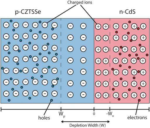
FIGURE 4. Depletion region schematic of the CZTSSe/CdS junction. The blue and red colouring represent p-type CZTSSe and n-type CdS respectively. The static charged ions—responsible for material doping—are also drawn. The depletion region does not contain any mobile charges. The black bar below denotes the material interface point (0), p-type depletion width (Wp) and n-type depletion width (Wn).
3 What Makes the Ideal Photovoltaic Interface Material?
Any interface model should be designed towards capturing the physical and chemical processes relevant to the application in question. In this paper we are considering the operation of a solar cell, and in the previous section we have considered the band alignment that is required for the correct distribution of charges in a PV device. In addition to this there are a host of other features required for optimised performance at a PV device interface. We will use a hole-transporting material at the metal-CZTS interface as a motivating example, although the features identified will, in many cases, be transferable to a range of applications and energy harvesting materials and are not solely limited to CZTS. In line with the majority of the literature, we will use CZTS to denote any compound of the form Cu2ZnSnSxSe4−x where x can take any value between 0 and 4.
CZTS thin film devices are based on the more established CIGS architecture in which the back contact material is molybdenum metal (Figure 5). As CZTS is a p-type material, the majority carriers are holes and it is these that must be extracted at the back contact. Molybdenum satisfies some qualities of a ‘good’ back contact: it maintains stability at high processing temperatures (Zoppi et al., 2011; Dai et al., 2014) and it has excellent adhesion with the substrate soda lime glass and CZTS absorber layer. However this picture is complicated through the sulfurization/selenisation process used to increase the efficiency of CZTS solar cells. During this process the Mo/CZTS structure is annealed on a substrate in a high temperature tube furnace (Qu et al., 2016a) and a barrier layer of Mo(S,Se)2 develops. (Qu et al., 2016b; Xu et al., 2018). The impact of this unintended barrier layer on device performance is still under debate in the literature, with some studies indicating that the formation of Mo(S,Se)2 can increase the ohmic nature of the back contact (Figure 6) and produce a contact with lower resistance (Salomé et al., 2010; Wu et al., 2012) providing the thickness of the Mo(S,Se)2 is not too large.
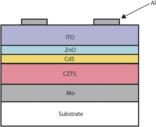
FIGURE 5. Typical copper zinc tin sulfide (CZTS) solar cell cross-section. From top to bottom: nickel and aluminium front contact grid, indium tin oxide (ITO), intrinsic zinc oxide (ZnO), cadmium sulfate (CdS), copper zinc tin sulfide (CZTS), molybdenum (Mo), soda lime glass substrate. The layer widths are not to scale.
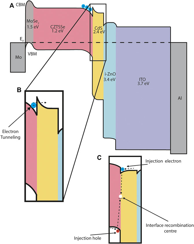
FIGURE 6. CZTSSe energy band diagram schematic. (A) The main panel shows the band alignment across the device. CBM and VBM represent conduction band minimum and valence band maximum respectively. The Fermi-level EF is denoted by a dashed line. The band gap for each material is given below each chemical formula. All material parameter data is taken from a previously published SCAPS simulation (Campbell et al., 2020). (B) Photocurrent resistance at a junction can produce a barrier to electron flow and reduce short circuit current, depending on the energy barrier height. For the CZTSSe/CdS interface a barrier less than 0.4 eV enables transport through a quantum tunnelling mechanism and is beneficial to device performance. (C) Alternative cliff-like band alignment at the CZTSSe/CdS interface. In this case injection electrons or holes (the diffusion current) are impeded by the large offset in available energy states and recombine at the interface. This causes a decrease in the reverse saturation current and a reduction in open-circuit voltage and fill factor.
3.1 Thermodynamic Stability
Thermodynamic stability against decomposition into competing phases is of primary importance, both in the design of bulk and interface materials. The key quantity here is the Gibbs free energy, as this is the value that is minimised for systems in thermodynamic equilibrium. (Jackson and Walsh, 2014). For an accurate understanding of stability the Gibbs free energy for all competing reactions, and at temperatures and pressures relevant for synthesis and device operation, should be considered.
Molybdenum is a commonly used contact material as it can withstand the high temperatures (500–600°C) required for annealing and, as such, provides more flexibility for device design. In contrast, oxides such as MoOx and NiOx have several decomposition pathways at high temperature and so require deposition in a superstrate configuration after the high temperature anneal.
In addition to establishing the thermal stability of a single material, we must also consider competing reactions at the interface. These reactant and products formed at an interface can incorporate species from each of the contact materials, widening the chemical space to be considered. For example, Scragg et al. have described the decomposition of Cu2ZnSnS(e)4 at high temperatures, both without (Scragg et al., 2012a) (Eq. 4) and with (Scragg et al., 2012b) [Eq. (5)] the presence of molybdenum.
The free energy change of the reaction with molybdenum [Eq. (5)] is calculated as -100 kJ and -150 kJ at 550°C, for Cu2ZnSnSe4 and Cu2ZnSnS4 respectively. These large negative free energies indicate that, at this temperature, the decomposition of CZTS(e) is thermodynamically favourable and that the CZTS(e)/Mo interface is unstable. This demonstrates why molybdenum thin films as a back contact have demonstrated less favourable characteristics, compared to CIGS, when paired with CZTS. It also highlights the importance of the processing techniques used to synthesise high-quality thin-films; in this case high processing temperatures are needed for the improvement of CZTS crystalline structure.
3.2 Matched Lattice Parameters
Strain at the interface between two materials is a potential source of instability which can impact on the defect, electrical and optical properties of each material. (Wu et al., 2021). When the strain is below a particular threshold value the material can alleviate the strain through defect formation, which then provide potential sites for charge capture and recombination. Above this value the interface can become incoherent with weak chemical bonding across the boundary. (Butler et al., 2016). The interfacial strain originates primarily from two types of mismatch: mismatch between the lattice constant of each material, and mismatch between the thermal expansion coefficient (α) of each material.
Lattice mismatch and strain related defects have been of particular importance in the development of high-efficiency III-V multijunction solar cells. With conversion efficiencies now approaching 50%, these cells are fabricated using epitaxial growth and careful control of the atomic-scale structure. (Li et al., 2021). A pre-requisite for good performance is that each absorber layer is lattice-matched to its neighbours, which is the predominant reason that the absorber layers in the highest-efficiency multijunction devices consist of closely related materials from the III-V compounds, such as GaAs, GaInP and GaInAs.
Various models have been introduced to rationalise the strain formed at the boundary between two materials and to identify alternative contact materials. For materials with the same crystal structure (for example III-V compounds in the zincblende structure) a comparison of the lattice parameters will suffice, whilst for materials with different crystal structures the comparison requires more subtlety. In 1984 Zur and McGill developed a reduction scheme based on the primitive lattice vectors of each material, (Zur and McGill, 1984), which has been more recently applied to a screening study for hybrid perovskite contact layers, (Butler et al., 2016), and implemented in the ElectronicLatticeMatch code. (Butler, 2017). To account for chemical bonding, which is neglected in the Zur and McGill scheme, more advanced theories that account for the atomic species on each lattice site are required. (Park et al., 2018).
Matched thermal expansion coefficients are also important due to the high annealing temperatures often used to enhance crystallinity and reduce defects in thin film PV; for example, CsPbI3 and CZTS are typically annealed at temperatures up to 330°C and 600°C respectively. These high temperatures result in a large temperature gradient during cooling to ambient temperatures. If combined with highly mismatched thermal expansion coefficients, a large thermally-induced strain results. (Wu et al., 2021).
In contrast to the lattice matching techniques introduced above, recent research has also harnessed the lattice mismatch between a material and substrate. This mismatch is used to facilitate a lift-off process, where the active material(s) are synthesised on a rigid substrate and then removed using physical, chemical or thermal methods. (Liu et al., 2021). For thermal lift-off processes the substrate is selected to have a different thermal expansion coefficient. When cooling a large stress field develops which is alleviated by the development of cracks parallel to the surface, and which eventually results in delamination of the active material. (Dross et al., 2007).
3.3 Energy Band Alignment
As already discussed, energy band alignment is also of critical importance, as this determines the rate of charge transport across an interface. At a metal-semiconductor junction the key quantity is the Schottky barrier height which relates to the difference in energy between the metal and semiconductor work functions. A contact is considered ohmic when the Schottky barrier height is non-existent or small enough to allow for unhindered transport of the electrons (for n-type materials) or holes (for p-type materials) across the interface.
At the CZTS back contact, there is evidence that the formation of a MoS(e)2 layer creates an ohmic contact with the CZTS layer. However the overrall PV performance may be reduced due to increased recombination of electron and hole charge carriers at the Mo/MoS(e)2 interface. The former observation is in line with research for closely related CIGS-based technologies, where it has also been suggested that MoS2 improves the ohmic nature of the Mo/CIGS back contact. (Wada et al., 2001; Polizzotti et al., 2013). However if the MoS2 layer is too thick this will be detrimental to device performance, resulting in a reduction in VOC and an increase in the series resistance. (Shin et al., 2012; Xu et al., 2019).
For CZTS an additional complication is the trade-off between thermodynamic stability of CZTS and the thickness of the MoS(e)2 layer. To prevent the degradation of CZTS through the loss of 2S(e) during high-temperature annealing, over-pressures of S(e) are used. However these high gas pressures cause the formation of a thicker layer of MoS(e)2 as a by-product.
Another important interface in CIGS and CZTS devices is the interface with the buffer layer, most commonly CdS. (Courel et al., 2014; Courel et al., 2015). There are two main types of conduction band offset (CBO) that occur at this interface: a positive, spike-like band alignment, where the buffer layer CB is higher than that of the absorber layer, and a negative, cliff-like, where the buffer layer conduction band (CB) is lower than that of the absorber layer (Figure 6).
In CIGS the most optimum CBO at the CIGS/CdS interface is, counter-intuitively, spike-like rather than cliff-like, providing that the barrier height is below 0.4 eV. This barrier allows electrons to tunnel through into the CdS, but does not produce a barrier to injection electrons under forward bias. The quantum tunnelling mechanism is described in more detail in Section 6.1. For cliff-like junctions, accumulated injection electrons under forward bias result in an increased recombination mechanism at the interface and a lower VOC. A spike-like energy barrier greater than 0.4 eV forms a significant barrier to current flow resulting in a dramatic decrease of the short-circuit current. (Minemoto et al., 2001; Campbell et al., 2020).
3.4 Electrically Benign Defect Formation
The formation of material defects, whether in the bulk or at interfaces, cannot be avoided in most materials. (Walsh and Zunger, 2017).
Furthermore, these defects can have serious unwanted implications in a PV device. Of particular concern are electrically active defect states that can capture electrons and/or holes, as these can lead to a reduction in the open-circuit voltage (VOC) and fill factor (FF), through processes such as Fermi-level pinning or non-radiative recombination.
The band bending model introduced in Section 2 effectively breaks down when we start to introduce material imperfections at the semiconductor-metal interface (Figure 6C). There are two possibilities that can arise at a metal-semiconductor interface: metal-induced states and semiconductor-vacuum states. In both instances electrically-active defect levels can be created within the semiconductor band gap, but each are associated with a different mechanism. In the former the states are created upon contact with the metal and are induced, for example, by lattice strain or chemical bonding. The latter are present on the surface of the semiconductor interface without contact to other materials.
Defect states in the band gap can cause a phenomenon known as Fermi-level pinning. Fermi-level pinning occurs when the interface defect states trap charge carriers that diffuse from the metal into the semiconductor. This effectively isolates the semiconductor from the effects of the metal and the semiconductor bands are aligned (pinned) relative to the charge neutrality level (CNL) of the interface defect states. This process adjusts the potential and electrostatic field at the interface, which in turn adjusts carrier transport across the interface. (Dimoulas et al., 2006).
In Ge-metal contacts Fermi-level pinning is a strong limiting factor in depositing contact grids with ideal electrical behaviour. The charge neutrality level (CNL) in Ge is situated close to the valence band (0.09 eV above EV), so that most acceptor states at the interface are filled at ambient temperature. (Dimoulas et al., 2006). As such, the Schottky barrier height that forms at this interface shows weak dependence on the particular metal used for contact to the electrical circuit. This is confirmed by a later study revealing that metal/p-Ge and metal/n-Ge junctions have ohmic and Schottky characteristics respectively, and both display a strong degree of Fermi-level pinning. (Nishimura et al., 2007).
Defects at the CZTS/CdS and CZTS/MoS(e)2 interfaces are abundant due to the low formation energies required for exchanging ion species of the same type (in this case, sulfur or selenium) across an interface. In addition, Cu and Zn have comparable ionic radii resulting in low formation energies for CuZn and ZnCu antisite defects in CZTS. This is compounded by the high annealing temperatures required for the growth of high-quality CZTS grains. (Chen et al., 2013). A large accumulation of antisite defects at the interface results in insufficient type inversion (the majority carrier being the opposite of its host layer) and weak band bending as an effect of Fermi-level pinning, whereby the Fermi-level is pinned close to the valence band at the interface. (Yuan et al., 2015). Cu-Zn disorder is also associated with band-tailing, where the measured band gap is less than that expected for the perfect bulk material. This fluctuation is dependent on the chemical purity of the precursor used to synthesise CZTS, and so the density of defects that are expected to be present. (Campbell et al., 2019).
Most studies of interfacial defects in CZTS solar cell devices focus on the CZTS/CdS or CZTS/MoS(e)2/Mo interfaces. (Kaur et al., 2017; Qi et al., 2017; Suryawanshi et al., 2017; Campbell et al., 2018; Kim J et al., 2020). Defects that are particularly detrimental to performance are observed at the CZTS/CdS interface, where a high concentration of defects results in cliff-like band alignment and high non-radiative electron-hole recombination rates. This is also observed at the CIGS/CdS interface. (Kaur et al., 2017).
In addition to defect formation at semiconductor-semiconductor and semiconductor-metal heterojunctions, CZTS, CIGS and halide perovskite thin films are particularly prone to the development of grain boundary (GB) defects. (Yan et al., 2007; Li et al., 2011; Park et al., 2019). Not all GB defect formation is problematic; for example there is evidence that GBs in CIS-based materials are beneficial to device performance. (Yan et al., 2007). In contrast, the defect states associated with GBs in CZTSe are located in the band gap and as such provide sites for charge trapping and recombination. (Li et al., 2011). Similarly, the GBs in halide perovskite materials are detrimental to device performance in that they provide energetically favourable sites for the formation of iodine interstitial defects, which in turn act as a site for charge trapping and recombination. (Park et al., 2019).
3.5 Favourable Ion Transport
Ion transport, when compared to electronic transport, is not as central to the functioning of a solar cell. However it can still influence the performance of a device through material doping and charge accumulation. For some materials, such as CZTS and CIGS, ion diffusion can increase the cell performance. In others, such as the halide perovskites, ion migration can lead to decreased performance. Examples for both extremes will be given in this section.
CZTS based solar cells are often fabricated on a soda lime glass (SLG) substrate, which primarily provides mechanical support to the cell. This results in sodium from the SLG also diffusing through the device into the MoSe2, Mo and CZTS layers, leading to a notable improvement in the conductivity of the CZTS layer. (Prabhakar and Jampana, 2011). In a study comparing SLG to other substrates, the carrier concentration in CZTS increases by an order of magnitude (6.1 × 10¹⁶ to 35.4 × 1016cm−3), leading to a significant increase in conductivity (from 41.2 to 58.4 Ωcm−1). (Prabhakar and Jampana, 2011). The underlying reasons for this increased carrier concentration has been examined using first-principles calculations. Wei and Zunger determined that sodium on a copper site (NaCu) results in an injection of holes into the system, increasing the hole density and thus the conduction of the CZTS p-type absorber layer. Sodium intercalation has also been associated with an increase in crystallite size, reducing the grain boundary area which in turn reduces the number of locations for non-radiative carrier recombination. (Prabhakar and Jampana, 2011). This same relationship has been observed in CIGS films fabricated on soda lime glass substrates. (Contreras et al., 1998).
Another source of beneficial ions in a CZTS cell is at the molybdenum rear contact. During the sulfurisation/selenisation process molybdenum is exposed to temperatures between 500–600°C, at which the molybdenum crystal structure should be relatively unchanged. However there is a clear temperature-dependent diffusion of molybdenum into the CZTS layer, with sulfurisation at 600°C leading to a more Mo-rich CZTS interfacial layer and PV efficiencies five times greater than materials formed via sulfurisation at 500°C. These studies demonstrate the importance of contact materials being able to maintain a stable crystal structure whilst still allowing beneficial ion diffusion throughout the device.
On the other hand, ion diffusion in perovskite-based PV negatively affects stability, performance, and effective working lifetime. Hybrid halide perovskites (ABX3) are categorised as mixed conductors meaning they possess both electronic (Leijtens et al., 2015a) and ionic conductivity, (Eames et al., 2015; Egger et al., 2015; Yang et al., 2015), a phenomenon which has been extensively studied in recent years. (Xiao et al., 2015; Xu et al., 2015; Thomas et al., 2016). Ion transport in these materials is the primary contributing mechanism for I-V hysteresis (Meloni et al., 2016) and poor thermal stability, (Leijtens et al., 2015b; Zhao et al., 2016), leading to performance degradation over time. (Leijtens et al., 2015c). These materials also display a coupling between electrical and ionic behaviours, with increasing light intensity causing a reduction in the activation energy for ion migration. (Zhao et al., 2017).
In this section we have outlined several properties and processes at the interface that impact on device performance. We note here that this is a challenge not only for materials design, but also for materials process engineering. For example, to reduce the concentration of electrically active point defects various strategies have been developed: selecting high-quality precursors for materials synthesis, (Campbell et al., 2019), incorporating additional dielectric passivation layers, (Kim et al., 2017), or using post-deposition annealing. (Fritsche et al., 2005; Jaegermann et al., 2009).
We also note that our ‘wish-list’ for an ideal PV material is somewhat incomplete and could be extended to include other factors we do not mention here. This includes thermal transport properties (the rate of heat transfer), mechanical properties (elastic modulus and deformation) and optical properties (band gap and absorption coefficients). On the prior point we draw the readers attention briefly to Figure 6, which shows a series semiconductor materials with increasing band gap as we move between the back metal contact (Mo) and the front metal contact (Al). Increased optical band gaps result in increased ultraviolet light transmission and more light energy available for conversion within the absorber material.
In the next three sections we review methods for modelling the interface between two materials. We begin with a short section on chemical heuristics—using simple chemical rules to reduce the vast compositional space of possible interface materials. We then review atomistic methods for understanding at an atomistic level the complex physical and chemical processes at an interface. Finally, we outline the theory and techniques for modelling interfaces at the device level.
4 Data-Driven Approaches to Interface Materials Modelling
A common approach when developing a photvoltaic absorber material is to integrate the new material into the existing device architecture for a related compound. For example, CZTS in the kesterite structure is derived from CIGS in the chalcopyrite structure. As a result of this relation, CZTS thin film devices are based on the CIGS architecture with a CdS window layer and molybdenum back contact. However this transfer between technologies is unlikely to lead to a optimal material pairing because, as we have discussed above, processes at an interface are highly sensitive to the specific structural, electronic and defect properties of a material.
The opposite data-driven approach is to widen the search space to include all possible interface materials, and then apply a sequence of computational filters to identify those with a set of pre-defined target properties. The initial filters may include low-cost chemical rules (also known as chemical heuristics) to reduce the search space. For example, if searching for a binary material we might enforce the first Pauling rule, requiring that the ratio of the anion and cation ionic radii falls within a certain range. (Pauling, 1929). Alternatively, the filters may not derive from chemical knowledge but from statistical (e.g machine learning) models built on a large dataset of material properties. An advantage of the screening approach is that additional constraints can be implemented in the workflow. For example, the Herfindahl Hirschman index can be applied to select for compounds which contain abundantly available elements, (Mansouri Tehrani et al., 2017), or compounds containing toxic elements can be removed at an early stage.
When an atomic-scale structure is yet to be determined the computational model must be able to make predictions based on elemental composition only. In the context of interfaces in solar cell devices we are particularly interested in predicting the electronic properties of materials, such as the CBM and VBM referenced to the vacuum level, and the electronic band gap. Chemical rules connecting elemental composition with electronic structure have a long history starting with the work of Mulliken who developed an absolute scale of atomic electronegativity (defined as the mid-point in a semiconductor band gap) in 1934. More recently, Pelatt et al. proposed the Atomic Solid State Energy (SSE) scale as an alternative approach to electronegativity. (Pelatt et al., 2011). This is derived from data for the ionisation potentials and electron affinities of 69 binary semiconductors containing 40 different elements. By considering the energy difference between the most negative cation SSE and the least negative anion SSE, this method provides estimates for the absolute CBM, VBM and band gap in any compound. The SSE scale has been used as a filter in a high-throughput search for photoactive chalcohalide semiconductors, identifying two new compounds with band gaps in the visible spectrum, (Davies et al., 2018), and to rationalise the measured hole concentrations in Cu-based chalcogenide PV absorber materials. (Itthibenchapong et al., 2013).
The SSE scale is based on a linear trend between the electron affinity and ionisation potential versus band gap. However for many properties of interest the trend is not so readily recognisable as there may be a higher number of dependent parameters and/or more complex non-linear relationships. In this case machine learning (ML) can be used to identify relationships in the data and develop predictive models.
The number of studies based on ML applied to materials science is growing quickly. This is driven by investment into high-performance computing, freely available materials databases [for example the Materials Project (Jain et al., 2013) or OQMD (Kirklin et al., 2015)] and open-source machine learning libraries. A common approach is to use well-known chemical concepts, such as ionic radii or electronegativity of the constituent elements, as features for supervised machine learning. This approach has been used in a number of studies to predict the electronic band gap across a range of potential materials for solar applications, including: double chalcogenide perovskites, (Agiorgousis et al., 2019), orthorhombic lead-free perovskites, (Lu et al., 2018), wurtzite nitride semiconductors (Huang et al., 2019) and kesterite materials. (Weston and Stampfl, 2018). The predictive power of the machine learning model depends on there being a training database of suitable size, hence the reliance on either existing materials data or high-throughput computing resources.
ML has also been used in the development of interatomic potentials. Here the ML model is trained to predict energies and forces from first-principles calculations of small systems (tens or hundreds of atoms). The ML-based potential (MLP) is then used to model large systems (thousands of atoms) that are intractable for first-principles simulation. This approach has particular relevance to interface materials where amorphous and nano-structured phases can be formed which require large periodic unit cells for building accurate models. For example, a MLP for molybdenum has been developed that achieves close to DFT accuracy for a broad range of properties including elastic constants, phonon spectra and surface energies. (Chen et al., 2017). This MLP is based on the spectral neighbor analysis potential (SNAP) developed by (Thompson et al., 2016) It also incorporates well-established, domain-agnostic machine learning techniques: principal component analysis for the structural selection process, and a differential evolution algorithm for optimizing the model hyperparameters.
The studies introduced so far in this section have been used to predict the properties of a single material. There are also a small number of studies that use ML to predict the chemical and structural changes that occur when two materials join to form an interface. For example, ML has been used to predict the structures formed at epitaxial inorganic interfaces typical of high-efficiency III-V PV materials. This technique uses surface matching accelerated with Bayesian optimisation to predict the interfacial distance and potential energy surface at a fraction of the computational cost required by the equivalent DFT calculations. (Moayedpour et al., 2021). It is also possible to use a MLP to describe interface bonding if a suitable training set is used. There are various cases in which this approach has been used to describe systems where the interface region is small, such as in supported nanoclusters. (Artrith, 2019). Modelling the interface between two extended crystalline materials is more challenging as this typically requires larger simulation cells to generate the training data. The grain boundaries in aluminium have been modelled using a MLP which was trained using structures optimised using conventional interatomic potentials and density functional theory. (Tamura et al., 2017). This allowed the prediction of minimum energy structures for extended grain boundary structures that would not have been accessible using DFT alone. There is not yet, to our knowledge, extension of this approach to other materials or heterogeneous interfaces.
The on-going challenge for materials simulation is the trade-off between accuracy and computer time. The common theme across all of the ML-based studies introduced in this section is that they aim to provide predictions with the accuracy of ab-initio quantum chemical simulations but at lower cost. Although this computational efficiency has been established for accurately predicting the properties of a single material, there has been minimal data-driven research which explicitly considers the bonding and structural changes at a PV interface. For these research problems the most commonly used approach is classical or quantum atomistic simulation, which is the subject of the following section.
5 Atomistic Modelling of Photovoltaic Interfaces
Given that materials interfaces represent major bottlenecks to the performance and stability of PV devices, their accurate simulation and understanding at the atomistic scale are becoming ever more important. However, compared to the modelling of bulk crystalline materials, the methods for modelling interfaces in PV materials (and indeed other energy materials) are far less developed and often do not present the same reliability and computational efficiency. While bulk crystalline materials are modelled atomistically as infinite lattices using three-dimensional periodic boundary conditions, simulations of the heterogenous interfaces in PV devices require the preparation of surface slabs that are placed in direct contact with each other. The development of such interfacial models is challenging and careful consideration must be given to their scale, alignment, chemical composition, stability, disorder/defects and thermal and mechanical damage to ensure that they are reliable and representative of real interfaces. Nevertheless, despite the challenges they present, the atomistic modelling of interfaces can offer a wealth of valuable information regarding the performance of PV materials and devices at an atomic resolution, as well as the potential for the discovery of unique behaviour and properties not exhibited in bulk materials.
Thermodynamic stability is one of the most fundamental properties for defining the pertinency of a given interface. The first factors to consider when creating an interfacial model are surface formation and the energy it requires, i.e., the surface free energy (γsurface, J m-2). γsurface defines the energy required to cleave a bulk material and form a surface with a particular Miller index and can be calculated using both forcefield or electronic structure methods, as exemplified in many atomistic modelling studies of PV materials. (Raymand et al., 2008; Wang et al., 2015; Nicholson et al., 2020). Such a surface can then be modelled as a slab consisting of a number of atomic layers converged with respect to the calculated internal energies from DFT or a forcefield approach. Several approaches have been proposed to reduce the computational expense of converging the slab thicknesses, including orientating the reference bulk material with the Miller index of the surface of interest (Sun and Ceder, 2013) and saturating any dangling bonds with pseudo-hydrogens based on fractional core and electronic charges. (Sai et al., 2018). By combining the γsurface values for a selection of Miller index planes, the Wulff construction, which minimises the surface energy for a given enclosed volume, can be used to predict the equilibrium particle morphologies of PV materials. (Barnard and Curtiss, 2005; Wilson et al., 2016).
The energy of an interface (γinterface) can also be obtained using a similar method to that for γsurface using the computed total energies of the interface and its corresponding bulk materials. Like γsurface, γinterface must also be converged with regards to system size, which can represent a substantial computational cost, particularly for quantum mechanical simulations. The sign of γinterface signifies whether the interface is more (negative value) or less (positive value) stable than the respective bulk materials in isolation. This method has been used to provide significant insights into the stability of the interfaces of PV materials, for example CZTS/CdS (Rondiya et al., 2019; Rondiya et al., 2020), CCTS/CdS (Rondiya et al., 2020) and TiO2/hybrid perovskites. (Mosconi et al., 2014). In addition to heterogenous interfaces, γinterface is equally applicable to homogenous interfaces and has been widely applied to investigate the stability and formation of grain boundaries in various PV materials. (Park and Walsh, 2021).
As discussed earlier in the review, the alignment of bands between different materials is critical to the performance of devices with semiconductor heterojunctions. Quantum mechanical simulations play an important role in predicting and optimising band alignment and the most used approach to provide a comparison with experiment is the use of slab models. (Singh-Miller and Marzari, 2009; Peng et al., 2013). In this approach, the electrostatic potential in the vacuum provides a reference so that the ionisation potential can be calculated using the valence band maximum of the slab model. One issue that can arise from the use of slab models based on ideal surface cuts in calculating the ionisation potential is the presence of dangling bonds. Although these surface states mean that the ionisation potential from a single slab does not represent the true ionisation potential from the bulk material, their effect can be corrected for by using the calculated valence band maximum of the bulk material and surface dipole of the slab. (Peressi et al., 1998). It is also important to bear in mind that the use of idealised surface models does not take into account the effect of impurities (either added intentionally or otherwise), which can have a dramatic effect on the electronic properties of the interface. (Davis et al., 1980; Ming et al., 2018; Borchert et al., 2019).
In addition to the use of explicit interfacial models, two alternative approaches have been utilised for the calculation of band alignment via atomistic modelling. The first is the natural band alignment approach, where the band offsets are obtained by explicitly calculating the heterojunctions of the semiconductors of interest. While this approach has the advantage of allowing for facile comparison with spectroscopic analyses, it is only appropriate for materials with similar structures and compositions due to the assumption of transitivity for the band offsets. (Butler et al., 2019).
This method has been successfully applied to investigate band alignment in a wide variety of PV materials, including II–VI and III–V semiconductors (Wei and Zunger, 1998) and hybrid perovskites. (Butler et al., 2015). The second technique utilises the branch-point energy, which is defined as a level at which defect states in the band gap change from donor-like to acceptor-like states, to align bands across bulk semiconductors. This can be achieved by calculating the band gap centre, which represents the average of the VBM and CBM across the Brillouin zone (Toroker et al., 2011). Although this approach is relatively straightforward, computationally inexpensive and has been applied to a large selection of oxide and nitride PV materials, (Schleife et al., 2009), it is highly sensitive to the choice of computational parameters. (Alidoust et al., 2014). In-depth reviews of these methods and their application to PV interfaces are available elsewhere. (De Angelis, 2014; Even et al., 2014; Park and Walsh, 2021).
It is also noteworthy that atomistic modelling can also potentially be used to assess a variety of other important properties that govern the performance of PV interfaces beyond thermodynamic stability, electronic structure and band alignment, such as ion transport, defects and degradation mechanisms. However, despite the importance of these properties and the fact they have been routinely simulated in individual PV materials (Oba et al., 2008; Eames et al., 2015; Lanzetta et al., 2021) and grain boundaries (Park and Walsh, 2021) using both classical and quantum methods, studies of their effect on PV heterointerfaces are at best scarce. This is primarily because of the inherent challenges in modelling interfaces discussed throughout this review.
Due to their own unique advantages and disadvantages, the application of both forcefield and electronic structure calculations is vital in closing the current gap between bulk and interfacial modelling in terms of practicality, efficiency and accuracy. The need for larger atomistic models that can be simulated for longer timescales is one of the most critical challenges currently facing the modelling of interfaces and this is where classical techniques, such as molecular dynamics, have a distinct advantage. Such models can also be parameterised using DFT and ML calculations to improve their accuracy and reliability. In contrast, there are clearly many properties, e.g., band alignment and charge transfer, where the electronic structure of the interface must be considered explicitly and the use of classical forcefields is not appropriate. The understanding of the interfaces in PV devices is inherently a multi-scale problem and therefore require multi-scale approaches to solve it.
6 Continuum Scale Models of Photovoltaic Devices
The simulation of a complete solar energy conversion system is a macro-scale problem that requires us to consider several material interfaces. In previous sections we have discussed modelling material structure and composition both in a bulk interface material, and at the interface itself. Here we consider models at the device level, which can incorporate several material interfaces, and include simulations up to the scale of module installations.
There are several approaches for calculating the electronic properties of a device. At the simplest level there is the detailed balance approach, which in some formalisms only requires the energy and absorptivity of the absorption edge. For increased accuracy, but where a detailed knowledge of the device structure is unknown, a diode model can be used. In this case, the various transport and recombination mechanisms can be modelled using electrical components. However the most fundamental and accurate method for predicting electronic behaviour is Poisson-drift-diffusion (PDD). This underlies the large majority of software tools used for modelling PV devices, and is the focus of the following section. Following this we summarise and discuss some of the key software packages used for device modelling and identify opportunities for accelerating our ability to model interfaces in a increasingly diverse array of PV devices.
6.1 Equations Governing Device Level Behaviour
The most fundamental equation for predicting electronic behaviour in semiconductor devices is the Poisson equation, which relates the electrical charges in the structure to the electrostatic potential ϕ. In a semiconductor the charge is typically split onto four density domains: electron density n, hole density p, acceptor atom density
where ϵ is the dielectric permittivity of the material. The continuity equations are used in conjunction with Poisson statistics. The continuity equations are book-keeping equations in that they ensure conservation of charge, balancing the carriers that enter and leave different parts of the model. The continuity equations for free electrons in the conduction band and holes in the valence band are given by the following two equations:
where Jn is the electron current density, Jp is the hole current density, G(x) is the generation rate (for a solar cell this will be generation from illumination) and U(x) is the net recombination rate. The recombination rate may incorporate several mechanisms including radiative band-to-band recombination, defect mediated Shockley-Reed-Hall recombination, Auger recombination and surface recombination at the interface between materials. The equations describe a steady-state system where the change in current is exactly balanced by charge generation and recombination.
The transport equations describe the dynamics of the carriers and therefore also the current in a solar cell. Current in a solar cell can be broken down into two parts: a drift component due to the electric field
where the as-yet undefined constants are material-specific transport parameters: μn is the electron mobility, μp is the hole mobility, Dn is the electron diffusivity and Dp is the hole diffusivity.
The above equations are well-established equations for semiconductors that are derived and expanded on in many semiconductor textbooks [for example, Reference (Nelson, 2003)]. They form a coupled system of nonlinear partial differential equations which do not, in general, admit analytical solutions for systems of interest. Instead, numerical techniques are used to model the behaviour or these systems for given material types and geometries. These numerical techniques are all based on the discretisation of a device in both space and time yet can be approached in a variety of ways, such as the well-established and robust finite difference method, or the finite element method which is more flexible in terms of problem geometry. In addition, there are various alogrithms which implement each method. For example, the finite element method can be implemented using the Gummel method for fast convergence, or the Newton method when there are high recombination rates leading to strong coupling of the continuity and Poisson equations. (Liu et al., 2011). Once solved, the equations describe the movement of charge carriers and their relationship with current and electric field strength.
In addition to the classical physics introduced above, quantum tunnelling should be considered for the accurate prediction of charge transport behaviour across heterojunctions where either the material layer or depletion layer is thin (typically less than 15 nm). Quantum tunnelling can affect the calculated current as it results in the transport of electrons across a potential barrier even if the electron energy is less than the barrier height—transport that is forbidden in the classical regime. Experimental measurements demonstrate that quantum tunnelling mechanisms can dominate the charge transport current behaviour in a cell and can significantly impact the PV performance when there is a spike-like barrier at the interface. (Verschraegen and Burgelman, 2007). For a full description of quantum tunnelling, electrons with an energy below the potential barrier can be represented by the Schrödinger equation and solved to give wave vectors and a tunnelling probability. This however requires computational resources beyond that typically used for device level simulations, and so analytical approaches such as the WKB method are commonly used to give approximate corrections to the calculated current. (Burstein and Lundqvist, 1969; Gundlach and Simmons, 1969; Verschraegen and Burgelman, 2007).
There are also multi-scale device models that incorporate methods for solving the Schrödinger equation directly. These models are motivated by the increasing amount of research and development into solar cell devices based on nano-structured materials, such as quantum dot, nanowire or quantum well structures. These materials consist of multiple nanometre thin layers which can, as a result of being ultra-thin, accommodate large amount of strain at the interface. (Kroemer, 2001). Research interest is driven by their potential for increased conversion efficiencies over single-junction cells without the complexity of multi-junction designs. In several software packages (Birner et al., 2007; Alonso-Álvarez et al., 2018) the quantum properties of the nanostructures are calculated by solving the one-dimensional Schrödinger equation to give the eigenvalues and eigenvectors associated a given potential. To include local strain fields that develop as a result of lattice deformation the electron mass can be modified. (Birner et al., 2007; Alonso-Álvarez et al., 2018). It is also possible to repeatedly iterate through the Schrodinger and Poisson equations until a self-consistent solution that takes into account the classical and quantum mechanical charge densities has been found. (Birner et al., 2007).
As discussed further in the following section, these classical and quantum techniques are implemented in several software packages which are designed to output useful semiconductor characterisation data that can be directly compared to experimental results. Notable examples relevant for PV research include current-voltage (J-V) characteristics, internal quantum efficiency (IQE) and external quantum efficiency (EQE) and there are also software packages that can make predictions for more advanced characterisation techniques such as capacity-voltage and photoluminescence. (Froitzheim et al., 2003).
6.2 Solar Cell Modelling Packages
There are numerous packages to simulate crystalline, polycrystalline and nano-engineered PV cells. Many of these are well documented and have yielded significant insights whether paired with experimental results (Karthick et al., 2020; Houimi et al., 2021) or as stand-alone simulations. (Verschraegen and Burgelman, 2007; Feng et al., 2013; Mostefaoui et al., 2015). Whilst these packages tend to simulate the same sets of solar cell characterisation data (for example, current-voltage curves) they are differentiated by both the approach they use and the applications they are tailored towards. For example, nextnano (Birner et al., 2007) uses the finite element method and is particularly suited to the diverse geometries of nano-engineered materials. In contrast, PC3D uses a fourier transform solution to the drift-diffusion equations which is computationally efficient but more restricted in its applications. (Basore, 2020).
Table 1 summarises some of the other notable software packages for PV device simulation. The packages listed are capable of exploring several aspects of solar cell device behaviour, with the primary focus being on semiconductor physics. In addition to those listed in the table there are packages tailored towards simulating other sub-sets of the PV energy generation process, including SMARTS to calculate the solar spectrum as a function of atmospheric conditions, (Gueymard, 1995), OPTOS for light absorption at the module level (Tucher et al., 2016) and PVlib for module and systems level modelling. (Holmgren et al., 2018a).
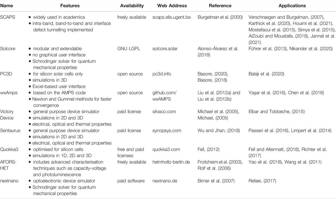
TABLE 1. A non-exhaustive list of solar cell device simulation tools. The table allows a comparison of the key features and availability. Unless otherwise stated, the simulations are one-dimensional and a graphical user interface is available. ‘Open source’ indicates that the source code is available for free download. ‘Freely available’ indicates that the compiled software is available for free download. Note that Solcore is free to use and is distributed with an open source license, GNU LGPL (gnu.org/licenses/lgpl-3.0). We also include signposts for further information: a project web address and a reference in the academic literature. Finally we list selected publications in which the software has been applied.
The availability of each code is also listed in Table 1. The general purpose device simulators, capable of modelling a whole host of semiconductor devices including memory devices and power electronics, are proprietary and require a paid license. Of those listed that are freely available, only Solcore is distributed with an open source license (GNU LGPL, gnu. org/licenses/lgpl-3.0) although the source code for PC3D and wxAmps is openly available. Two of the software packages listed, Quokka3 and PC3D, are heavily geared towards silicon devices, and are the only freely available packages listed for simulations in three dimensions. The user interfaces come in a variety of forms: Solcore provides a library of tools which are called directly in a Python script, PC3D uses an excel-based user interface, whilst others (including SCAPS, wxAmps and AFORS-HET) provide a graphical user interface.
The list of simulation codes in Table 1 is not exhaustive. Several groups develop their own in-house codes tailored towards particular research problems, some of which have been developed and published in public code repositories. (Holmgren et al., 2018b; Juan, 2022; Koopmans and Vincent, 2022). These codes generally provide command line interface (CLI) or application programming interface (API) to underlying routines, and as such require a basic familiarity with programming. Script-based simulation tools are also more suitable for problems that use high-performance-computing or cloud computing on remote machines.
In the following sections we compare the simulation capabilities and use cases of SCAPS-1D and Solcore. These have been chosen for greater discussion as they provide contrasting approaches: SCAPS-1D is a well-established device level simulation package that is widely used in the experimental community, whilst Solcore is a highly modular, Python-based extensible open-source package that aims to provide flexibility for those who wish to develop and extend the code for their own research purposes.
6.3 Solar Cell Capacitance Simulator-1D
SCAPS (Burgelman et al., 2000) (a Solar Cell Capacitance Simulator) is one of the most widely used software tools for simulating solar cell device characteristics. (Verschraegen and Burgelman, 2007; Mostefaoui et al., 2015; Simya et al., 2015; AlZoubi and Moustafa, 2019; Karthick et al., 2020; Houimi et al., 2021; Jannat et al., 2021).
It was originally developed at the turn of the millenium for polycrystalline cell structures of the CIGS and CdTe family of materials, and is maintained by researchers based at the Department of Electronics and Information Systems (ELIS) of the University of Gent, Belgium. (Burgelman et al., 2000). It is designed to accommodate multiple thin films and interfaces, and has evolved over the years to include additional mechanisms for recombination (for example, Auger recombination) and tunnelling (for example, tunnelling at interface defects). As is common with the other software packages listed in Table 1, SCAPS-1D solves Poisson’s equation along with the continuity equations to describe carrier transport physics and calculate quantum efficiency (QE) and J-V characteristics. It can be used to describe imperfect materials through the specification of various parameters including recombination and capture rates at defect centres, and defect densities. This provides quantative predictions for the recombination current and points to which recombination mechanisms in a device a particularly limiting to device performance.
The primary advantage of SCAPS-1D is in terms of accessibility. SCAPS-1D is fully self-contained and free to download, is straight-forward to install on a modern operating system and is distributed with a graphical user interface so that those without any familiarity with programming can use it with ease. The lightweight (in terms of computational expense) and accessible nature of the programme, yet ability to model multiple thin-film layers and interfaces, has led to it being applied in several studies of potential interface materials. For example, Campbell et al.(Campbell et al., 2020) use SCAPS to compare CdS and In2S3 as the buffer layer in a CZTSSe cell. Combined with optical and electronic characterisation techniques they establish that although In2S3 has the more favourable band alignment, the presence of interfacial defect states results in a lower overall VOC.
6.4 Solcore
Solcore is a complete semiconductor solver written in Python 3 and developed by researchers at Imperial College London. (Führer et al., 2013; Alonso-Álvarez et al., 2018; Nikander et al., 2020).
The packages are arranged in a modular manner, with modules dedicated to materials science (including a material parameters database and quantum solver), optical methods, light sources, solar cell calculators and a large-circuit solver. Together these modules provide optical and electronic solving capabilities for a wide range of solar cell materials, with specific attention placed on III-IV devices, such as GaAs, and semiconductor nanostructures where quantum confinement effects are dominant. As such, Solcore is a multi-scale tools that extends from the micron length scales of light propagation to module-scale performance characteristics.
Device characteristics in Solcore can be predicted using a range of techniques (detailed balance and the diode equation), the most accurate being PDD as introduced above. A key advantage of Solcore is that it is designed for integration with external libraries. One such library is SMARTS (Gueymard, 1995) which incorporates a model of the atmospheric transfer of radiative sunshine. This allows for an accurate description of the solar irradiance depending on atmospheric conditions (such as water vapour, nitrogen dioxide, ozone or uniformly mixed gas absorption) along with other modelling capabilities such as Raleigh scattering, light diffusivity and back scattered light rays. Solcore is somewhat unique in that it has been designed with user extension and adaptation in mind: code development takes place in a public facing Github repository, the code has a modular structure, and Solcore ‘bootcamps’ have been organised for training and community building purposes. This is in contrast to the majority of simulation packages that are often high level, self-contained and do not invite extensive customisation.
Solcore has been applied to a number of research problems that incorporate multi-junction, quantum well and light-trapping technologies. For example, Pearce et al. use Solcore for the development of a perovskite on silicon tandem cell, where the perovskite top cell is deposited conformally onto the pyramidal surface of a silicon cell. (Pearce and Ekins-Daukes, 2019). Solcore has also been used in the development of ultra-thin GaAs cells for space applications. Here the challenge is to develop cells which are both physically thin (for radiation resistance) yet optically thick (for strong light absorption). Sayre et al. used the Solcore optical and solar cell modules to model and optimise these novel structures. (Sayre et al., 2022).
These examples demonstrate some important points about the role software design plays in enabling science. In the study from Pearce et al. the Rayflare software package used Solcore’s light source module and Structure class to calculate light absorption in a challenging geometry. This was made possible through the interoperability of each code, a feature which will become increasingly important in the quickly growing ecosystem of open-source tools for PV. (Holmgren et al., 2018c; Ayala Pelaez and Deline, 2020; Kim S et al., 2020; Silva et al., 2022). In addition, the development of PV devices for niche applications, such as high-efficiency and radiation-resistance solar cells for space, highlights the importance of code extensibility and adaptability. For example, researchers in the field of space PV may wish to extend a code to include physical models particularly relevant at ultra-thin length scales, such as carrier recombination at radiation induced defect sites.
Within both Solcore and SCAPS-1D there are assumptions that are made about the device so that the Poisson statistics and continuity equations can be used. For example, the solver in Solcore uses the Boltzmann approximation for carrier distribution with the assumptions that carrier concentrations are not highly doped, all carrier populations are in quasi-thermal equilibrium, and that the mobility of carriers are completely independent of the electric field. As a direct result of this latter assumption the Poisson drift diffusion model is only valid in weak electric fields. The various assumptions and model limitations inherent in all device modelling highlights the need for clear software documentation and on-going communication channels between software developers and users.
The accuracy of predictions made at the device level are always limited by the complexity of the atomic-scale interactions at the interface. For example, device models commonly assume that the work functions and electron affinity of the bulk materials govern the band bending observed on energy diagrams. However, as we have discussed earlier in this review, heterojunctions experience interface-specific bond formation, and this is especially true for polycrystalline materials that are prone to defect state formation at interfaces. (Raymond and Kronik, 2018). When the specifics of material-material interaction are not accounted for in device level models there will always be an inherent limitation to the accuracy of any predictions made.
7 Conclusion
As Herbert Kroemer famously wrote in his Nobel lecture, ‘The interface is the device’. (Kroemer, 2001). For solar cells, where charge transport across several heterojunction interfaces is a pre-requisite for working devices, this quote is particularly pertinent. However, despite material interfaces representing a bottleneck to the performance and stability of PV devices, their accurate simulation is less developed compared to bulk materials, and do not present the same accuracy, reliability or computational efficiency.
The main challenge for interface modelling is the inherent multi-scale nature of the problem. There is now the theoretical framework and computer power required to both build atomic scale structural interface models and predict the associated electronic properties. However, as explored towards the start of this review, the processes at an interface are often complex and intertwined, involving descriptions of chemical, thermal, electronic and thermodynamic behaviours. In this review we have discussed several approaches for modelling interface processes at various length and timescales, and have split these into three broad sections: data-driven approaches for high-throughput screening or lower-cost predictions of atomic-scale properties, atomistic approaches for high-accuracy predictions and explicit modelling of the structural and electronic changes at an interface, and continuum level models for predictions of device behaviour. We have outlined cases where these approaches have enabled a better understanding of material or device performance, alongside their key limitations.
In response to the challenges facing interface modelling, there are an abundance of opportunities for the future. In particular, we see opportunities for the data-driven approaches developed for bulk materials to be extended to consider the interactions at the interface between two material. We also see opportunities for the increased development and use of software programmes that embrace the multi-scale nature of semiconductor device simulation, and that combine quantum solvers alongside optical modelling, electrical modelling and large circuit solvers. Finally, we note that the majority of the most popular device-level simulation tools are self-contained applications which are not designed for user extension to new models. Given the fast-paced and increasingly diverse nature of photovoltaic research and development, we believe continued investment into open-source multi-scale software tools that are accessible, adaptable and extensible by members of the research community will accelerate both our understanding of materials interfaces and, as a consequence, the design of high-performing photovoltaic technologies.
Data Availability Statement
No datasets were generated in this study.
Author Contributions
MJ was primary author for the document along with coauthors JD, SC, VB, LW, and YQ. LW, YQ, and VB are supervisors of the primary author and contributed to the writing. JD provided written input to the atomistic modelling section.
Funding
MJ acknowledges support from the United Kingdom Engi-neering and Physical Sciences Research Council (EPSRC) CDT in Renewable Energy Northeast Uni-versities (ReNU) for funding through EPSRC grant EP/S023836/1. This work was supported by the British Council Newton fund institutional links grant No. 623804307.
Conflict of Interest
The authors declare that the research was conducted in the absence of any commercial or financial relationships that could be construed as a potential conflict of interest.
Publisher’s Note
All claims expressed in this article are solely those of the authors and do not necessarily represent those of their affiliated organizations, or those of the publisher, the editors and the reviewers. Any product that may be evaluated in this article, or claim that may be made by its manufacturer, is not guaranteed or endorsed by the publisher.
Acknowledgments
The authors acknowledge the EPSRC Centre for Doctoral Training in Renewable Energy Northeast Universities (ReNU) for funding through grant EP/S023836/1. The authors also appreciate the support from British Council Newton Fund Institutional Links Grant in Ultralight Absorber for Remote Energy Source (U-AREs, No. 623804307). JD gratefully acknowledges Newcastle University for funding through a Newcastle Academic Track (NUAcT) Fellowship. LW gratefully acknowledges Northumbria University for funding through a Vice-Chancellor’s Fellowship.
References
Alidoust, N., Toroker, M. C., Keith, J. A., and Carter, E. A. (2014). Significant Reduction in NiO Band Gap upon Formation of Lix Ni1-X O Alloys: Applications to Solar Energy Conversion. ChemSusChem 7 (1), 195–201. doi:10.1002/cssc.201300595
Alonso-Álvarez, D., Wilson, T., Pearce, P., Führer, M., Farrell, D., and Ekins-Daukes, N. (2018). Solcore: a Multi-Scale, Python-Based Library for Modelling Solar Cells and Semiconductor Materials. J. Comput. Electron 17 (3), 1099–1123. doi:10.1007/s10825-018-1171-3
AlZoubi, T., and Moustafa, M. (2019). Numerical Optimization of Absorber and CdS Buffer Layers in CIGS Solar Cells Using Scaps. Sgce 8, 291–298. doi:10.12720/sgce.8.3.291-298
Anderson, R. L. (1960). Germanium-Gallium Arsenide Heterojunctions [Letter to the Editor]. IBM J. Res. Dev. 4 (3), 283–287. doi:10.1147/rd.43.0283
Artrith, N. (2019). Machine Learning for the Modeling of Interfaces in Energy Storage and Conversion Materials. J. Phys. Energy 1 (3), 032002. doi:10.1088/2515-7655/ab2060
Ayala Pelaez, S., and Deline, C. (2020). Bifacial_Radiance: a Python Package for Modeling Bifacial Solar Photovoltaic Systems. J. Open Source Softw. 5 (50), 1865. doi:10.21105/joss.01865
Agiorgousis, M., Sun, Y. Y., Choe, D. H., West, D., and Zhang, S. (2019). Machine Learning Augmented Discovery of Chalcogenide Double Perovskites for Photovoltaics. Adv. Theory Simul. 2 (5), 1800173. doi:10.1002/adts.201800173
Bahrami, B., Mabrouk, S., Gurung, A., Reza, K. M., Elbohy, H., Pathak, R., et al. (2021). Kinetic Monte Carlo Simulation of Perovskite Solar Cells to Probe Film Coverage and Thickness. Adv. Energy Sustain Res. 2 (3), 2000068. doi:10.1002/aesr.202000068
Balaji, P., Bowden, S., and Augusto, A. (2020). “Studying Edge Losses in Silicon Heterojunction Solar Cells,” in 2020 47th IEEE Photovoltaic Specialists Conference (PVSC) (IEEE), 2203–2206. doi:10.1109/pvsc45281.2020.9300984
Barnard, A. S., and Curtiss, L. A. (2005). Prediction of TiO2 Nanoparticle Phase and Shape Transitions Controlled by Surface Chemistry. Nano Lett. 5 (7), 1261–1266. doi:10.1021/nl050355m
Basore, P. A. (2020). Multidimensional Fourier-Series Solution of the Quasi-Neutral Drift-Diffusion Equations. IEEE J. Photovoltaics 10 (3), 905–911. doi:10.1109/jphotov.2020.2966831
Basore, P. A. (2018). Efficient Computation of Multidimensional Lambertian Optical Absorption. IEEE J. Photovoltaics 9 (1), 106–111. doi:10.1109/JPHOTOV.2018.2882180
Birner, S., Zibold, T., Andlauer, T., Kubis, T., Sabathil, M., Trellakis, A., et al. (2007). Nextnano: General Purpose 3-d Simulations. IEEE Trans. Electron Devices 54 (9), 2137–2142. doi:10.1109/TED.2007.902871
Borchert, J., Levchuk, I., Snoek, L. C., Rothmann, M. U., Haver, R., Snaith, H. J., et al. (2019). Impurity Tracking Enables Enhanced Control and Reproducibility of Hybrid Perovskite Vapor Deposition. ACS Appl. Mat. Interfaces 11 (32), 28851–28857. doi:10.1021/acsami.9b07619
Burgelman, M., Nollet, P., and Degrave, S. (2000). Modelling Polycrystalline Semiconductor Solar Cells. Thin solid films 361-362, 527–532. doi:10.1016/s0040-6090(99)00825-1
Butler, K. (2017). Electroniclatticematch: Heteroepitaxial Lattice Matching for Electronic Applications. Available at https://github.com/keeeto/ElectronicLatticeMatch.
Butler, K. T., Frost, J. M., and Walsh, A. (2015). Band Alignment of the Hybrid Halide Perovskites CH3NH3PbCl3, CH3NH3PbBr3and CH3NH3PbI3. Mat. Horiz. 2, 228–231. doi:10.1039/C4MH00174E
Butler, K. T., Sai, G., and Canepa, P. (2019). Designing Interfaces in Energy Materials Applications with First-Principles Calculations. npj Comput. Mater 5, 19. doi:10.1038/s41524-019-0160-9
Butler, K. T., Kumagai, Y., Oba, F., and Walsh, A. (2016). Screening Procedure for Structurally and Electronically Matched Contact Layers for High-Performance Solar Cells: Hybrid Perovskites. J. Mat. Chem. C 4, 1149–1158. doi:10.1039/C5TC04091D
Campbell, S., Qu, Y., Bowen, L., Chapon, P., Barrioz, V., Beattie, N. S., et al. (2018). Influence of OLA and FA Ligands on the Optical and Electronic Properties of Cu2ZnSn(S, Se)4 Thin Films and Solar Cells Prepared from Nanoparticle Inks. Sol. Energy 175, 101–109. doi:10.1016/j.solener.2018.03.065
Campbell, S., Qu, Y., Gibbon, J., Edwards, H. J., Dhanak, V. R., Tiwari, D., et al. (2020). Defect Limitations in Cu2ZnSn(S, Se)4 Solar Cells Utilizing an In2S3 Buffer Layer. J. Appl. Phys. 127 (20), 205305. doi:10.1063/5.0002372
Campbell, S., Qu, Y., Major, J. D., Lagarde, D., Labbé, C., Maiello, P., et al. (2019). Direct Evidence of Causality between Chemical Purity and Band-Edge Potential Fluctuations in Nanoparticle Ink-Based Cu2ZnSn(S,Se)4 Solar Cells. J. Phys. D. Appl. Phys. 52 (13), 135102. doi:10.1088/1361-6463/aafe60
Chen, C., Deng, Z., Tran, R., Tang, H., Chu, I.-H., and Ong, S. P. (2017). Accurate Force Field for Molybdenum by Machine Learning Large Materials Data. Phys. Rev. Mater. 1, 043603. doi:10.1103/PhysRevMaterials.1.043603
Chen, S., Walsh, A., Gong, X. G., and Wei, S. H. (2013). Classification of Lattice Defects in the Kesterite Cu2ZnSnS4 and Cu2ZnSnSe4 Earth-Abundant Solar Cell Absorbers. Adv. Mater 25 (11), 1522–1539. doi:10.1002/adma.201203146
Chen, W., Huang, X., Cheng, Q., Chen, C., Yun, D., and Zhang, F. (2016). Simulation Analysis of Heterojunction ZnO/CdS/Cu(In,Ga)Se2 Thin-Film Solar Cells Using Wxamps. Optik 127 (1), 182–187. doi:10.1016/j.ijleo.2015.09.198
Cho, J. Y., Kim, S. Y., Nandi, R., Jang, J., Enkhbayar, E., Lee, D-K., et al. (2020). Achieving over 4% Efficiency for SnS/CdS Thin-Film Solar Cells by Improving the Heterojunction Interface Quality. J. Mat. Chem. A 8, 20658–20665. doi:10.1039/D0TA06937J
Contreras, M. A., Egaas, B., Dippo, P., Webb, J., Asher, S., Swartzlander, A., et al. (1998). Effects of Na Incorporation in CIGS Absorbers. Inst. Phys. Conf. Ser. 152, 333–337.
Courel, M., Andrade-Arvizu, J. A., and Vigil-Galán, O. (2015). Loss Mechanisms Influence on Cu2ZnSnS4/CdS-Based Thin Film Solar Cell Performance. Solid-State Electron. 111, 243–250. doi:10.1016/j.sse.2015.05.038
Courel, M., Andrade-Arvizu, J. A., and Vigil-Galán, O. (2014). Towards a CdS/Cu2ZnSnS4 Solar Cell Efficiency Improvement: a Theoretical Approach. Appl. Phys. Lett. 105 (23), 233501. doi:10.1063/1.4903826
Dai, X., Zhou, A., Feng, L., Wang, Y., Xu, J., and Li, J. (2014). Molybdenum Thin Films with Low Resistivity and Superior Adhesion Deposited by Radio-Frequency Magnetron Sputtering at Elevated Temperature. Thin Solid Films 567, 64–71. doi:10.1016/j.tsf.2014.07.043
Davies, D. W., Butler, K. T., Skelton, J. M., Xie, C., Oganov, A. R., and Walsh, A. (2018). Computer-aided Design of Metal Chalcohalide Semiconductors: from Chemical Composition to Crystal Structure. Chem. Sci. 9, 1022–1030. doi:10.1039/C7SC03961A
Davies, D. W., Butler, K. T., and Walsh., A. (2019). Data-driven Discovery of Photoactive Quaternary Oxides Using First-Principles Machine Learning. Chem. Mat. 31 (18), 7221–7230. doi:10.1021/acs.chemmater.9b01519
Davis, J. R., Rohatgi, A., Hopkins, R. H., Blais, P. D., Rai-Choudhury, P., McCormick, J. R., et al. (1980). Impurities in Silicon Solar Cells. IEEE Trans. Electron Devices 27 (4), 677–687. doi:10.1109/T-ED.1980.19922
De Angelis, F. (2014). Modeling Materials and Processes in Hybrid/organic Photovoltaics: From Dye-Sensitized to Perovskite Solar Cells. Acc. Chem. Res. 47 (11), 3349–3360. doi:10.1021/ar500089n
Dimoulas, A., Tsipas, P., Sotiropoulos, A., and Evangelou, E. K. (2006). Fermi-level Pinning and Charge Neutrality Level in Germanium. Appl. Phys. Lett. 89 (25), 252110. doi:10.1063/1.2410241
Dross, F., Robbelein, J., Vandevelde, B., Van Kerschaver, E., Gordon, I., Beaucarne, G., et al. (2007). Stress-Induced Large-Area Lift-Off of Crystalline Si Films. Appl. Phys. A 89 (1), 149–152. doi:10.1007/s00339-007-4195-2
Eames, C., Frost, J. M., Barnes, P. R., O'Regan, B. C., Walsh, A., and Islam, M. S. (2015). Ionic Transport in Hybrid Lead Iodide Perovskite Solar Cells. Nat. Commun. 6 (1), 7497–7498. doi:10.1038/ncomms8497
Edward, T. Y., McCaldin, J. O., and McGill, T. C. (1992). Band Offsets in Semiconductor Heterojunctions. Solid state Phys. 46, 1–146. doi:10.1016/S0081-1947(08)60397-5
Egger, D. A., Kronik, L., and Rappe, A. M. (2015). Theory of Hydrogen Migration in Organic-Inorganic Halide Perovskites. Angew. Chem. Int. Ed. 54 (42), 12437–12441. doi:10.1002/anie.201502544
Elbar, M., and Tobbeche, S. (2015). Numerical Simulation of CGS/CIGS Single and Tandem Thin-Film Solar Cells Using the Silvaco-Atlas Software. Energy Procedia 74, 1220–1227. doi:10.1016/j.egypro.2015.07.766
Even, J., Pedesseau, L., Tea, E., Almosni, S., Rolland, A., Robert, C., et al. (2014). Density Functional Theory Simulations of Semiconductors for Photovoltaic Applications: Hybrid Organic-Inorganic Perovskites and III/V Heterostructures. Int. J. Photoenergy 2014, 1–11. doi:10.1155/2014/649408
Fell, A., and Altermatt, P. P. (2018). A Detailed Full-Cell Model of a 2018 Commercial Perc Solar Cell in Quokka3. IEEE J. Photovoltaics 8 (6), 1443–1448. doi:10.1109/jphotov.2018.2863548
Fell, A. (2012). A Free and Fast Three-Dimensional/two-Dimensional Solar Cell Simulator Featuring Conductive Boundary and Quasi-Neutrality Approximations. IEEE Trans. Electron Devices 60 (2), 733–738. doi:10.1109/TED.2012.2231415
Feng, Y., Lunt, T., Sardei, F., and Zha, X. (2013). Implicit Coupling of Impurity Transport at the SOL-Core Interface. Comput. Phys. Commun. 184 (6), 1555–1561. doi:10.1016/j.cpc.2013.02.003
Franciosi, A, and Van de Walle, C. G. (1996). Heterojunction Band Offset Engineering. Surf. Sci. Rep. 25 (1-4), 1–140. doi:10.1016/0167-5729(95)00008-9
Francis Mott, N. (1939). The Theory of Crystal Rectifiers. Proc. R. Soc. Lond. Ser. A. Math. Phys. Sci. 171, 27–38. doi:10.1098/rspa.1939.0051
Fritsche, J., Kraft, D., Thissen, A., Mayer, T., Klein, A., and Jaegermann, W. (2001). Interface Engineering of Chalcogenide Semiconductors in Thin Film Solar Cells: CdTe as an Example. MRS Online Proc. Libr. Opl. 668, 66. doi:10.1557/proc-668-h6.6
Froitzheim, A., Stangl, R., Elstner, L., Kriegel, M., and Fuhs, W. (2003). “Afors-het: a Computer-Program for the Simulation of Heterojunction Solar Cells to Be Distributed for Public Use,” in 3rd World Conference onPhotovoltaic Energy Conversion, 2003. Proceedings of (IEEE), 279–282.
Fritsche, J., Klein, A., and Jaegermann, W. (2005). Thin Film Solar Cells: Materials Science at Interfaces. Adv. Eng. Mat. 7, 914–920. doi:10.1002/ADEM.200500126
Führer, M., Farrell, D., and Ekins-Daukes, N. (2013). “Cpv Modelling with Solcore: An Extensible Modelling Framework for the Rapid Computational Simulation and Evaluation of Solar Cell Designs and Concepts,” in AIP Conference Proceedings (American Institute of Physics), 34.
Gueymard, C. (1995). SMARTS2: A Simple Model of the Atmospheric Radiative Transfer of Sunshine: Algorithms and Performance Assessment. FL: Florida Solar Energy Center Cocoa.
Gundlach, K. H., and Simmons, J. G. (1969). Range of Validity of the Wkb Tunnel Probability, and Comparison of Experimental Data and Theory. Thin Solid Films 4 (1), 61–79. doi:10.1016/0040-6090(69)90021-2
Holmgren, W. F., Hansen, C. W., and Mark, A. (2018). Mikofski. Pvlib python: a python Package for Modeling Solar Energy Systems. J. Open Source Softw. 3 (29), 884. doi:10.21105/joss.00884
Holmgren, W. F., Hansen, C. W., and Mark, A. (2018). Mikofski. Pvlib python: a python Package for Modeling Solar Energy Systems. J. Open Source Softw. 3 (29), 884. doi:10.21105/joss.00884
Holmgren, W. F., Hansen, C. W., Stein, J. S., and Mikofski, M. A. (2018). “Review of Open Source Tools for Pv Modeling,” in 2018 IEEE 7th World Conference on Photovoltaic Energy Conversion (WCPEC) (A Joint Conference of 45th IEEE PVSC, 28th PVSEC 34th EU PVSEC), 2557–2560. doi:10.1109/PVSC.2018.8548231
Houimi, A., Gezgin, S. Y., Mercimek, B., and Kılıç, H. Ş. (2021). Numerical Analysis of CZTS/n-Si Solar Cells Using Scaps-1d. A Comparative Study between Experimental and Calculated Outputs. Opt. Mater. 121, 111544. doi:10.1016/j.optmat.2021.111544
Huang, Y., Yu, C., Chen, W., Liu, Y., Li, C., Niu, C., et al. (2019). Band Gap and Band Alignment Prediction of Nitride-Based Semiconductors Using Machine Learning. J. Mat. Chem. C 7, 3238–3245. doi:10.1039/C8TC05554H
Itthibenchapong, V., Kokenyesi, R. S., Ritenour, A. J., Zakharov, L. N., Boettcher, S. W., Wager, J. F., et al. (2013). Earth-abundant Cu-Based Chalcogenide Semiconductors as Photovoltaic Absorbers. J. Mat. Chem. C 1, 657–662. doi:10.1039/C2TC00106C
Jackson, A. J., and Walsh, A. (2014). Abinitio Thermodynamic Model of Cu2ZnSnS4. J. Mat. Chem. A 2, 7829–7836. doi:10.1039/C4TA00892H10.1039/C4TA00892H
Jaegermann, W., Klein, A., and Mayer, T. (2009). Interface Engineering of Inorganic Thin-Film Solar Cells - Materials-Science Challenges for Advanced Physical Concepts. Adv. Mat. 21, 4196–4206. doi:10.1002/ADMA.200802457
Jain, A., Ong, S. P., Hautier, G., Chen, W., Richards, W. D., Dacek, S., et al. (2013). Commentary: The Materials Project: A Materials Genome Approach to Accelerating Materials Innovation. Apl. Mater. 1 (1), 011002. doi:10.1063/1.4812323
Jannat, F., Ahmed, S., and Alim, M. A. (2021). Performance Analysis of Cesium Formamidinium Lead Mixed Halide Based Perovskite Solar Cell with Moox as Hole Transport Material via Scaps-1d. Optik 228, 166202. doi:10.1016/j.ijleo.2020.166202
Ju, M.-G., Dai, J., Ma, L., Zhou, Y., and Zeng, X. C. (2020). AgBiS2 as a Low-Cost and Eco-Friendly All-Inorganic Photovoltaic Material: Nanoscale Morphology-Property Relationship. Nanoscale Adv. 2, 770–776. doi:10.1039/C9NA00505F
Juan, E. (2022). A Tcad Semiconductor Device Simulator. J. Open Source Softw. 7 (70), 3898. doi:10.21105/joss.03898
Karthick, S., Velumani, S., and Bouclé, J. (2020). Experimental and Scaps Simulated Formamidinium Perovskite Solar Cells: A Comparison of Device Performance. Sol. Energy, 349–357. doi:10.1016/j.solener.2020.05.041
Kaur, K., Kumar, N., and Kumar, M. (2017). Strategic Review of Interface Carrier Recombination in Earth Abundant Cu–Zn–Sn–S–Se Solar Cells: Current Challenges and Future Prospects. J. Mat. Chem. A 5 (7), 3069–3090. doi:10.1039/c6ta10543b
Kephart, J. M., McCamy, J. W., Ma, Z., Ganjoo, A., Alamgir, F. M., and Sampath, W. S. (2016). Band Alignment of Front Contact Layers for High-Efficiency CdTe Solar Cells. Sol. Energy Mater. Sol. Cells 157, 266–275. doi:10.1016/j.solmat.2016.05.050
Kim, J., Jang, J., Suryawanshi, M. P., He, M., Heo, J., LeeLee, D. S., et al. (2020). Effect of a Graphene Oxide Intermediate Layer in Cu2ZnSn(S,Se)4 Solar Cells. J. Mat. Chem. A 8 (9), 4920–4930. doi:10.1039/c9ta13080b
Kim, S., Hood, S. N., van Gerwen, P., Whalley, L. D., and Carriercapture, A (2020). Anharmonic Carrier Capture. J. Open Source Softw. 5 (47), 2102. doi:10.21105/joss.02102
Kim, J., Park, S., Ryu, S., Oh, J., and Shin, B. (2017). Improving the Open-Circuit Voltage of Cu2ZnSnSe4thin Film Solar Cells via Interface Passivation. Prog. Photovolt. Res. Appl. 25, 308–317. doi:10.1002/PIP.2864
Kirklin, S., Saal, J. E., Meredig, B., Thompson, A., Doak, J. W., Aykol, M., et al. (2015). The Open Quantum Materials Database (OQMD): Assessing the Accuracy of DFT Formation Energies. npj Comput. Mater 1 (1), 15010. doi:10.1038/npjcompumats.2015.10
Koopmans, M., and Vincent, M. (2022). SIMsalabim: An Open-Source Drift-Diffusion Simulator for Semiconductor Devices. J. Open Source Softw. 7 (70), 3727. doi:10.21105/joss.03727
Kroemer, H. (2001). Nobel Lecture: Quasielectric Fields and Band Offsets: Teaching Electrons New Tricks. Rev. Mod. Phys. 73, 783–793. doi:10.1103/RevModPhys.73.783
Lanzetta, L., Webb, T., Zibouche, N., Liang, X., Ding, D., Min, G., et al. (2021). Degradation Mechanism of Hybrid Tin-Based Perovskite Solar Cells and the Critical Role of Tin (IV) Iodide. Nat. Commun. 12 (1), 2853. doi:10.1038/s41467-021-22864-z
Leijtens, T., Srimath Kandada, A. R., Eperon, G. E., Grancini, G., D'Innocenzo, V., Ball, J. M., et al. (2015a). Modulating the Electron-Hole Interaction in a Hybrid Lead Halide Perovskite with an Electric Field. J. Am. Chem. Soc. 137 (49), 15451–15459. doi:10.1021/jacs.5b09085
Leijtens, T., Eperon, G. E., NoelNoel, N. K., Habisreutinger, S. N., Petrozza, A., and Snaith, H. J. (2015b). Stability of Metal Halide Perovskite Solar Cells. Adv. Energy Mat. 5 (20), 1500963. doi:10.1002/aenm.201500963
Leijtens, T., Hoke, E. T., Grancini, G., Slotcavage, D. J., Eperon, G. E., Ball, J. M., et al. (2015). Mapping Electric Field-Induced Switchable Poling and Structural Degradation in Hybrid Lead Halide Perovskite Thin Films. Adv. Energy Mat. 5 (20), 1500962. doi:10.1002/aenm.201500962
Li, F., and Jen, A. K.-Y. (2022). Interface Engineering in Solution-Processed Thin-Film Solar Cells. Acc. Mat. Res. 3 (3), 272–282. doi:10.1021/accountsmr.1c00169
Li, J., Aierken, A., Liu, Y., Zhuang, Y., Yang, X., Mo, J. H., et al. (2021). A Brief Review of High Efficiency Iii-V Solar Cells for Space Application. Front. Phys. 8, 631925. doi:10.3389/fphy.2020.631925
Li, J., Mitzi, D. B., and Shenoy, V. B. (2011). Structure and Electronic Properties of Grain Boundaries in Earth-Abundant Photovoltaic Absorber Cu2ZnSnSe4. Acs Nano 5 (11), 8613–8619. doi:10.1021/nn203230g
Limpert, S., Ghosh, K., Wagner, H., Bowden, S., Honsberg, C., Goodnick, S., et al. (2014). “Results from Coupled Optical and Electrical Sentaurus Tcad Models of a Gallium Phosphide on Silicon Electron Carrier Selective Contact Solar Cell,” in 2014 IEEE 40th Photovoltaic Specialist Conference (PVSC), pages 0836–0840. IEEE. doi:10.1109/pvsc.2014.6925045
Liu, F., Zeng, Q., Li, J., Hao, X., Ho-Baillie, A., Tang, J., et al. (2020). Emerging Inorganic Compound Thin Film Photovoltaic Materials: Progress, Challenges and Strategies. Mater. Today 41, 120–142. doi:10.1016/j.mattod.2020.09.002
Liu, W., Turkani, V. S., Akhavan, V., and Korgel, B. A. (2021). Photonic Lift-Off Process to Fabricate Ultrathin Flexible Solar Cells. ACS Appl. Mat. Interfaces 13 (37), 44549–44555. doi:10.1021/acsami.1c12382
Liu, Y., Heinzel, D., and Rockett, A. (2011). “A New Solar Cell Simulator: Wxamps,” in 2011 37th IEEE Photovoltaic Specialists Conference, 002753. doi:10.1109/PVSC.2011.6186517
Liu, Y., Sun, Y., and Rockett, A. (2012a). A New Simulation Software of Solar Cells-wxAMPS. Sol. Energy Mater. Sol. Cells 98, 124–128. doi:10.1016/j.solmat.2011.10.010
Liu, Y., Sun, Y., and Rockett, A. (2012b). “Batch Simulation of Solar Cells by Using Matlab and Wxamps,” in 2012 38th IEEE Photovoltaic Specialists Conference (IEEE). doi:10.1109/pvsc.2012.6317748
Lu, S., Zhou, Q., Ouyang, Y., Guo, Y., Li, Q., and Wang, J. (2018). Accelerated Discovery of Stable Lead-free Hybrid Organic-Inorganic Perovskites via Machine Learning. Nat. Commun. 9 (1), 3405. doi:10.1038/s41467-018-05761-w
Mansouri Tehrani, A., Ghadbeigi, L., Brgoch, J., and Sparks, T. D. (2017). Balancing Mechanical Properties and Sustainability in the Search for Superhard Materials. Integr. Mater Manuf. Innov. 6 (1), 1–8. doi:10.1007/s40192-017-0085-4
Meloni, S., Moehl, T., Tress, W., Franckevičius, M., Saliba, M., Lee, Y. H., et al. (2016). Ionic Polarization-Induced Current-Voltage Hysteresis in CH3NH3PbX3 Perovskite Solar Cells. Nat. Commun. 7 (1), 10334–10339. doi:10.1038/ncomms10334
Michael, S., Bates, A. D., and Green, M. S. (2005). “Silvaco Atlas as a Solar Cell Modeling Tool,” in Conference Record of the Thirty-first IEEE Photovoltaic Specialists Conference, 2005 (IEEE), 719–721.
Michael, S. (2005). A Novel Approach for the Modeling of Advanced Photovoltaic Devices Using the Silvaco/atlas Virtual Wafer Fabrication Tools. Sol. energy Mater. Sol. cells 87 (1-4), 771–784. doi:10.1016/j.solmat.2004.07.050
Minemoto, T., Matsui, T., Takakura, H., Hamakawa, Y., Negami, T., Hashimoto, Y., et al. (2001). Theoretical Analysis of the Effect of Conduction Band Offset of Window/CIS Layers on Performance of CIS Solar Cells Using Device Simulation. Sol. Energy Mater. Sol. Cells 67 (1-4), 83–88. doi:10.1016/s0927-0248(00)00266-x
Ming, W., Yang, D., Li, T., Zhang, L., and Du, M. H. (2018). Formation and Diffusion of Metal Impurities in Perovskite Solar Cell Material CH3 NH3 PbI3 : Implications on Solar Cell Degradation and Choice of Electrode. Adv. Sci. 5 (2), 1700662. doi:10.1002/advs.201700662
Moayedpour, S., Dardzinski, D., Yang, S., Hwang, A., and Marom, N. (2021). Structure Prediction of Epitaxial Inorganic Interfaces by Lattice and Surface Matching with Ogre. J. Chem. Phys. 155 (3), 034111. doi:10.1063/5.0051343
Mosconi, E., Ronca, E., and De Angelis, F. (2014). First-Principles Investigation of the TiO2/organohalide Perovskites Interface: The Role of Interfacial Chlorine. J. Phys. Chem. Lett. 5 (15), 2619–2625. doi:10.1021/jz501127k
Mostefaoui, M., Mazari, H., Khelifi, S., Bouraiou, A., and Dabou, R. (2015). Simulation of High Efficiency CIGS Solar Cells with Scaps-1d Software. Energy Procedia 74, 736–744. doi:10.1016/j.egypro.2015.07.809
Nakata, A., Baker, J. S., Mujahed, S. Y., PoultonPoulton, J. T. L., Arapan, S., Lin, J., et al. (2020). Large Scale and Linear Scaling Dft with the Conquest Code. J. Chem. Phys. 152 (16), 164112. doi:10.1063/5.000507410.1063/5.0005074
Nicholson, A. P., Martinez, U., Shah, A., Thiyagarajan, A., and Sampath, W. S. (2020). Atomistic Modeling of Energy Band Alignment in CdTe(1 0 0) and CdTe(1 1 1) Surfaces. Appl. Surf. Sci. 528, 146832. ISSN 0169-4332. doi:10.1016/j.apsusc.2020.146832
Nikander, V., Wei, J., Aho, A., Polojärvi, V., Tukiainen, A., and Guina, M. (2020). “Quasi-3d Optimization of Grid Architecture for Photovoltaic Converters Using Solcore,” in 2020 International Conference on Numerical Simulation of Optoelectronic Devices (NUSOD) (IEEE), 51–52. doi:10.1109/nusod49422.2020.9217763
Nishimura, T., Kita, K., and Toriumi, A. (2007). Evidence for Strong Fermi-Level Pinning Due to Metal-Induced Gap States at Metal/Germanium Interface. Appl. Phys. Lett. 91 (12), 123123. doi:10.1063/1.2789701
Oba, F., and Kumagai, Y. (2018). Design and Exploration of Semiconductors from First Principles: A Review of Recent Advances. Appl. Phys. Express 11 (6), 060101. doi:10.7567/apex.11.060101
Oba, F., Togo, A., Tanaka, I., Paier, J., and Kresse, G. (2008). Defect Energetics in ZnO: A Hybrid Hartree-Fock Density Functional Study. Phys. Rev. B 77, 245202. doi:10.1103/PhysRevB.77.245202
Park, J.-S., Calbo, J., Jung, Y.-K., Whalley, L. D., and Walsh, A. (2019). Accumulation of Deep Traps at Grain Boundaries in Halide Perovskites. ACS Energy Lett. 4 (6), 1321–1327. doi:10.1021/acsenergylett.9b00840
Park, J.-S., Jung, Y.-K., Butler, K. T., and Walsh, A. (2018). Quick-start Guide for First-Principles Modelling of Semiconductor Interfaces. J. Phys. Energy 1 (1), 016001. doi:10.1088/2515-7655/aad928
Park, J.-S., and Walsh, A. (2021). Modeling Grain Boundaries in Polycrystalline Halide Perovskite Solar Cells. Annu. Rev. Condens. Matter Phys. 12 (1), 95–109. doi:10.1146/annurev-conmatphys-042020-025347
Passeri, D., Moscatelli, F., Morozzi, A., and Bilei, G. M. (2016). Modeling of Radiation Damage Effects in Silicon Detectors at High Fluences Hl-Lhc with Sentaurus Tcad. Nucl. Instrum. Methods Phys. Res. Sect. A Accel. Spectrom. Detect. Assoc. Equip., 443–445. doi:10.1016/j.nima.2015.08.039
Pauling, L. (1929). The Principles Determining the Structure of Complex Ionic Crystals. J. Am. Chem. Soc. 51 (4), 1010–1026. doi:10.1021/ja01379a006
Pearce, P., and Ekins-Daukes, N. (2019). “Open-source Integrated Optical Modelling with Rayflare,” in 2019 IEEE 46th Photovoltaic Specialists Conference (PVSC), 2627–2633. doi:10.1109/PVSC40753.2019.8980868
Peng, H., Scanlon, D. O., Stevanovic, V., Vidal, J., Watson, G. W., and Lany, S. (2013). Convergence of Density and Hybrid Functional Defect Calculations for Compound Semiconductors. Phys. Rev. B, 88:115201. doi:10.1103/PhysRevB.88.115201
Pelatt, B. D., Ravichandran, R., Wager, J. F., and Keszler, D. A. (2011). Atomic Solid State Energy Scale. J. Am. Chem. Soc. 133 (42), 16852–16860. doi:10.1021/ja204670s
Peressi, M., Binggeli, N., and Baldereschi, A. (1998). Band Engineering at Interfaces: Theory and Numerical Experiments. J. Phys. D. Appl. Phys. 31 (11), 1273–1299. doi:10.1088/0022-3727/31/11/002
Polizzotti, A., RepinsRepins, I. L., Noufi, R., Wei, S.-H., and Mitzi, D. B. (2013). The State and Future Prospects of Kesterite Photovoltaics. Energy Environ. Sci. 6 (11), 3171–3182. doi:10.1039/c3ee41781f
Prabhakar, T., and Jampana, N. (2011). Effect of Sodium Diffusion on the Structural and Electrical Properties of Cu2ZnSnS4 Thin Films. Sol. Energy Mater. Sol. Cells 95 (3), 1001–1004. doi:10.1016/j.solmat.2010.12.012
Prentice, J. C. A., Aarons, J., Womack, J. C., Allen, A. E. A., Andrinopoulos, L., Anton, L., et al. (2020). The Onetep Linear-Scaling Density Functional Theory Program. J. Chem. Phys. 152 (17), 174111. doi:10.1063/5.0004445
Qi, Y.-F., Kou, D.-X., Zhou, W.-H., Zhou, Z.-J., Tian, Q.-W., Meng, Y.-N., et al. (2017). Engineering of Interface Band Bending and Defects Elimination via a Ag-Graded Active Layer for Efficient (Cu,Ag)2ZnSn(S,Se)4 Solar Cells. Energy Environ. Sci. 10 (11), 2401–2410. doi:10.1039/c7ee01405h
Qu, Y., Zoppi, G., and Beattie, N. S. (2016a). Selenization Kinetics in Cu2ZnSn(S,Se)4 Solar Cells Prepared from Nanoparticle Inks. Sol. Energy Mater. Sol. Cells 158, 130–137. doi:10.1016/j.solmat.2015.12.016
Qu, Y., Zoppi, G., and Beattie, N. S. (2016b). The Role of Nanoparticle Inks in Determining the Performance of Solution Processed Cu2 ZnSn(S,Se)4 Thin Film Solar Cells. Prog. Photovolt. Res. Appl. 24 (6), 836–845. doi:10.1002/pip.2756
Ratcliff, L. E., Dawson, W., Fisicaro, G., Caliste, D., Mohr, S., Degomme, A., et al. (2020). Flexibilities of Wavelets as a Computational Basis Set for Large-Scale Electronic Structure Calculations. J. Chem. Phys. 152 (19), 194110. doi:10.1063/5.0004792
Raymand, D., van Duin, A. C. T., Baudin, M., Hermansson, K., and Hermansson, K. (2008). A Reactive Force Field (Reaxff) for Zinc Oxide. Surf. Sci. 602 (5), 1020–1031. doi:10.1016/j.susc.2007.12.023
Raymond, T., and Kronik, L. (2018). Charge Density and Band Offsets at Heterovalent Semiconductor Interfaces. Adv. Theory Simulations 1 (1), 1700001. doi:10.1002/adts.201700001
Refaei, M. (2017). Modeling and Simulation of III-Nitride-Based Solar Cells Using NextnanoRTM. Fayetteville: Master’s thesis, University of Arkansas, Little Rock.
Richter, A., Jan, B., Frank, F., Fell, A., Martin, H., and Glunz, S. W. (2017). n-Type Si Solar Cells with Passivating Electron Contact: Identifying Sources for Efficiency Limitations by Wafer Thickness and Resistivity Variation. Sol. Energy Mater. Sol. Cells 173, 96–105. doi:10.1016/j.solmat.2017.05.042
Rolf, S., Kriegel, M., and Schmidt, M. (2006). “Afors-het, Version 2.2, a Numerical Computer Program for Simulation of Heterojunction Solar Cells and Measurements,” in 2006 IEEE 4th World Conference on Photovoltaic Energy Conference (IEEE), 1350–1353.
Rondiya, S., Jadhav, Y., Nasane, M., Jadkar, S., and Dzade, N. Y. (2019). Interface Structure and Band Alignment of CZTS/CdS Heterojunction: An Experimental and First-Principles Dft Investigation. Mater. (Basel) 12 (24), 4040. doi:10.3390/ma12244040
Rondiya, S. R., Jadhav, Y., Dzade, N. Y., Ahammed, R., Goswami, T., De Sarkar, A., et al. (2020). Experimental and Theoretical Study into Interface Structure and Band Alignment of the Cu2Zn1-xCdxSnS4 Heterointerface for Photovoltaic Applications. ACS Appl. Energy Mat. 3 (6), 5153–5162. doi:10.1021/acsaem.9b02314
Sai, G., Senftle, T. P., and Carter, E. A. (2018). Understanding the Effects of Cd and Ag Doping in Cu2ZnSnS4 Solar Cells. Chem. Mat. 30 (14), 4543–4555. doi:10.1021/acs.chemmater.8b00677
Salomé, P. M. P., Malaquias, J., Fernandes, P. A., and Cunha, A. F. d. (2010). Mo Bilayer for Thin Film Photovoltaics Revisited. J. Phys. D. Appl. Phys. 43 (34), 345501. doi:10.1088/0022-3727/43/34/345501
Sayre, L., Camarillo Abad, E., Pearce, P., Chausse, P., Pierre-Marie, C., Shields, P., et al. (2022). Ultra-thin GaAs Solar Cells with Nanophotonic Metal-Dielectric Diffraction Gratings Fabricated with Displacement Talbot Lithography. Prog. Photovoltaics Res. Appl. 30 (1), 96–108. doi:10.1002/pip.3463
Schleife, A., Fuchs, F., Rödl, C., Furthmüller, J., and Bechstedt, F. (2009). Branch-point Energies and Band Discontinuities of III-Nitrides and III-/II-oxides from Quasiparticle Band-Structure Calculations. Appl. Phys. Lett. 94 (1), 012104. doi:10.1063/1.3059569
Scragg, J. J., Dale, P. J., Colombara, D., and Peter, L. M. (2012a). Thermodynamic Aspects of the Synthesis of Thin-Film Materials for Solar Cells. ChemPhysChem 13 (12), 3035–3046. doi:10.1002/cphc.201200067
Scragg, J. J., Wätjen, J. T., Edoff, M., Ericson, T., Kubart, T., and Platzer-Björkman, C. (2012b). A Detrimental Reaction at the Molybdenum Back Contact in Cu2ZnSn(S,Se)4 Thin-Film Solar Cells. J. Am. Chem. Soc. 134 (47), 19330–19333. doi:10.1021/ja308862n
Shin, B., Zhu, Y., Bojarczuk, N. A., Chey, S. J., and Guha, S. (2012). Control of an Interfacial MoSe2 Layer in Cu2ZnSnSe4 Thin Film Solar Cells: 8.9% Power Conversion Efficiency with a Tin Diffusion Barrier. Appl. Phys. Lett. 101 (5), 053903. doi:10.1063/1.4740276
Silva, B., Paul, L., Theristis, M., and Hubert, S. (2022). Pypvrpm: Photovoltaic Reliability and Performance Model in python. J. Open Source Softw. 7 (71), 4093. doi:10.21105/joss.04093
Simya, O. K., Mahaboobbatcha, A., and Balachander, K. (2015). A Comparative Study on the Performance of Kesterite Based Thin Film Solar Cells Using Scaps Simulation Program. Superlattices Microstruct. 82, 248–261. doi:10.1016/j.spmi.2015.02.020
Singh-Miller, N. E., and Marzari, N. (2009). Surface Energies, Work Functions, and Surface Relaxations of Low-Index Metallic Surfaces from First Principles. Phys. Rev. B 80, 235407. doi:10.1103/PhysRevB.80.235407
Sun, W., and Ceder, G. (2013). Efficient Creation and Convergence of Surface Slabs. Surf. Sci. 617, 53–59. doi:10.1016/j.susc.2013.05.016
Suryawanshi, M. P., GhorpadeGhorpade, U. V., Suryawanshi, U. P., He, M., Kim, J., Gang, M. G., et al. (2017). Aqueous-Solution-Processed Cu2ZnSn(S,Se)4 Thin-Film Solar Cells via an Improved Successive Ion-Layer-Adsorption-Reaction Sequence. ACS omega 2 (12), 9211–9220. doi:10.1021/acsomega.7b00967
Sutanto, A. A., Szostak, R., Drigo, N., Queloz, V. I. E., Marchezi, P. E., Germino, J. C., et al. (2020). In Situ Analysis Reveals the Role of 2D Perovskite in Preventing Thermal-Induced Degradation in 2D/3D Perovskite Interfaces. Nano Lett. 20 (5), 3992–3998. doi:10.1021/acs.nanolett.0c01271
Tabor, D. P., Roch, L. M., Saikin, S. K., Kreisbeck, C., Sheberla, D., Montoya, J. H., et al. (2018). Accelerating the Discovery of Materials for Clean Energy in the Era of Smart Automation. Nat. Rev. Mater 3 (5), 5–20. doi:10.1038/s41578-018-0005-z
Tamura, T., Karasuyama, M., Kobayashi, R., Arakawa, R., Shiihara, Y., and Takeuchi, I. (2017). Fast and Scalable Prediction of Local Energy at Grain Boundaries: Machine-Learning Based Modeling of First-Principles Calculations. Model. Simul. Mat. Sci. Eng. 25 (7), 075003. doi:10.1088/1361-651x/aa8276
Thomas, M., Kronik, L., Hodes, G., and Cahen, D. (2016). Hybrid Organic—Inorganic Perovskites: Low-Cost Semiconductors with Intriguing Charge-Transport Properties. Nat. Rev. Mater. 1 (1), 1–16. doi:10.1038/natrevmats.2015.7
Thompson, A. P., Swiler, L. P., and Trott, C. R. (2015). Spectral Neighbor Analysis Method for Automated Generation of Quantum-Accurate Interatomic Potentials. J. Comput. Phys. 285, 316. doi:10.1016/j.jcp.2014.12.018
Toroker, M. C., Kanan, D. K., Alidoust, N., Isseroff, L. Y., Liao, P., and Carter, E. A. (2011). First Principles Scheme to Evaluate Band Edge Positions in Potential Transition Metal Oxide Photocatalysts and Photoelectrodes. Phys. Chem. Chem. Phys. 13, 16644–16654. doi:10.1039/C1CP22128K
Tucher, N., Eisenlohr, J., Gebrewold, H., Kiefel, P., Höhn, O., Hauser, H., et al. (2016). Optical Simulation of Photovoltaic Modules with Multiple Textured Interfaces Using the Matrix-Based Formalism Optos. Opt. Express 24 (14), A1083. doi:10.1364/OE.24.0A1083
van der Giessen, E., Schultz, P. A., Bertin, N., Bulatov, V. V., Cai, W., Csányi, G., et al. (2020). Roadmap on Multiscale Materials Modeling. Model. Simul. Mat. Sci. Eng. 28 (4), 043001. doi:10.1088/1361-651x/ab7150
Verschraegen, J., and Burgelman, M. (2007). Numerical Modeling of Intra-band Tunneling for Heterojunction Solar Cells in Scaps. Thin Solid Films 515 (15), 6276–6279. doi:10.1016/j.tsf.2006.12.049
Wada, T., Kohara, N., Nishiwaki, S., and Negami, T. (2001). Characterization of the Cu(In,Ga)Se2 /Mo Interface in CIGS Solar Cells. Thin Solid Films 387, 118–122. doi:10.1016/S0040-6090(00)01846-0
Walsh, A., and Zunger, A. (2017). Instilling Defect Tolerance in New Compounds. Nat. Mater 16 (10), 964–967. doi:10.1038/nmat4973
Wang, L., Chen, F., and Ai, Y. (2011). Simulation of High Efficiency Heterojunction Solar Cells with Afors-Het. J. Phys. Conf. Ser. 276, 012177. doi:10.1088/1742-6596/276/1/012177
Wang, Y., Sumpter, B. G., Huang, J., Zhang, H., Liu, P., Yang, H., et al. (2015). Density Functional Studies of Stoichiometric Surfaces of Orthorhombic Hybrid Perovskite CH3NH3PbI3. J. Phys. Chem. C 119 (2), 1136–1145. doi:10.1021/jp511123s
Wei, H. M., Gong, H. B., Chen, L., Zi, M., and Cao, B. Q. (2012). Photovoltaic Efficiency Enhancement of Cu2O Solar Cells Achieved by Controlling Homojunction Orientation and Surface Microstructure. J. Phys. Chem. C 116 (19), 10510–10515. doi:10.1021/jp301904s
Wei, S.-H., and Zunger, A. (1998). Calculated Natural Band Offsets of All II-VI and III-V Semiconductors: Chemical Trends and the Role of Cation D Orbitals. Appl. Phys. Lett. 72 (16), 2011–2013. doi:10.1063/1.121249
Weston, L., and Stampfl, C. (2018). Machine Learning the Band Gap Properties of Kesterite I2−II−IV−V4 Quaternary Compounds for Photovoltaics Applications. Phys. Rev. Mater. 2, 085407. doi:10.1103/PhysRevMaterials.2.085407
Wilson, H. F., Tang, C., and Barnard, A. S. (2016). Morphology of Zinc Oxide Nanoparticles and Nanowires: Role of Surface and Edge Energies. J. Phys. Chem. C 120 (17), 9498–9505. doi:10.1021/acs.jpcc.6b01479
Wu, H.-M., Liang, S.-C., Lin, Y.-L., Ni, C.-Y., Bor, H.-Y., Tsai, D.-C., et al. (2012). Structure and Electrical Properties of Mo Back Contact for Cu(In, Ga)Se2 Solar Cells. Vacuum 86 (12), 1916–1919. doi:10.1016/j.vacuum.2012.04.036
Wu, J., Liu, S.-C., Li, Z., Wang, S., Xue, D.-J., Lin, Y., et al. (2021). Strain in Perovskite Solar Cells: Origins, Impacts and Regulation. Natl. Sci. Rev. 8 (8), 03. doi:10.1093/nsr/nwab047
Wu, Y-C., and Jhan, Y-R. (2018). “Introduction of Synopsys Sentaurus Tcad Simulation,” in 3D TCAD Simulation for CMOS Nanoeletronic Devices (Springer). doi:10.1007/978-981-10-3066-6_1
Xiao, Z., Yuan, Y., Shao, Y., Wang, Q., Dong, Q., Bi, C., et al. (2015). Giant Switchable Photovoltaic Effect in Organometal Trihalide Perovskite Devices. Nat. Mater 14 (2), 193–198. doi:10.1038/nmat4150
Xu, J., Buin, A., Ip, A. H., Li, W., Voznyy, O., Comin, R., et al. (2015). Perovskite-fullerene Hybrid Materials Suppress Hysteresis in Planar Diodes. Nat. Commun. 6 (1), 7081–7088. doi:10.1038/ncomms8081
Xu, X., Qu, Y., Barrioz, V., Zoppi, G., and Beattie, N. S. (2018). Reducing Series Resistance in Cu2ZnSn(S,Se)4 Nanoparticle Ink Solar Cells on Flexible Molybdenum Foil Substrates. RSC Adv. 8 (7), 3470–3476. doi:10.1039/c7ra13336g
Xu, X., Qu, Y., Campbell, S., Le Garrec, M., Ford, B., Barrioz, V., et al. (2019). Solution Processing Route to Na Incorporation in CZTSSe Nanoparticle Ink Solar Cells on Foil Substrate. J. Mater Sci. Mater Electron 30 (8), 7883–7889. doi:10.1007/s10854-019-01108-3
Yan, Y., Jiang, C.-S., Noufi, R., Wei, S.-H., Moutinho, H. R., and Al-Jassim, M. M. (2007). Electrically Benign Behavior of Grain Boundaries in PolycrystallineCuInSe2Films. Phys. Rev. Lett. 99 (23), 235504. doi:10.1103/physrevlett.99.235504
Yang, T.-Y., Gregori, G., Pellet, N., Grätzel, M., and Maier, J. (2015). The Significance of Ion Conduction in a Hybrid Organic-Inorganic Lead-Iodide-Based Perovskite Photosensitizer. Angew. Chem. 127 (27), 8016–8021. doi:10.1002/ange.201500014
Yao, Y., Xu, X., Zhang, X., Zhou, H., Gu, X., and Xiao, S. (2018). Enhanced Efficiency in Bifacial Hit Solar Cells by Gradient Doping with Afors-Het Simulation. Mater. Sci. Semicond. Process. 77, 16–23. doi:10.1016/j.mssp.2018.01.009
Yaşar, S., Kahraman, S., Çetinkaya, S., Apaydın, Ş., İsmail, B., and Uluer, İ. (2016). Numerical Thickness Optimization Study of CIGS Based Solar Cells with Wxamps. Optik 127 (20), 8827–8835. doi:10.1016/j.ijleo.2016.06.094
Yuan, Z.-K., Chen, S., Xiang, H., Gong, X.-G., Walsh, A., Park, J.-S., et al. (2015). Engineering Solar Cell Absorbers by Exploring the Band Alignment and Defect Disparity: The Case of Cu- and Ag-Based Kesterite Compounds. Adv. Funct. Mat. 25 (43), 6733–6743. doi:10.1002/adfm.201502272
Zhao, Y.-C., Zhou, W.-K., Zhou, X., Liu, K.-H., Yu, D.-P., and Zhao, Q. (2017). Quantification of Light-Enhanced Ionic Transport in Lead Iodide Perovskite Thin Films and its Solar Cell Applications. Light Sci. Appl. 6 (5), e16243. doi:10.1038/lsa.2016.243
Zhao, Y., Zhou, W., Ma, W., Meng, S., Li, H., Wei, J., et al. (2016). Correlations between Immobilizing Ions and Suppressing Hysteresis in Perovskite Solar Cells. ACS Energy Lett. 1 (1), 266–272. doi:10.1021/acsenergylett.6b00060
Zoppi, G., Beattie, N. S., Major, J. D., Miles, R. W., and Forbes, I. (2011). Electrical, Morphological and Structural Properties of Rf Magnetron Sputtered Mo Thin Films for Application in Thin Film Photovoltaic Solar Cells. J. Mater Sci. 46 (14), 4913–4921. doi:10.1007/s10853-011-5404-0
Keywords: kesterite Cu2ZnSnS4 thin films, CZTSSe, CZTS, interface, modelling, photovoltaic, thin-film, device
Citation: Jones MDK, Dawson JA, Campbell S, Barrioz V, Whalley LD and Qu Y (2022) Modelling Interfaces in Thin-Film Photovoltaic Devices. Front. Chem. 10:920676. doi: 10.3389/fchem.2022.920676
Received: 14 April 2022; Accepted: 27 May 2022;
Published: 21 June 2022.
Edited by:
Syed Mubeen Jawahar Hussaini, The University of Iowa, United StatesReviewed by:
Malkeshkumar Patel, Incheon National University, South KoreaJafar Iqbal Khan, King Abdullah University of Science and Technology, Saudi Arabia
Copyright © 2022 Jones, Dawson, Campbell, Barrioz, Whalley and Qu. This is an open-access article distributed under the terms of the Creative Commons Attribution License (CC BY). The use, distribution or reproduction in other forums is permitted, provided the original author(s) and the copyright owner(s) are credited and that the original publication in this journal is cited, in accordance with accepted academic practice. No use, distribution or reproduction is permitted which does not comply with these terms.
*Correspondence: Lucy D. Whalley, bC53aGFsbGV5QG5vcnRodW1icmlhLmFjLnVr; Yongtao Qu, eS5xdUBub3J0aHVtYnJpYS5hYy51aw==