Abstract
We report a programmable analog memristor based on genuine electronic resistive switching combining ferroelectric switching and electron tunneling. The tunnel current through an 8 unit cell thick epitaxial Pb(Zr0.2Ti0.8)O3 film sandwiched between La0.7Sr0.3MnO3 and cobalt electrodes obeys the Kolmogorov-Avrami-Ishibashi model for bidimensional growth with a characteristic switching time in the order of 10−7 s. The analytical description of switching kinetics allows us to develop a characteristic transfer function that has only one parameter viz. the characteristic switching time and fully predicts the resistive states of this type of memristor.
Introduction
In analogy to the resistor, inductor, and capacitor the memristor (memory resistor) is the passive circuit element, which was until recently considered to be “the missing circuit element” [1, 2]. Memristance, the memristor's main characteristic, which has the dimension of a resistance, should be tunable and history-dependent. Almost 40 years after the theoretical description, memristive behavior was firstly demonstrated in nanoscale systems possessing ionic transport properties [3]. Very recently genuine electronic effects, such as the direct tunnel effect in ultrathin ferroelectric films, so-called ferroelectric tunnel junctions (FTJ), [4] have been proposed as memristors [5, 6]. It has been shown that the resistance of a ferroelectric tunnel junction is indeed tunable and history-dependent. Nevertheless, programming the resistance of such a device in a designed way remains a major goal to be achieved.
In this letter, we investigate memristor characteristics and switching kinetics of a memristor based on a ferroelectric tunnel junction that has been shown to obey proper quantum tunneling [7, 8] and not thermionic injection, as it has been shown on ferroelectric semiconductors [9]. We demonstrate that the memristive states are univocally related to the polarization switching and that every memristor state can be achieved by design. Based on the analytical description given by the Kolmogorov-Avrami-Ishibashi [KAI] model [10, 11] we are able to explain the memristive behavior as being a result of coexisting, parallel-connected ferroelectric domains of opposite polarity inside 3600 μm2 capacitor devices. This said, in principle every ferroelectric tunnel junction with a bigger capacitor area than the nuclei size of its ferroelectric domains is intrinsically a memristor, irrespective of the injection mechanism.
Materials and methods
According to the definition given by Chua [2] the time-dependent characteristics of a charge-controlled memristor can be described by: where v(t) is the output voltage characteristics, M the memristance (with the dimension of a resistance) and the time-dependency given through the charge q(t) and the current i(t). In the very specific situation where M = constant, the equation describes the behavior of a simple resistor.
In the present case of a ferroelectric tunnel junction, the electronic tunneling probability through the ferroelectric layer and thus the resistance is controlled by the ferroelectric polarization, which is equivalent to a surface charge at the electrodes [12]. Therefore, we can state that a FTJ is a charge-controlled memristor and Equation (1) applies. The charge q(t) can now simply be replaced by the time-dependent polarization P(t):
The memristive state of a FTJ is therefore dependent on the ferroelectric polarization and its time-dependent evolution is univocally related to the time dependence of the polarization and it can in principle be predicted. This is based on the working principle of FTJ, i.e., the electric current through a metal-ferroelectric-metal heterostructure is polarization dependent through the band alignment at the metal-ferroelectric interface [13, 14]. On the other hand, the time-dependent function P(t) is the result of the ferroelectric switching process. The polarization switching kinetics are usually described in terms of nucleation and growth of ferroelectric domains. The most common theoretical description of ferroelectric switching kinetics is based on the growth of nuclei that are randomly distributed across the ferroelectric capacitor [15] by ferroelectric domain wall propagation [16, 17]. After an initial nucleation process that takes place in the sub-picosecond range, ferroelectric domains grow laterally until they coalesce and the entire polarization will be in the opposite direction [18]. The time dependence of the switching polarization P is given by the KAI equation: [10]
 with
with  (t) = P(t)/Ps being the normalized switched polarization, where Ps is the saturated value of polarization, τ is the characteristic switching time and n the domain switching dimensionality, which describes the domain wall movement. The exponent n can have ideally only integer values of 1, 2, and 3 representing one-, bi-, and three-dimensional domain growth during the switching process. From Equations (2) and (3) the memristance characteristics should be given by the following function
In other words the memristance would be directly proportional to the amount of polarization switched by an applied external pulse of time interval t.
(t) = P(t)/Ps being the normalized switched polarization, where Ps is the saturated value of polarization, τ is the characteristic switching time and n the domain switching dimensionality, which describes the domain wall movement. The exponent n can have ideally only integer values of 1, 2, and 3 representing one-, bi-, and three-dimensional domain growth during the switching process. From Equations (2) and (3) the memristance characteristics should be given by the following function
In other words the memristance would be directly proportional to the amount of polarization switched by an applied external pulse of time interval t.
We have applied the above concept to ferroelectric tunnel junctions based on epitaxial oxide layers. The active layer of the structure is an ultrathin lead zirconate titanate Pb(Zr0.2Ti0.8)O3 (PZT) film epitaxially grown on a La0.7Sr0.3MnO3 (LSMO)/ SrTiO3 (STO) (100) substrate. A high-resolution TEM image of part of the structure is shown in Figure 1. Rather large-area capacitor-like active devices (60 × 60 μm2) were defined by thermal evaporation of cobalt through a shadow mask.
Figure 1
Results
A typical current-voltage characteristic of a FTJ device is shown in Figure 2. This figure shows for the first time a hysteretic behavior similar to the i–v data of a TiO2-based memristor discussed by Strukov et al. [3] The switching voltages, viz. the voltages at which the resistance switches from the OFF to the ON state and vice-versa, correspond to the coercive fields of the ferroelectric thin film, [19] while the above dynamic current-voltage characteristic (see Figure 2) is not necessarily identical to the memristor characteristics. The latter should reveal the memristance dependence on time as for example given by Equation (4). Assuming that the memristor states in the FTJ are univocally defined by the polarization switching we may presume that switching kinetics of a FTJ is identical with the switching kinetics of polarization in ultrathin ferroelectric films.
Figure 2
In order to experimentally study this phenomenon we have determined the memristor characteristics of a FTJ by measuring the resistive states induced by voltage pulses with variable width and amplitude. As the memristance is a history-dependent quantity, it is desirable to set the memristor device into a defined state before setting any other intermediate state. In the present case we used a negative voltage pulse with constant amplitude and width as a reset pulse, which sets the FTJ into the ON state defined by the lowest achievable tunnel resistance RON. From this reference state the FTJ can be driven into any intermediate state between RON and ROFF using a writing pulse, i.e., a positive voltage pulse with variable amplitude and width. This can be done repeatedly until the polarization is fully switching into the opposite direction driving the junction into the OFF state defined by the highest achievable ROFF resistance. Figure 3A shows the memristor characteristics determined using pulses of constant amplitude and variable width, following the scheme in Figure 3B. Between the RON and ROFF states there is in principle an infinite number of memristance states. The time scale of the writing pulses to access these intermediate states is in the sub-μ s range, which is comparable with the switching time of ferroelectric polarization that has been shown in previous studies [20]. While the absolute values of the saturated (RON and ROFF) tunnel resistances might slightly vary, mostly due to additional conducting paths represented by defects, [21] the RON/ROFF ratio remains constant irrespective of the write amplitude and/or width.
Figure 3
To normalize the measured data, we define RN as: where RN takes values between 0 and 1. If the ROFF/RON ratio or the tunneling electro resistance value is very large, i.e., larger than 100, Equation (5) can be simplified to RN = (R − RON).
In Figure 3C, RN is plotted vs. the applied pulse time for different amplitude values of the applied pulses. For higher pulse voltages the system switches faster into the saturated ROFF state, which we contribute to the field-dependent domain wall velocity [22], leading to a faster unipolar formation of the domains in the ferroelectric tunnel barrier.
We now postulate that a memristive state can be described by a resistance resulting from a parallel connection of individual resistances given by coexisting ferroelectric domains of opposite polarity inside one capacitor similar to the case of a multilevel ferroelectric memory [20] (Figure 4). In other words, the effective resistance R of the tunnel junction after applying a certain pulse is given by the equivalent resistance of a circuit of resistors connected in parallel, which are defined by the area of domains with polarization up and down, R↑ and R↓ respectively. The areas which define R↑ and R↓ are complementary and the growth of one is on the expense of the other and happens according to the KAI dependence Equation (3). We can now write the reciprocal value of the resistance as a function of the normalized polarization P(t)/Ps = (t), which represents the time evolution of the switched domains by an applied pulse:
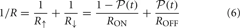 From Equations (5) and (6) the time dependence of the normalized resistance can be written as (see also supplementary online material):
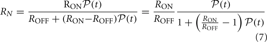 In the case of very large TER, Equation (7) simplifies to:
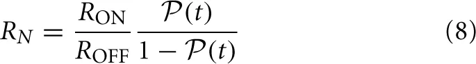 Equations (7) or (8) together with Equation (3) represent the characteristic transfer function of the ferroelectric memristor:
The experimental data can be fitted with Equation (9) in order to obtain the chatacteristic value of the switching time τ. As we know that in ultrathin epitaxial ferroelectric films the polarization switching is mostly bi-dimensional, the value of the parameter n in the above relation can be assumed to be 2, and thus one can constrain the fitting only to one parameter τ. As it can be easily seen in Figure 3C, the fit of the experimental data is very good which we interpret as the univocal result of ferroelectric domain wall kinetics. The value of the characteristic switching time is in the range of sub-μ s wich is, as expected, similar to the characteristic switching time in thin ferroelectric epitaxial PZT films of the same composition [23].
Equations (7) or (8) together with Equation (3) represent the characteristic transfer function of the ferroelectric memristor:
The experimental data can be fitted with Equation (9) in order to obtain the chatacteristic value of the switching time τ. As we know that in ultrathin epitaxial ferroelectric films the polarization switching is mostly bi-dimensional, the value of the parameter n in the above relation can be assumed to be 2, and thus one can constrain the fitting only to one parameter τ. As it can be easily seen in Figure 3C, the fit of the experimental data is very good which we interpret as the univocal result of ferroelectric domain wall kinetics. The value of the characteristic switching time is in the range of sub-μ s wich is, as expected, similar to the characteristic switching time in thin ferroelectric epitaxial PZT films of the same composition [23].
Figure 4
The analytical expression (9) can be used to predict or—better to say—to program any desired memristor state, independent from the memristor history. To show this experimentally, we analyzed the response of a ferroelectric memristor by successively applying programming pulses of constant amplitude, starting from a well-defined reference state ON, using different pulse width tA = 800 ns and tB = 1600 ns. In Figure 5, we present the time evolution of the resistance of a junction, where it can be easily seen that memristor states marked by horizontal lines can be achieved either with a long pulse tB or with a larger number of shorter pulses tA demonstrating the ability of programming any intermediate state between ROFF and RON.
Figure 5
According to the model, applying one programming pulse with the total width tt should always drive the FTJ to the same resistance as a sequence of pulses with width tf < tt of which the total time is tt = ∑ntf where n = tt/tf.
Conclusion
In summary, we have shown that a ferroelectric tunnel junction memristor based on epitaxial ferroelectric oxide ultra-thin films can be programmed in a designed way. The characteristic transfer function of this device is directly related to the polarization switching mechanism, viz. to the Kolmogorov-Avrami-Ishibashi model with two-dimensional domain growth. The characteristic transfer function of the FTJ memristor is dependent only on the characteristic switching time of the ferroelectric polarization which is in the present case of the order of 10−7 s. The physical model of MTJ-based memristors proposed above satisfies the mathematical equations describing the general features of memristors.
In comparison to other memristor devices, [3] the present device is based on a genuine electronic effect, respectively on quantum electronic transport and does not rely on ionic transport or phase change. The writing process, i.e., the partial switching of ferroelectric polarization, is achieved with rather large voltage approaching the coercive voltage of the ferroelectric layer, but still sufficiently low to comply to the nowadays microelectronic requirements. The current-based nondestructive readout, although performed at low voltages (<0.2 V) provides sufficient current density to allow downscaling and high integration density. However, further investigations have to be performed in order to identify and understand issues related to reliably, polarization back-switching, fatigue phenomena, etc.
Statements
Author contributions
Andy Quindeau, PhD student at the Max Planck Institute of Microstructure Physics. Dietrich Hesse, Professor at the Max Planck Institute of Microstructure Physics. Marin Alexe, Professor at Warwick University.
Acknowledgments
This research was financed by the German Research Foundation (DFG) via SFB762. The authors acknowledge D. Pantel and S. Götze for the TER sample.
Conflict of interest
The authors declare that the research was conducted in the absence of any commercial or financial relationships that could be construed as a potential conflict of interest.
References
1.
Di VentraMPershinY. The parallel approach. Nat Phys. (2013) 9:200–2. 10.1038/nphys2566
2.
ChuaLO. Memristor—the missing circuit element. IEEE Trans Circuit Theory (1971) 18:507–19. 10.1109/TCT.1971.1083337
3.
StrukovDSniderGSStewartDRWilliamsRS. The missing memristor found. Nature (2008) 453:80–3. 10.1038/nature06932
4.
TsymbalEYKohlstedtH. Tunneling across a ferroelectric. Science (2006) 313:181–3. 10.1126/science.1126230
5.
ChanthboualaAGarciaVCherifiROBouzehouaneKFusilSMoyaXet al. A ferroelectric memristor. Nat Maerials. (2012) 11:860–4. 10.1038/nmat3415
6.
KimDJLuHRyuSBarkC-WEomC-BTsymbalEYet al. Ferroelectric tunnel memristor. Nano Lett. (2012) 12:5697–702. 10.1021/nl302912t
7.
PantelDGoetzeSHesseDAlexeM. Reversible electrical switching of spin polarization in multiferroic tunnel junctions. Nat Mater. (2012) 11:289–93. 10.1038/nmat3254
8.
PantelDLuHGoetzeSWernerPKimDJGruvermanAet al. Tunnel electroresistance in junctions with ultrathin ferroelectric Pb(Zr0.2Ti0.8)O3 barriers. Appl Phys Lett. (2012) 100:23. 10.1063/1.4726120
9.
JiangAChenZHuiWWuDScottJF. Subpicosecond domain switching in discrete regions of Pb(Zr0.35Ti0.65)O3 thick films. Adv Funct Materials (2012) 22:2148–53. 10.1002/adfm.201102829
10.
IshibashiYTakagiY. On distribution of relaxation times in some ferroelectrics. J Phys Soc Japan (1971) 31:54–5. 10.1143/JPSJ.31.54
11.
DimmlerKParrisMButlerDEatonSPoulignyBScottJFet al. Switching kinetics in KNO3 ferroelectric thin-film memories. J Appl Phys. (1987) 61:12. 10.1063/1.338237
12.
LinesMEGlassAM. Principles and Applications of Ferroelectrics and Related Materials. Oxford: Clarendon Press1977.
13.
PantelDAlexeM. Electroresistance effects in ferroelectric tunnel barriers. Phys Rev B (2012) 82:134105. 10.1103/PhysRevB.82.134105
14.
ZhuravlevMYSabirianovRFJaswalSSTsymbalEY. Giant electroresistance in ferroelectric tunnel junctions. Phys Rev Lett. (2005) 94:246802. 10.1103/PhysRevLett.94.246802
15.
GruvermanAWuDScottJF. Piezoresponse force microscopy studies of switching behavior of ferroelectric capacitors on a 100-ns time scale. Phys Rev Lett. (2008) 100:097601. 10.1103/PhysRevLett.100.097601
16.
McQuaidRGPMcMillenMChangL-WGruvermanAGreggJM. Domain wall propagation in meso- and nanoscale ferroelectrics. J Phys Condens Matter. (2012) 24:024204. 10.1088/0953-8984/24/2/024204
17.
YangSMJoJYKimDJSungHNohTWLeeHNet al. Domain wall motion in epitaxial Pb (Zr, Ti) O 3 capacitors investigated by modified piezoresponse force microscopy. APL (2008) 92:252901. 10.1063/1.2949078
18.
GruvermanA. Nanoscale insight into the statics and dynamics of polarization behavior in thin film ferroelectric capacitors. J Mater Sci. (2009) 44:5182–8. 10.1007/s10853-009-3623-4
19.
PantelDGoetzeSHesseDAlexeM. Room-temperature ferroelectric resistive switching in Ultrathin Pb(Zr0.2Ti0.8)O3 films. ACS Nano (2011) 5:6032–8. 10.1021/nn2018528
20.
LeeDYangSMKimTHJeonBCKimYSYoonJ-Get al. Multilevel data storage memory using deterministic polarization control. Adv Materials (2012) 24:402–6. 10.1002/adma.201103679
21.
VenturaJTeixeiraJMAraujoJPSousaJB. Pinholes and temperature-dependent transport properties of MgO magnetic tunnel junctions. Phys Rev B (2008) 78:02440310.1103/PhysRevB.78.024403
22.
ShurVRumyantsevEMakarovS. Kinetics of phase transformations in real finite systems: application to switching in ferroelectrics. J Appl Phys. (1998) 84:445–51. 10.1063/1.368047
23.
LiWAlexeM. Investigation on switching kinetics in epitaxial Pb(Zr0.2Ti0.8)O3 ferroelectric thin films: role of the 90° domain walls. Appl Phys Lett. (2007) 91:26093. 10.1063/1.2825414
24.
KimDJJoJYKimYSChangYJLeeJSYoonJ-Get al. Polarization relaxation induced by a depolarization field in ultrathin ferroelectric capacitors. Phys Rev Lett. (2005) 95:237602. 10.1103/PhysRevLett.95.237602
Summary
Keywords
memristor, KAI, ferroelectric switching, ferroelectric tunnel junction, multiferroic oxides
Citation
Quindeau A, Hesse D and Alexe M (2014) Programmable ferroelectric tunnel memristor. Front. Physics 2:7. doi: 10.3389/fphy.2014.00007
Received
23 October 2013
Accepted
03 February 2014
Published
25 February 2014
Volume
2 - 2014
Edited by
Nicholas X. Fang, Massachusetts Institute of Technology, USA
Reviewed by
Byungchan Han, Daegu Gyeongbuk Institute of Science and Technology, South Korea; Pavel Lukashev, University of Nebraska - Lincoln, USA
Copyright
© 2014 Quindeau, Hesse and Alexe.
This is an open-access article distributed under the terms of the Creative Commons Attribution License (CC BY). The use, distribution or reproduction in other forums is permitted, provided the original author(s) or licensor are credited and that the original publication in this journal is cited, in accordance with accepted academic practice. No use, distribution or reproduction is permitted which does not comply with these terms.
*Correspondence: Marin Alexe, Max Planck Institute of Microstructure Physics, Weinberg 2, D-06120 Halle (Saale), Germany e-mail: malexe@mpi-halle.mpg.de
This article was submitted to Condensed Matter Physics, a section of the journal Frontiers in Physics.
Disclaimer
All claims expressed in this article are solely those of the authors and do not necessarily represent those of their affiliated organizations, or those of the publisher, the editors and the reviewers. Any product that may be evaluated in this article or claim that may be made by its manufacturer is not guaranteed or endorsed by the publisher.