 Bernhard Goll1*
 David J. Thomson2
 Lars Zimmermann3Henri Porte4
 Frederic Y. Gardes2Youfang Hu2Dieter Knoll3Stefan Lischke3Bernd Tillack3
 Graham T. Reed2Horst Zimmermann1
- 1Institute of Electrodynamics, Microwave and Circuit Engineering (EMCE), Vienna University of Technology, Vienna, Austria
- 2Optoelectronics Research Centre (ORC), University of Southampton, Southampton, UK
- 3IHP, Im Technologiepark, Frankfurt (Oder), Germany
- 4Photline Technologies, Besancon, France
This paper presents as a novelty a fully monolithically integrated 10 Gb/s silicon modulator consisting of an electrical driver plus optical phase modulator in 0.25 μm SiGe:C BiCMOS technology on one chip, where instead of a SOI CMOS process (only MOS transistors) a SiGe BiCMOS process (MOS transistors and fast SiGe bipolar transistors) is implemented. The fastest bipolar transistors in the BiCMOS product line used have a transit frequency of ft ≈ 120 GHz and a collector-emitter breakdown voltage of BVCE0 = 2.2 V (IHP SG25H3). The main focus of this paper will be given to the electronic drivers, where two driver variants are implemented in the test chips. Circuit descriptions and simulations, which treat the influences of noise and bond wires, are presented. Measurements at separate test chips for the drivers show that the integrated driver variant one has a low power consumption in the range of 0.66 to 0.68 W but a high gain of S21 = 37 dB. From the large signal point of view this driver delivers an inverted as well as a non-inverted output data signal between 0 and 2.5 V (5 Vpp differential). Driver variant one is supplied with 2.5 V and with 3.5 V. Bit-error-ratio (BER) measurements resulted in a BER better than 10−12 for voltage differences of the input data stream down to 50 mVpp. Driver variant two, which is an adapted version of driver variant one, is supplied with 2.5 and 4.2 V, consumes 0.83 to 0.87 W, delivers a differential data signal with 5.6 Vpp at the output and has a gain of S21 = 40 dB. The chip of the fully integrated modulator occupies an area of 12.3 mm2 due to the photonic components. Measurements with a 240 mVpp electrical input data stream, 1.25 V input common-mode voltage and for an optical input wavelength of 1540 nm resulted in an extinction ratio of 3.3 dB for 1 mm long RF phase shifters in each modulator arm driven by driver variant one and a DC tuning voltage of 1.2 V. The extinction ratio was 8.4 dB at a DC tuning voltage of 7 V for a device with 2 mm long RF phase shifters in each arm and driver variant two.
Introduction
Data rates of 10 Gb/s (e.g., ethernet standard) for optical transmission is a well-established technology and multichannel transmission systems have been demonstrated [1]. The first combination of SOI CMOS electronics with silicon photonics can be found in Narasimha et al. [2] and Bruckwalter et al. [3], where a fully integrated 4 × 10 Gb/s dense wavelength division multiplex (DWDM) optoelectronic transceiver with Mach–Zehnder modulators and a fully integrated 25 Gb/s transceiver with photonic microring resonator modulators in 0.13 μm SOI CMOS are presented, respectively. With the same architecture of Narasimha et al. [2] Luxtera presented a monolithically integrated 4 × 25 Gb/s transceiver in 0.13 μm SOI CMOS in Pinguet et al. [4].
This paper presents as a novelty a fully monolithically integrated 10 Gb/s silicon modulator consisting of an electrical driver plus optical phase modulator in 0.25 μm SiGe:C BiCMOS technology on one chip, where instead of a SOI CMOS process (only MOS transistors) a SiGe BiCMOS process (MOS transistors and fast SiGe bipolar transistors) is implemented. The fastest bipolar transistors in the BiCMOS product line used have a transit frequency of ft ≈ 120 GHz and a collector-emitter breakdown voltage of BVCE0 = 2.2 V (IHP SG25H3). In general with bipolar transistors a higher gain can be achieved than with CMOS transistors because of the exponential dependence of the collector current on the base-emitter voltage in contrast to the quadratic dependence of the drain current on the gate-source voltage in the case of a MOSFET. Hence a higher gain can be achieved in a bipolar amplifier with less amplifier stages by trend. The main focus of this paper will be given to the electronic drivers. Two driver variants, which have been implemented into test chips, are described. Driver variant one not co-integrated together with a Mach-Zehnder modulator is already described in Goll and Zimmermann [5]. In contrast to Goll and Zimmermann [5], a second driver (driver variant two) and simulations of eye diagrams, which treat the influences of noise and bond wires on the drivers' performance as well as more measured eye diagrams of the fully integrated modulator chips than depicted in Thomson et al. [6] are presented. Driver variant two is designed in such a way that the collector-emitter voltages of the fast transistors in the last stage are close to breakdown. Hence an output voltage difference of 5.6 Vpp has been achieved.
Overview, Optical Modulator, and Process Flow
An overview of the modulator chip including a cross section of the diode used for phase modulation in a Mach–Zehnder interferometer in dual-drive configuration is depicted in Figure 1. The phase shifters in the interferometer arms are based upon carrier depletion in a reverse biased pn junction which is integrated with an SOI rib-waveguide. The waveguide is of dimensions 220 nm in height, 400 nm rib width and 100 nm slab height [6, 7]. The pn junction is located at the edge of the waveguide rib, where the p-region is doped with a lower concentration than the n-region. Hence with a bias voltage applied for reverse operation of the diode the depletion region extends into the optical waveguide rib. The electrical contacts to the metal layers are built by highly doped n+ and p+ regions in the slab, which are located 600 and 500 nm away from the left and right edge of the rib, respectively. DC tuning sections (2.55 mm length, folded to save chip area, controlled with voltage VDC), which use the same pn junction as the high-speed modulation part but with larger separation of the n+ and p+ doped regions from the waveguide, are included in both interferometer arms as depicted in Figure 1 to allow the operating point to be adjusted electrically. The optical modulator has a phase efficiency of approximately 2.3 Vcm for the voltage range delivered by the driver. The loss of a phase shifter in a modulator arm is 3.6 dB/mm for the light and the −6 dB cut-off frequency of a 2 mm long modulator electrode amounted to 10 GHz (S21 parameter measurement). So the optical modulator is sufficient for 10 Gb/s operation. The block on the lower left in Figure 1 illustrates the electronic driver, which provides a differential output data stream (OUT+ and OUT−) to drive the electrodes of the phase shifting elements in both arms of the modulator. Hence the resulting differential voltage for modulation switches between 0 V and 2 × Vd.
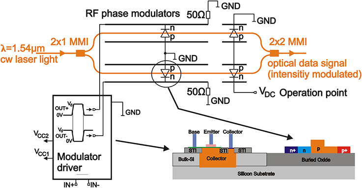
Figure 1. Overview of the fully integrated modulator: A modulator driver drives the electrodes of a Mach–Zehnder modulator in dual-drive configuration. The functional cross-sections of the phase-shifting diode in the photonic part and of a bipolar transistor in the electronic part are shown in the lower right.
To combine silicon photonic elements with the standard IHP SG25H3 BiCMOS process (see Figure 2), the process flow has been adapted to combine local-SOI areas with bulk-Si areas [8]. The starting substrate is photonic SOI, which is etched down to the handling wafer in the circuit part of the complete photonic-electronic integrated chip and then locally regrown by Si-epitaxy. After polishing to obtain surfaces at the same height for local-SOI and for bulk silicon, the BiCMOS process follows a modified flow, where at specific points additional photonic process modules are inserted. After local SOI fabrication and nanowaveguide structuring (1st photonic module) a standard BiCMOS process flow follows with several process steps for hetero-junction bipolar transistors. The second photonic module is the front-end structure of the silicon photonic modulator, which consist of the ion implantation steps and an intermediate waveguide etch for a 100 nm slab height. There source/drain implantations, which are used e.g., for the modulator's contacts and the application of a silicide blocking layer is implemented. In the third photonic module shallow trenches are etched in the top-Si layer of the SOI regions to create optical waveguide and grating coupler structures. The following process steps until completion are patterning of the silicide blocking masks, Source/Drain annealing, cobalt salicidation, a local interconnect process and adding contacts plus five metal layers up to the pads including a final passivation layer.
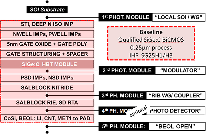
Figure 2. Process flow.
Circuit Description of Drivers
Two variants of electric drivers are designed for an implementation to the modulator chip. Both drivers consist of the same pre-amplifier, which processes the input data signal. The pre-amplifier is followed by the output stage, which consists of a level shifter and some amplifier to reach the full voltage swing for driving the modulators at 10 Gb/s. Driver variant one differs from driver variant two in the output stage, where small changes in the schematic create a differential output voltage of 5.6 Vpp at 4.2 V power supply (variant two) instead of 5 Vpp at 3.5 V power supply (variant one).
Pre-Amplifier
The schematic of the pre-amplifier is depicted in Figure 3. The supply voltage amounts to VCC1 = 2.5 V. After applying an input data stream to nodes IN+/IN−, where 50 Ω resistors ensure a matching to an external 50 Ω system, a first amplification of the differential input data stream is performed with a differential amplifier consisting of transistors TCS1, T1, and T2 and resistors R1 and R2. The main problem in designing a fast driver with a large output voltage difference is the small collector-emitter breakdown voltage (BVCE0 = 2.2 V) of the fast bipolar transistors with ft ≈ 120 GHz. Therefore, in the pre-amplifier an appropriate operating point is set with the help of a common-mode feedback circuit (CMFB) if the common-mode voltage of the input data stream varies. The common-mode voltage (node CM) at nodes OT1+/OT1− is measured with the help of two equal resistors R3 and R4, compared with an reference voltage REFCM = 1.8 V and regulated via an integrator (operational amplifier OPA1 with capacitors C13 and C14) and transistor MP1 to 1.8 V. OPA1 is a Miller-compensated operational amplifier with 39 dB DC gain and a −3 dB cut-off frequency of 18 MHz. The time constant of the CMFB is around 130 ns, which is sufficient that up to 1000 bits with the same logical value can follow each other. Another implementation to exclude collector–emitter voltages larger than BVCE0 = 2.2 V is the automatic gain control (AGC). If the voltage difference of the input data stream exceeds 100 mVpp, then the AGC starts to reduce the amplification of the pre-amplifier. This is done with the help of an amplifier with peak detector, which measures the peak voltage difference at nodes OT1+/OT1−, compares it with a reference voltage REFAGC and generates a control voltage VAGC for adding an additional current to the current mirror T21 to TCS1 to increase the amplification. For a small voltage difference at OT1+/OT1− the drain current of MP2 is at its maximum thus having the maximum voltage amplification of 21 dB. If MP2 is turned off IDC defines a minimum voltage gain of nominal 16 dB. The settling time of the AGC for an error lower than 1% of the final value is 1.55 μs according to simulations.
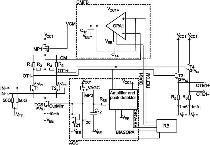
Figure 3. Schematic of the pre-amplifier of modulator driver variant one and variant two (AGC, Automatic Gain Control; CMFB, Common-Mode Feedback). The emitter areas are AE1 = 0.353 μm2 and AE2 = 0.493 μm2.
Reference voltages and bias currents are created in a circuit block, called here the reference block (RB). It consists of a simple bandgap reference voltage source with 1.123 V at 25°C according to nominal simulations. When changing only the temperature in simulation with nominal device parameters this voltage varied at maximum by 15 mV in a range of 0 to 100°C. The result of a Monte-Carlo simulation considering the complete process variation range with 100 samples at 40°C was a mean voltage of 1.125 V with 8.9 mV standard deviation.
The gain-regulated and common-mode voltage regulated differential data signal OT1+/OT1− is level-shifted and buffered by emitter followers, which consist of transistors T3, T4 as well as resistors R5 and R6, respectively. The resulting differential data stream OTE1+/OTE1− is applied to the level shifter in the adjacent output stage. The bipolar transistors T3 and T4 have a smaller transit frequency of 45 GHz but a higher collector-emitter breakdown voltage of approximately BVCE0 ≈ 5 V, which is larger than the supply voltage (VCC1 = 2.5 V), because an emitter follower has a voltage gain of one and hence does not need the fastest transistors available.
Output Stage
The differential data signal of the preceding pre-amplifier (OTE1+/OTE1−) is applied to the level shifter at the beginning in the output stage. The circuit of the output stage is depicted in Figure 4. Modulator driver variant one differs from driver variant two in the schematic of the output stage. All black drawn electric components in Figure 4 refer to driver variant one. Driver variant two consists of the black drawn components and additional the gray drawn electronic parts in Figure 4. The level shifter at the input of the driver stage is supplied with VCC1 = 2.5 V and provides two voltage level shifted differential data signals (nodes INT1+/INT1+ and nodes INT2+/INT2−) for the following circuit stages, which are supplied with higher supply voltages VCC2 = 3.5 V (driver variant one) and VCC2 = 4.2 V (driver variant two). The level shifting is performed for signals INT1+/INT1− by the voltage divider R7, R9 for INT1+ and the equal divider R8, R10 for INT1−. A second level shifting is done with emitter followers T7, R11 and T8, R12 for signals INT2+ and INT2−, respectively. With these two level shifted differential data signals INT1+/INT1− and INT2+/INT2−, which are applied to the bases of transistors T12/T11 and T10/T9, respectively, the voltages at nodes AP+ as well as AP− are subdivided to the collector-emitter voltage drop of two bipolar transistors and a resistor in series, e.g., the voltage level at AP+ is the sum of the collector-emitter voltages of T9 and T11 and a small voltage drop at resistor R13. Hence the fast transistors T11 and T12 act as driven cascode transistors, with which the voltage levels at nodes AP+ and AP− can reach higher levels than the collector-emitter breakdown voltage limit of a single fast transistor (BVCE0 ≈ 2.2 V) while the collector-emitter voltage of e.g., T9 and T11 (AP+) will not reach the breakdown voltage. Current source MN1 is biased with the RB with reference voltage BIAS1 and capacitors C1 and C2 are added to avoid peaks in the collector-emitter voltage of T5 and T6. As a trade-off these capacitors cause a slight decrease of bandwidth. Transistors T7 and T8 of the emitter follower are slower (ft ≈ 45 GHz) but have a higher collector-emitter breakdown voltage (BVCE0 ≈ 5 V). To enhance the bandwidth for signals AP+/AP−, capacitor C4 = 2 pF has been added. In contrary to C4, capacitor C3 somewhat slows down the nodes at the emitters of T11 and T12. This reduces peaks of the collector-emitter voltages, which occur due to different slew rates of e.g., at node AP+ and the emitter of T11. The differential data signal of AP+/AP− is applied to a passive network, which controls the base potentials of transistors T17 and T18 on the one hand and level-shifted via emitter followers T13, R17, R19, C5 and T14, R18, R20, C6 on the other hand. Resistors R17, R19 as well as resistors R18 and R20 are for fine-adjustment of the common-mode voltage level of the differential data signal at APD+/APD− and capacitors C5 = C6 = 800 fF increase the bandwidth. Again transistors T13 and T14 are slower but have a higher collector-emitter breakdown voltage. The data stream of APD+/APD− is amplified by transistors T15 and T16, where capacitors C7 and C8 (both 200 fF) decrease the rise- and fall-time at nodes AP2+ and AP2− to suppress voltage peaks in the collector-emitter voltage of T17 and T18, respectively. Capacitors C7 and C8 are too small to cause instabilities due to positive feedback. The passive network is implemented to control the base potentials API− and API+ of transistors T17 and T18, respectively, to get again a division of the voltage of e.g., AP2+ to the collector-emitter voltages of transistors T17 and T18 to overcome the collector-emitter breakdown limit. An advantage of the passive network is, that an additional amplifier stage to drive the bases of transistors T17 and T18 is omitted, which saves power. Capacitors C9, C10, C11, and C11B (driver variant two) are implemented to get a better dynamic behavior. The amplified differential data signal AP2+/AP2− is buffered by emitter follower transistors T19 and T20, which drive the modulator electrodes and the load of 50 Ω. T19 and T20 have a smaller transit frequency (45 GHz) but a higher collector-emitter breakdown voltage (BVCE0 ≈ 5 V).
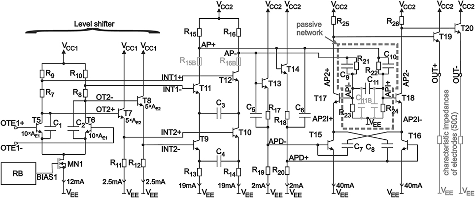
Figure 4. Schematic of the output stages of the modulator drivers: The black drawn electrical components alone are the schematic of driver variant one. The black components including the light gray drawn components are the schematic of driver variant two.
For illustration in Figure 5 transient simulations of the last amplifier in the output stage are shown. The left side contains the transient results for driver variant one (VCC2 = 3.5 V) and on the right side the results for driver variant two (VCC2 = 4.2 V) are shown. For driver variant one it can be seen that the collector-emitter voltages of transistors T17 (AP2+–AP2I+) and T15 (AP2I+) are smaller than 2.1 V and smaller than 1.7 V, respectively. This is below the limit of the collector-emitter breakdown voltage of BVCE0 = 2.2 V. On the right side of Figure 5 for driver variant two the collector-emitter voltage of transistor T15 exceeds the limit by 0.1 V. This can be tolerated because the breakdown limit BVCE0 is defined for an ideal current source, which forces the base current of T15. In reality the resistance, seen from the base of T15 toward the back circuitry is smaller than infinity, which extends the collector-emitter breakdown limit BVCE0 to somewhat higher voltage values [9].
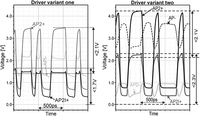
Figure 5. Transient simulations of the final amplifier in the output stage. The signals for driver variant one can be found on the left side and the transients for driver variant two are depicted on the right side.
The data signal at OUT+ and OUT− is similar to the data signal AP2+ and AP2− but with the exception that due to the level shifting of transistors T19 and T20 the voltage levels for OUT+ as well as OUT− correspond to 0 V and 2.5 V for driver variant one and 0 V and 2.8 V for driver variant two. This results in differential output data signals with 5 Vpp for driver variant one and 5.6 Vpp for driver variant two.
Results
A test chip for driver variant one as well as for driver variant two has been designed and produced in IHP SG25H3 technology. The layout plots and chip photos can be seen in Figure 6. The chip size amounts to 0.54 mm2.
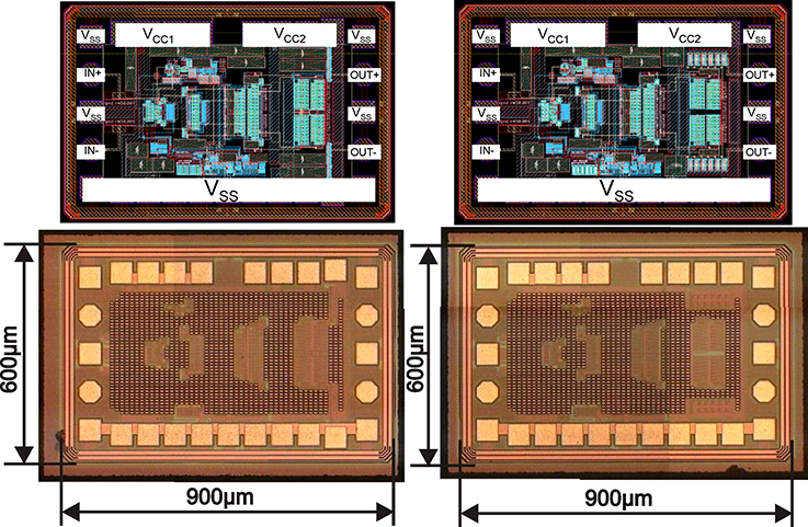
Figure 6. Layout plots (top) and chip photos (bottom) of the realized test chips of both driver variants. The pictures on the left side correspond to driver variant one and that on the right side correspond to driver variant two.
The function of the chip may be influenced by the inductances of the bond wires, with which the pads are connected to the PCB. For a rough estimation the inductance amounts to 1 nH per 1 mm bond-wire length. Figure 7 shows the added inductances for circuit simulation, where now between chip ground (VSS) and PCB ground (GND) has to be distinguished. To reduce the amount of inductance, bond wires in parallel were bonded from the pads to GND. A rough estimation are the values LI = LO = 600 pH for the bond inductance between PCB and the input pad or output pad, L1 = L2 = 400 pH are in series to the power supply pads VCC1 and VCC2 and LG = 200 pH corresponds to the overall inductance from VSS to GND. For the eye diagram simulations, the bond wires have been included.
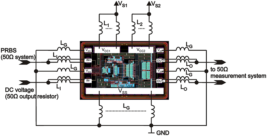
Figure 7. Inductances caused by bond wires. VS1 and VS2 are supply voltage nodes on the PCB, GND is the PCB ground potential.
Figure 8 shows the simulated differential output voltage noise spectrum in V/√Hz of driver variant one and driver variant two excluding bond wires. For the sake of completeness the input referred voltage noise spectrum for node IN+ is added. These simulations correspond only to the noise generated by the drivers themselves. The simulated output referred rms voltage is nearly equal for both drivers and amounts to 129 mV. In reality the noise of the data source, supply noise, coupling effects and substrate noise raise the effective noise rms voltage.
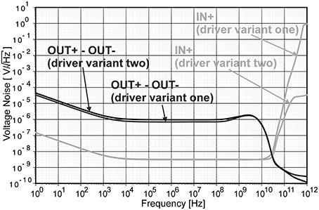
Figure 8. Simulated voltage noise spectrum in V/√Hz for the output difference voltage OUT+ – OUT− and for input node IN+ for both driver variants.
The simulated eye diagrams at 10 Gb/s for 50 mVpp differential input voltage of driver variant one including noise and bond wire inductances are shown in the upper area of Figure 9.
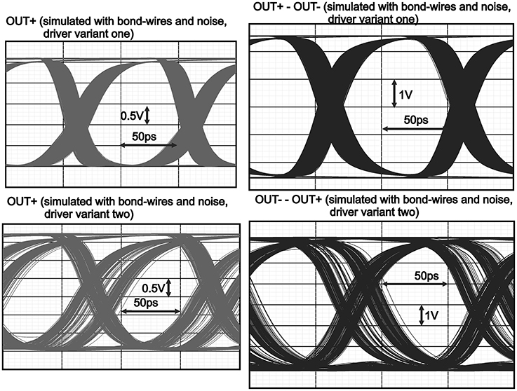
Figure 9. Simulated eye diagrams for driver variant one (top) and driver variant two (bottom) for 50 mVpp differential input voltage at 10 Gb/s including the influence of bond-wires and noise. The eye diagram of driver variant two is degraded by a not optimized capacitor C4 = 2 pF (see Figure 4).
Eye diagram measurements of the fabricated test chips of driver variant one and driver variant two have been done with the chip glued and bonded onto a PCB, on which 50 Ω microstrip transmission lines were lead as near as possible to the high frequency pads. To IN+ a 10 Gb/s pseudo-random-bit-sequence PRBS 231-1 with a DC bias of 1.25 V and at IN- a reference voltage of 1.25 V from a voltage source with 50 Ω output resistance have been applied. The supply voltages are 2.5 V and 3.5 V for driver variant one and 2.5 V and 4.2 V for driver variant two. The measured eye diagrams for a 100 mVpp data signal at the input for driver variant one are shown on the left side in Figure 10 and the measured eye diagram for driver variant two can be seen depicted on the right side of Figure 10. Driver variant one has a pretty and open eye diagram, but driver variant two shows some data dependent jitter. Simulations have shown that this jitter can be improved in optimizing the value of capacitor C4 in Figure 4 to lower values (see Figure 11). The load of the bases of transistors T19 and T20 on AP2+ and AP2– causes a slight ramp in the roof of the measured eye diagrams. The large signal swing in opposite to a small-signal consideration could also be the reason for more noise degradation of the eye-diagram. So for a sequence of equal bits, it can be said that temporarily another operating point becomes valid, where the noise performance or bandwidth may change.
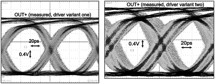
Figure 10. Measured eye diagrams at 10 Gb/s for 100 mVpp input voltage difference of driver variant one (left side) and driver variant two (right side).
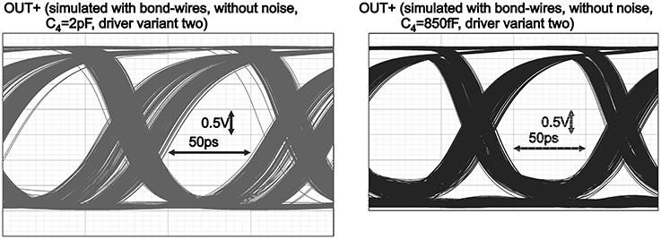
Figure 11. Simulated eye diagrams, which includes the influence of bond wires: Reducing capacitor C4 from 2 pF down to 850 fF improves the eye diagram.
Bit-error-ratio (BER) measurements resulted in a BER < 10−12 for input voltage differences down to 40 mVpp for driver variant one and down to 50 mVpp for driver variant two. The power consumption of a chip of driver one characterized electrically alone (without integrated modulator) amounted to 0.68 W and a chip of driver two consumed 0.87 W. These power values include transistors T19 and T20 with their 50 Ω loads, but exclude the 50 Ω matching resistors at input nodes IN+/IN−.
AC measurements have been done with the help of a wafer prober, a network analyzer and high-frequency Z-probes. By using a standard substrate for calibration the S-parameter measurement resulted in S21 = 37 dB with a −3 dB cut-off frequency of 7.1 GHz for driver variant one and S21 = 40 dB with 7.5 GHz cut-off frequency for driver variant two. S11 was below −9 dB in the transmission band.
Fully Integrated Modulator Chip
In using the process flow of Figure 2 fully integrated modulator chips have been fabricated, where the block diagram is depicted in Figure 1. The chip photo of a modulator driver with a 2 mm long optic modulator device is shown on the top of Figure 12 and the corresponding layout plot is depicted at the bottom. It should be mentioned that the area of the photonic components could be reduced when optical input and output structures would be placed at one side and the lengths of the optical waveguides leading to them would be reduced. It also can be seen, that the area at the right of the electronic driver can be used for additional circuits.
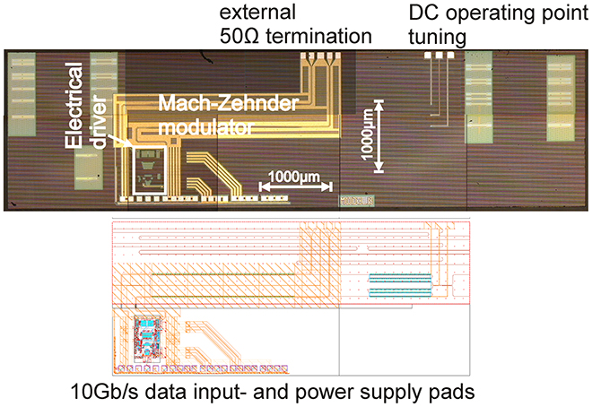
Figure 12. Chip photo (top) and layout plot (bottom) of a fully integrated modulator with electronic driver and a 2 mm optical modulator device.
Measurements have been performed at an optical input wavelength of 1540 nm, which was coupled in via a grating coupler to the monolithically integrated modulator. The electrical supply voltages, RF input signals, bias voltages and the connections for the 50,Ω termination of the electrodes were applied with RF probe tips and probe needles to the pads of the modulator chip. The test of the fully integrated modulator has been done by applying a PRBS 27-1 data stream with 240 mVpp to the inputs of the driver, where the common-mode voltage level at the input amounted to 1.25 V. An Erbium Doped Fiber Amplifier (EDFA) has been used to boost the signal and an optical band-pass filter has been connected before the light is passed to a digital communication analyzer for measurement to reduce noise from neighboring wavelengths. The resulting optical eye diagrams for a wavelength of 1540 nm can be seen in Figure 13. On the left side of Figure 13, the results of a device with 1 mm long RF phase shifters in each modulator arm and driver variant one (VCC1 = 2.5 V, VCC2 = 3.5 V) are depicted. There an extinction ratio of 3.3 dB at a DC tuning voltage VDC = 1.2 V at 10 Gb/s and 5.1 dB extinction ratio (VDC = 1.2 V) at 5 Gb/s have been reached. On the right side of Figure 13 the eye diagrams for the device with 2 mm long RF phase shifters in each modulator arm with driver variant two (VCC1 = 2.5 V, VCC2 = 4.2 V) are shown. There extinction ratios of 8.4 dB at VDC = 7 V at 10 Gb/s data rate and 8 dB (VDC = 6 V) at 5 Gb/s have been measured. The noise power, which was generated by the EDFA and which amounted to 0.24 mW, has been subtracted from the logical high and low levels to calculate the experimental extinction ratios. A BER measurement would not give correct results because there was too much coupling loss from the fiber to the chip as well as the used EDFA added a considerable amount of noise. The main contributions of the on-chip optical losses are: phase shifter (3.6 dB/mm), tuning section (3.6 dB), 2 × 2 multimode interference coupler (MMI) combining (0.7 dB), and passive waveguide loss (0.8 dB). The measured overall electrical power consumption of the 1 mm modulator with driver variant one is 0.66 W and of the 2 mm modulator with driver variant two is 0.83 W.
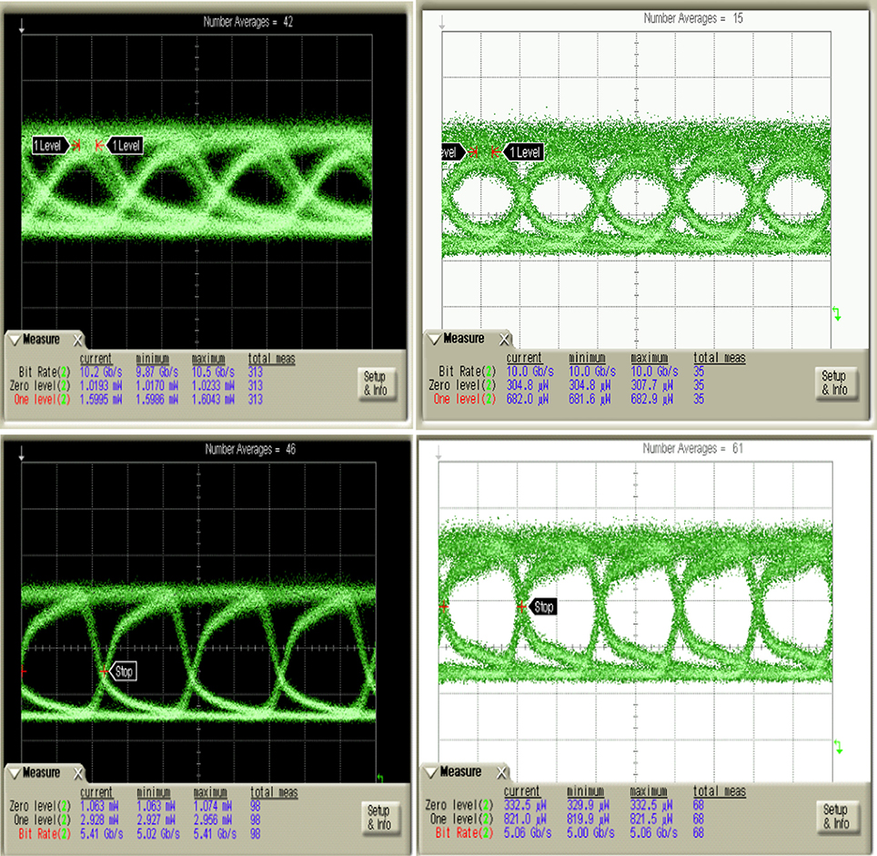
Figure 13. Measurement results of the fully integrated modulator: The optical eye diagrams of the fully integrated optical modulator at 10 Gb/s (top) and 5 Gb/s (bottom) data rate (PRBS data stream with 240 mVpp at the input of the driver) are shown on the left for a chip with driver variant one and a 1 mm long modulator and on the right for a chip with driver variant two combined with a 2 mm long modulator.
Comparison and Conclusion
Two variants of electrical modulator drivers, which are produced in a 0.25 μm SiGe:C 120 GHz-BiCMOS process (IHP SG25H3) are presented. They differ from each other in some capacitances, some resistors, in their supply voltage of the output stage and in their output voltage difference (5 Vpp for variant one and 5.6 Vpp for variant two when applying a 100 mVppdifferential data signal at the inputs). The comparable large amplification makes it possible that these drivers are capable to treat LVDS and CML logical standard voltage levels at the input. The driver variants have been designed for operating at 10 Gb/s data rate with a high gain of S21 = 37 dB and S21 = 40 dB but with a low power consumption of 0.68 W and 0.87 W.
In order to compare the suggested photonic-electronically integrated modulators to the state of the art, we give a short overview of the literature. In [2], a 10 Gb/s modulator driver for 2 × 50 Ω load in 0.13 μm SOI CMOS is reported, where with inductive shunt peaking in every stage, a 50 mVpp data signal is amplified to 5 Vpp. This driver consumed 575 mW. The functionality of the driver has been proven as part in a whole transceiver, but not with a separate test chip. In general implementing inductances in integrated circuits consumes much chip area. To compare the modulator drivers directly at 10 Gb/s in a similar process in Li and Tsai [10] a 10 Gb/s driver in 0.35 μm SiGe BiCMOS consuming 0.56 mm2 chip area with 0.8 W power consumption, where a 500 mVpp data signal is amplified to 9 Vpp was presented. In Mandegaran et al. [11] a 10 Gb/s driver in 0.18 μm SiGe BiCMOS technology is presented, which consumed 1.2 mm2 chip area and 3.7 W power and which at a 500 mVppdata signal (250 mV on each input) reached 8 Vpp at the output. The driver for the active microring resonator in Bruckwalter et al. [3] with a load capacitance of only 50 fF consumes less power and therefore less chip area than the driver for a Mach-Zehnder modulator in dual-drive configuration (typical length of 2–3 mm of electrodes), where two times the termination of an electrode line (50 Ω) and additionally the capacitances of the diodes in reverse operation have to be driven. A Mach-Zehnder modulator in dual-drive configuration compared to a microring resonator has the advantages of an operation with a very low chirp [6], more than a factor of 100 higher optical bandwidth and lower sensitivity to process tolerances and temperature [12].
Two fully integrated modulators combining SOI silicon photonics with electrical bulk silicon in 0.25 μm SiGe BiCMOS are presented. To the author's knowledge, this is the first monolithic photonic integration in the electronic frontend of a high-performance BiCMOS technology compared to 0.13 μm SOI CMOS used in Narasimha et al. [2] and Bruckwalter et al. [3]. A maximum data rate of 10 Gb/s of the fully integrated modulator devices (Mach–Zehnder modulator in dual-drive configuration) has been demonstrated. The combination of driver variant one with a 1 mm long optical modulator has reached an extinction ratio of 3.3 dB at 10 Gb/s and 5.1 dB at 5 Gb/s while consuming 0.66 W. The fully integrated modulator containing driver variant two with a 2 mm long optical modulator consumed 0.83 W power and extinction ratios of 8.2 dB at 10 Gb/s and 8 dB at 5 Gb/s have been measured. It should be noted that faster SiGe BiCMOS modulators up to 40 Gb/s can be realized if instead of SG25H3 the similar process line SG25H1 with its faster bipolar transistors (up to ft = 200 GHz) is used for the driver design. The higher gain of bipolar transistors compared to MOSFETs is a further advantage compared to a typically slower CMOS process described in [2]. The advantage of bipolar transistors compared to typically slower CMOS transistors is a higher gain-bandwidth product. Mach–Zehnder modulators operating up to 40 Gb/s without electrical drivers have been already demonstrated in [7].
Conflict of Interest Statement
The authors declare that the research was conducted in the absence of any commercial or financial relationships that could be construed as a potential conflict of interest.
Acknowledgments
The authors acknowledge funding in the European project HELIOS (FP7-224312) and by an EPSRC funded project in the UK, “Silicon Photonics for Future Systems.”
References
1. Kuchta DM, Kwark YH, Schuster C, Baks C, Haymes C, Schaub J, et al. 120-Gb/s VCSEL-based parallel-optical interconnect and custom 120-Gb/s testing station. IEEE J Lightwave Technol. (2004) 22:2200–12. doi: 10.1109/JLT.2004.833255
2. Narasimha A, Analui B, Yi L, Sleboda TJ, Abdalla S, Balmater E, et al. A fully integrated 4 × 10-Gb/s DWDM optoelectronic trasceiver implemented in a standard 0.13 μm CMOS SOI technology. IEEE J Solid-St Circ. (2007) 42:2736–44. doi: 10.1109/JSSC.2007.908713
3. Bruckwalter JF, Zheng, X, Guoliang L, Raj K, Krishnamoorthy AV. A monolithic 25-Gb/s transceiver with photonic ring modulators and Ge detectors in a 130-nm CMOS SOI process. IEEE J Solid-St Circ. (2012) 47:1309–22. doi: 10.1109/JSSC.2012.2189835
Pubmed Abstract | Pubmed Full Text | CrossRef Full Text | Google Scholar
4. Pinguet T, De Dobbelaere PM, Foltz D, Gloeckner S, Hovey S, Liang Y, et al. “25 Gb/s silicon photonic transceivers,” In: IEEE 9th International Conference on Group IV Photonics (GFP). (2012). (San Diego, CA), pp. 189–91. doi: 10.1109/GROUP4.2012.6324129
5. Goll B, Zimmermann H. A 10 Gb/s 0.25 μm SiGe modulator driver for photonic-integration. Analog Integr Circ Signal Process. (2014) 79:15–25. doi: 10.1007/s10470-013-0235-3
6. Thomson DJ, Porte H, Goll B, Knoll D, Lischke S, Gardes FY, et al. Silicon carrier depletion modulator with 10 Gbit/s driver realized in high-performance photonic BiCMOS. Laser Photonics Rev. (2013) 8:180–7. doi: 10.1002/lpor.201300116
7. Thomson DJ, Gardes FY, Sheng Liu, Porte H, Zimmermann L, Fedeli J-M, et al. High performance Mach Zehnder based silicon optical modulators. IEEE J Sel Top Quantum Electron. (2013) 19:3400510. doi: 10.1109/JSTQE.2013.2264799
8. Zimmermann L, Thomson DJ, Goll B, Knoll D, Lischke S, Gardes FY, et al. “Monolithically integrated 10Gbit/sec silicon modulator with driver in 0.25μm SiGe:C BiCMOS,” in 39th European Conference and Exhibition on Optical Communication (ECOC) (2013). (London, UK), p. 1–3. doi: 10.1048/cp.2013.1441
9. Freeman G, Meghelli M, Kwark Y, Zier S, Rylyakov A, Sorna MA, et al. 40-Gb/s circuits built from a 120-GHz fT SiGe technology. IEEE J Solid-St Circ. (2002) 37:1106–14. doi: 10.1109/JSSC.2002.801170
10. Li D-U, Tsai C-M. 10-Gb/s modulator drivers with local feedback networks. IEEE J Solid-St Circ. (2006) 41:1025–30. doi: 10.1109/JSSC.2006.872878
11. Mandegaran S, Hajimiri A. A breakdown voltage multiplier for high voltage swing drivers. IEEE J Solid-St Circ. (2007) 42:302–12. doi: 10.1109/JSSC.2006.889390
Keywords: 10 Gb/s, electro-optic modulator, modulator driver, monolithically integrated modulator, 0.25 μm SiGe:C BiCMOS
Citation: Goll B, Thomson DJ, Zimmermann L, Porte H, Gardes FY, Hu Y, Knoll D, Lischke S, Tillack B, Reed GT and Zimmermann H (2014) A monolithically integrated silicon modulator with a 10 Gb/s 5 Vpp or 5.6 Vpp driver in 0.25 μm SiGe:C BiCMOS. Front. Phys. 2:62. doi: 10.3389/fphy.2014.00062
Received: 05 September 2014; Paper pending published: 25 September 2014;
Accepted: 17 October 2014; Published online: 07 November 2014.
Edited by:
Kensuke Ogawa, Fujikura Ltd., JapanCopyright © 2014 Goll, Thomson, Zimmermann, Porte, Gardes, Hu, Knoll, Lischke, Tillack, Reed and Zimmermann. This is an open-access article distributed under the terms of the Creative Commons Attribution License (CC BY). The use, distribution or reproduction in other forums is permitted, provided the original author(s) or licensor are credited and that the original publication in this journal is cited, in accordance with accepted academic practice. No use, distribution or reproduction is permitted which does not comply with these terms.
*Correspondence: Bernhard Goll, Institute of Electrodynamics, Microwave and Circuit Engineering (EMCE), Vienna University of Technology, Gusshausstrasse 25/354, 1040 Vienna, Austria e-mail:YmVybmhhcmQuZ29sbEB0dXdpZW4uYWMuYXQ=