 Chen Li
 Zhiting Tian*
- Sibley School of Mechanical and Aerospace Engineering, Cornell University, Ithaca, NY, United States
Nanostructured materials are of great interest for many applications because of their special properties. Understanding the effect of grain boundaries on phonon transport in polycrystals is important for engineering nanomaterials with desired thermal transport properties. The phonon transport properties of Σ3 grain boundaries in silicon are investigated by employing atomistic Green's function method. Results show that similar to electron transport, the perfect grain boundary does not significantly reduce the thermal conductance, while defective grain boundaries can dramatically reduce the thermal conductance. This work may be helpful for the understanding of the underlying thermal transport mechanism across grain boundaries and the design of grain boundaries for energy applications.
Introduction
Nanostructured materials are promising and attracting considerable attention because they are the fundamental building blocks for continuous technology advancement and have special properties due to the nanoscale size [1]. Polycrystals widely exist in nanostructured materials while single-crystals only form in special conditions. Polycrystals are comprised of many individual grains and grain boundaries are the interfaces between different grains. Understanding the effect of grain boundaries is critical in controlling transport properties. For electron transport, the effects of grain boundaries on electron mobility has been studied both experimentally [2–4] and theoretically [5–7]. Grain boundaries generally present an energy barrier to the transport of electrons and lead to a reduction of electron mobility [2, 4]. However, perfect (defect-free) grain boundaries were found to be almost transparent to electron transport in highly symmetric grain boundaries [8].
Besides electron transport, grain boundaries in polycrystals play an important role in thermal transport [9–12] because grain sizes are usually nanometers or sub-microns, which are comparable to phonon mean free paths. The thermal conductivity of polycrystals is lower than that of their corresponding single-crystals and further reduces with decreasing grain sizes due to the decreased phonon mean free paths [1, 13–15]. The overall thermal conductivity reduction has been observed in polycrystals of a wide variety of materials [16–19], which has been attributed to many mechanisms including the effects of grain boundaries, vacancies, impurities, and dislocations [1, 20–22]. Understanding the effect of grain boundaries on phonon transport is important and necessary for the engineering and design of nanomaterial thermal transport properties for many applications such as thermoelectrics [23, 24], micro/nano-electromechanical devices [25], phononic devices [26], and thermal barrier coatings [17].
Non-equilibrium molecular dynamics were previously performed to calculate the thermal interface conductance across grain boundaries, while phonon wave packets were launched in molecular dynamics to study the phonon transmission across grain boundaries [27–29], which can calculate the mode-dependent transmission. Atomistic Green's function method [30, 31], a computationally efficient way to extract frequency-dependent phonon transmission in a single calculation, has been applied to study phonon transport across interfaces [32–35] but has not yet been applied to study phonon transport across grain boundaries. Moreover, the effects of perfect vs. defective grain boundaries on thermal transport remain unknown.
In this paper, we apply atomistic Green's function to study the influence of grain boundaries on thermal transport in silicon. Silicon is chosen as a model material because of its wide applications in microelectronics as the best characterized and purest semiconductor [12], and we expect similar results exist in many other materials. Specifically, the phonon transport properties of both perfect and defective Σ3 grain boundaries in silicon are investigated. Results indicate that similar to electron transport, the perfect grain boundary does not significantly reduce thermal conductance, while defective grain boundaries can dramatically reduce the thermal conductance. This work may help understand the underlying thermal transport mechanism across grain boundaries and facilitate the design of grain boundaries for energy applications and beyond.
Computational Methods
Based on atomistic Green's function method, the whole system is partitioned into three regions: left lead, center region, and right lead. Left and right leads are semi-infinite crystal lattices. All the three regions impose periodic boundary conditions in the transverse direction to represent the infinite lateral dimension.
Green's function is defined as
where ϕC (C stands for center) is the force constant of center region, ω is phonon frequency, ΣL (L stands for left lead), and ΣR (R stands for right lead) are the self-energies which describe the effect of the leads on the center block. Green's function projects the infinitely large parts onto the part of interest and replace the infinite leads by finite leads with self-energies. The phonon transmission function is computed from the Green's function at each frequency:
where G+ is the Hermitian conjugate of G, and is the rate at which phonons enter and exit the leads (α stands for L or R). The phonon transmission function can be larger than unity since it represents the number of modes transmitted at a specific frequency. Transmittance, on the other hand, describes the fraction of the incident phonons that is transmitted, whose value is between zero and unity [32].
Based on Landauer's formula, the thermal conductance can be calculated as
where s is the cross-sectional area of the calculated cell perpendicular to the heat flow direction and f is the Bose-Einstein distribution. This is a widely used formula to calculate thermal conductance. Note that this definition leads to a finite thermal conductance for pure material without grain boundaries since the temperature drop T in Equation (3) is between the reservoir temperatures T1 and T2, instead of temperature drop right across the interface. A modified expression is needed to obtain infinite thermal conductance for pure material without grain boundaries [32]. However, in this work, we are interested in the relative change in thermal conductance instead of the absolute values of thermal conductance. Equation (3) is thus used to so that we can estimate the relative change in thermal conductance.
The force constants are calculated by using molecular dynamics (MD) simulations implemented in the large-scale atomic/molecular massively parallel simulation (LAMMPS) molecular dynamics package [36]. In the simulations, silicon-silicon bonding interactions are described by Stillinger-Weber (SW) interatomic potential. Although first-principles force constants are desired for precise quantitative predictions, the following calculations are based on SW potential due to the much higher computational cost for large cell of grain boundary system in the first-principles calculations. As a semi-empirical potential, SW is expected to give qualitative predictions. Periodic boundary conditions are imposed in the transverse direction. The timestep is set to be 10 fs. Force and displacement data are recorded in a microcanonical ensemble (NVE) at 10 K for 60 ps, from which the force constants are extracted.
Results And Discussions
The Σ3 grain boundary is constructed as Figure 1. The unit cell of center region contains 96 atoms and the unit cell of each lead is composed of 48 atoms. Each layer has 8 atoms. After fully relaxing the system, the force constants are extracted from the force and displacement data. Then the phonon transmission function is calculated based on force constants.
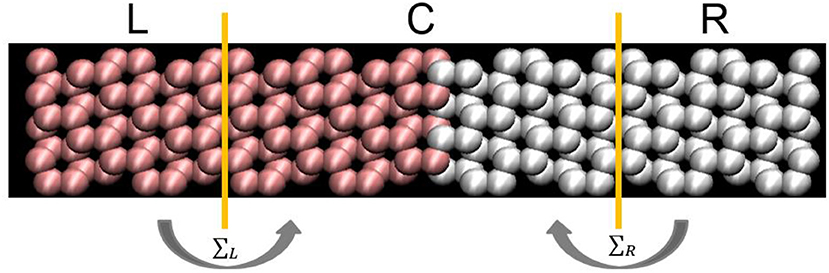
Figure 1. Silicon with perfect Σ3 grain boundary. The system is partitioned into three regions: left lead (L), center region (C), and right lead (R). Left and right leads are semi-infinite crystal lattices. All the three regions impose periodic boundary conditions in the transverse direction to represent the infinite lateral dimension. The grain boundary has 2 layers and each layer has 8 atoms. The unit cell of center region contains 96 atoms and the unit cell of each lead is composed of 48 atoms.
In Figure 2A, the transmission function of a perfect Σ3 grain boundary does not drop significantly compared to the pure silicon case. The overall thermal conductance of the perfect Σ3 grain boundary case decreases only 15% at room temperature as shown in Figure 2B, indicating that perfect grain boundary itself does not have significant impact on phonon transmission. This phenomenon is similar to the electron transport case where defect-free grain boundaries are almost transparent to electron transport in highly symmetric grain boundaries [8]. However, in real samples, the defect-free grain boundaries rarely exist [37].
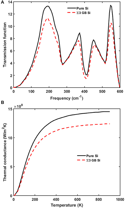
Figure 2. (A) Phonon transmission, and (B) thermal conductance for pure silicon (black solid line) and silicon with perfect Σ3 grain boundary (red dashed line).
Then we evaluate the influence of the disorders or defects at the grain boundary. The simple treatment for the disorders or defects used in this work is not exact or rigorous, but should provide a general idea. We calculate the dangling bonds case by randomly deleting the bonds at the grain boundary to mimic point defects or impurities. In Figure 3, the phonon transmission and thermal conductance keeps decreasing as the number of dangling bonds increases. The thermal conductance is reduced by 60% when half of the bonds at the grain boundary are deleted.
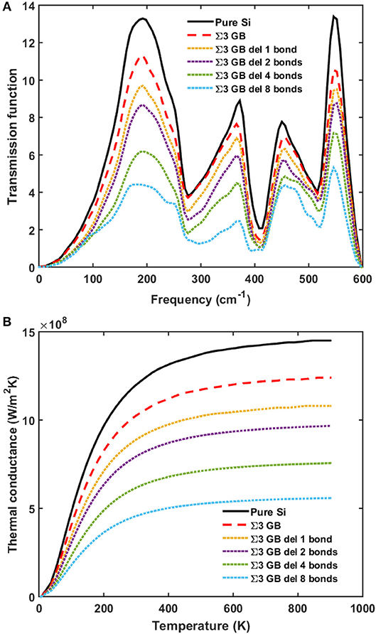
Figure 3. (A) Phonon transmission and (B) thermal conductance for pure silicon (black solid line), silicon with perfect Σ3 grain boundary (red dashed line), and silicon with defective Σ3 grain boundary with dangling bonds (dotted lines).
We then randomly delete atoms from the two layers at the grain boundary to mimic the vacancy case. More significant reduction in the phonon transmission and thermal conductance is observed as in Figures 4, 5. The total thermal conductance decreases by 80% when half of the atoms are missing. The reason for the larger reduction in the case of missing atoms compared with that in the case of dangling bonds is that missing atoms makes the grain boundaries more defective.
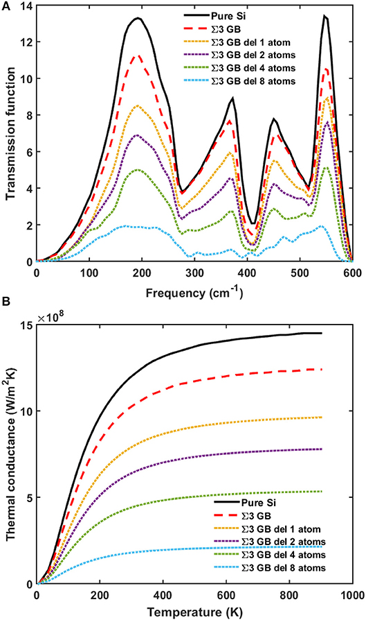
Figure 4. (A) Phonon transmission and (B) thermal conductance for pure silicon (black solid line), silicon with perfect Σ3 grain boundary (red dashed line), and silicon with defective Σ3 grain boundary with missing atoms (dotted lines).
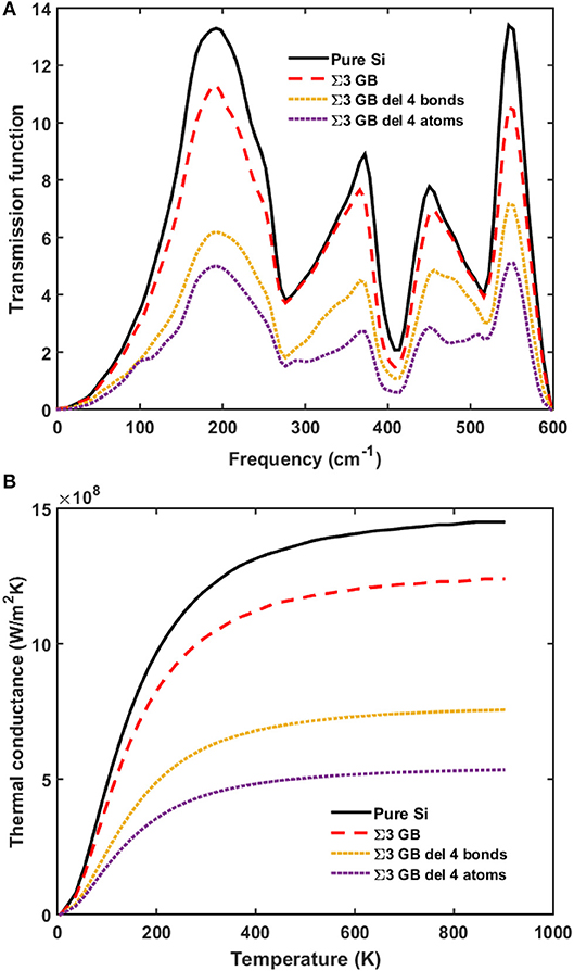
Figure 5. (A) Phonon transmission and (B) thermal conductance for pure silicon (black solid line), silicon with perfect Σ3 grain boundary (red dashed line), and silicon with defective Σ3 grain boundary with dangling bonds (yellow dotted line), and missing atoms (purple dotted line).
Conclusion
In summary, we apply atomistic Green's function method to investigate the phonon transmission across Σ3 grain boundaries of silicon and the overall thermal conductance. The results indicate that similar to electron transport, the perfect grain boundary does not significantly reduce thermal conductance, but defective grain boundaries can dramatically reduce the thermal conductance. This work may help understand the underlying thermal transport mechanism across grain boundaries.
Author Contributions
All authors listed have made a substantial, direct and intellectual contribution to the work, and approved it for publication.
Conflict of Interest Statement
The authors declare that the research was conducted in the absence of any commercial or financial relationships that could be construed as a potential conflict of interest.
Acknowledgments
This work is sponsored by the Department of the Navy, Office of Naval Research under ONR award number N00014-18-1-2724. This work used the Extreme Science and Engineering Discovery Environment (XSEDE), which is supported by National Science Foundation Grant ACI-1053575.
References
1. Wang Z, Alaniz JE, Jang W, Garay JE, Dames C. Thermal conductivity of nanocrystalline silicon: importance of grain size and frequency-dependent mean free paths. Nano Lett. (2011) 11:2206–13. doi: 10.1021/nl1045395
2. Romero MJ, Liu F, Kunz O, Wong J, Jiang CS, Al-Jassim M, et al. Imaging electron transport across grain boundaries in an integrated electron and atomic force microscopy platform: application to polycrystalline silicon solar cells. MRS Online Proc Libr Arch. (2009) 1153:A15-03. doi: 10.1557/PROC-1153-A15-03
3. Yamamoto T, Sato Y, Tanaka T, Hayashi K, Ikuhara Y, Sakuma T, et al. Electron transport behaviors across single grain boundaries in n-type BaTiO3, SrTiO3 and ZnO. J Mater Sci. (2005) 40:881–7. doi: 10.1007/s10853-005-6505-4
4. Zhang Y, Wang X, Zheng X, Chen G, Ma D, Xu F, et al. Effect of grain boundary scattering on electron mobility of N-polarity inN films. Appl Phys Express (2013) 6:21001. doi: 10.7567/APEX.6.021001
5. Wallace SK, McKenna KP. Grain boundary controlled electron mobility in polycrystalline titanium dioxide. Adv Mater Interfaces (2014) 1:1400078. doi: 10.1002/admi.201400078
6. Vancsó P, Márk GI, Lambin P, Mayer A, Kim YS, Hwang C, et al. Electronic transport through ordered and disordered graphene grain boundaries. Carbon (2013) 64:101–10. doi: 10.1016/j.carbon.2013.07.041
7. Majee AK, Foss CJ, Aksamija Z. Impact of mismatch angle on electronic transport across grain boundaries and interfaces in 2D materials. Sci Rep. (2017) 7:16597. doi: 10.1038/s41598-017-16744-0
8. Zhang H, Lee G, Gong C, Colombo L, Cho K. Grain boundary effect on electrical transport properties of graphene. J Phys Chem C (2014) 118:2338–43. doi: 10.1021/jp411464w
9. Cheng W, Ren SF. Size effect of thermal conductivity of Si nanocrystals. Solid State Commun. (2008) 147:274–7. doi: 10.1016/j.ssc.2008.06.001
10. Ju S, Liang X, Xu X. Out-of-plane thermal conductivity of polycrystalline silicon nanofilm by molecular dynamics simulation. J Appl Phys. (2011) 110:54318. doi: 10.1063/1.3633232
11. Amrit J. Grain boundary kapitza resistance and grain-arrangement induced anisotropy in the thermal conductivity of polycrystalline niobium at low temperatures. J Phys D Appl Phys. (2006) 39:4472. doi: 10.1088/0022-3727/39/20/026
12. Seager CH. Grain boundaries in polycrystalline silicon. Annu. Rev. Mater. Sci. (1985) 15:271–302.
13. Nan CW, Birringer R. Determining the Kapitza resistance and the thermal conductivity of polycrystals: a simple model. Phys Rev B (1998) 57:8264.
14. Dong H, Wen B, Melnik R. Relative importance of grain boundaries and size effects in thermal conductivity of nanocrystalline materials. Sci Rep. (2014) 4:7037. doi: 10.1038/srep07037
15. Maldovan M. Thermal energy transport model for macro-to-nanograin polycrystalline semiconductors. J Appl Phys. (2011) 110:114310. doi: 10.1063/1.3665211
16. Wang S,. Thermal Conductivity of Nanocrystalline Nickel. Master thesis. University of Toronto (2011). Available online at: https://tspace.library.utoronto.ca/bitstream/1807/31628/1/Wang_Shize_201111_MASc_Thesis.pdf
17. Yang HS, Bai GR, Thompson LJ, Eastman JA. Interfacial thermal resistance in nanocrystalline yttria-stabilized zirconia. Acta Mater. (2002) 50:2309–17. doi: 10.1016/S1359-6454(02)00057-5
18. Cahill DG, Ford WK, Goodson KE, Mahan GD, Majumdar A, Maris HJ, et al. Nanoscale thermal transport. J Appl Phys. (2003) 93:793–818. doi: 10.1063/1.1524305
19. Soyez G, Eastman JA, Thompson LJ, Bai GR, Baldo PM, McCormick AW, et al. Grain-size-dependent thermal conductivity of nanocrystalline yttria-stabilized zirconia films grown by metal-organic chemical vapor deposition. Appl Phys Lett. (2000) 77:1155–7. doi: 10.1063/1.1289803
20. Spiteri D, Anaya J, Kuball M. The effects of grain size and grain boundary characteristics on the thermal conductivity of nanocrystalline diamond. J Appl Phys. (2016) 119:85102. doi: 10.1063/1.4942522
21. Ashmawi WM, Zikry MA. Grain boundary effects and void porosity evolution. Mech Mater. (2003) 35:537–52. doi: 10.1007/978-94-017-0483-0_35
22. Goel N, Webb III EB, Rickman JM, Oztekin A, Neti S. Thermal transport across symmetric tilt grain boundaries in β-SiC: effect of dopants and temperature. AIP Adv. (2016) 6:75101. doi: 10.1063/1.4955431
23. Zebarjadi M, Esfarjani K, Dresselhaus MS, Ren ZF, Chen G. Perspectives on thermoelectrics: from fundamentals to device applications. Energy Environ Sci. (2012) 5:5147–62. doi: 10.1039/C1EE02497C
24. Tian Z, Lee S, Chen G. Heat transfer in thermoelectric materials and devices. J Heat Transf. (2013) 135:61605. doi: 10.1115/1.4023585
25. Millett PC, Wolf D, Desai T, Rokkam S, El-Azab A. Phase-field simulation of thermal conductivity in porous polycrystalline microstructures. J Appl Phys. (2008) 104:33512. doi: 10.1063/1.2964116
26. Li N, Ren J, Wang L, Zhang G, Hanggi P, Li B, et al. Colloquium: phononics: manipulating heat flow with electronic analogs and beyond. Rev Mod Phys. (2012) 84:1045. doi: 10.1103/RevModPhys.84.1045
27. Schelling PK, Phillpot SR, Keblinski P. Kapitza conductance and phonon scattering at grain boundaries by simulation. J Appl Phys. (2004) 95:6082–91. doi: 10.1063/1.1702100
28. Kimmer C, Aubry S, Skye A, Schelling PK. Scattering of phonons from a high-energy grain boundary in silicon: dependence on angle of incidence. Phys Rev B (2007) 75:144105. doi: 10.1103/PhysRevB.75.144105
29. Zheng Z, Chen X, Deng B, Chernatynskiy A, Yang S, Xiong L, et al. Phonon thermal transport through tilt grain boundaries in strontium titanate. J Appl Phys. (2014) 116:73706. doi: 10.1063/1.4893648
30. Mingo N, Yang L. Phonon transport in nanowires coated with an amorphous material: an atomistic Green's function approach. Phys Rev B (2003) 68:245406. doi: 10.1103/PhysRevB.68.245406
31. Zhang W, Fisher TS, Mingo N. The atomistic Green's function method: an efficient simulation approach for nanoscale phonon transport. Numer Heat Transf Part B Fundam. (2007) 51:333–49. doi: 10.1080/10407790601144755
32. Tian Z, Esfarjani K, Chen G. Enhancing phonon transmission across a Si/Ge interface by atomic roughness: first-principles study with the Green's function method. Phys Rev B (2012) 86:235304. doi: 10.1103/PhysRevB.86.235304
33. Tian Z, Esfarjani K, Chen G. Green's function studies of phonon transport across Si/Ge superlattices. Phys Rev B (2014) 89:235307. doi: 10.1103/PhysRevB.89.235307
34. Zhang W, Fisher TS, Mingo N. Simulation of interfacial phonon transport in Si–Ge Heterostructures using an atomistic green's function method. J Heat Transf. (2007) 129:483. doi: 10.1115/1.2709656
35. Ong ZY, Zhang G. Efficient approach for modeling phonon transmission probability in nanoscale interfacial thermal transport. Phys Rev B (2015) 91:174302. doi: 10.1103/PhysRevB.91.174302
36. Plimpton S. Fast parallel algorithms for short-range molecular dynamics. J Comput Phys. (1995) 117:1–19.
Keywords: atomistic Green's function, grain boundary, silicon, phonon transmission, thermal conductance
Citation: Li C and Tian Z (2019) Phonon Transmission Across Silicon Grain Boundaries by Atomistic Green's Function Method. Front. Phys. 7:3. doi: 10.3389/fphy.2019.00003
Received: 31 July 2018; Accepted: 08 January 2019;
Published: 29 January 2019.
Edited by:
Xiulin Ruan, Purdue University, United StatesReviewed by:
Adam Jan Gadomski, University of Science and Technology (UTP), PolandXiang Chen, Louisiana Tech University, United States
Copyright © 2019 Li and Tian. This is an open-access article distributed under the terms of the Creative Commons Attribution License (CC BY). The use, distribution or reproduction in other forums is permitted, provided the original author(s) and the copyright owner(s) are credited and that the original publication in this journal is cited, in accordance with accepted academic practice. No use, distribution or reproduction is permitted which does not comply with these terms.
*Correspondence: Zhiting Tian, emhpdGluZ0Bjb3JuZWxsLmVkdQ==