 Claudio Castellan
 Riccardo Franchi
 Stefano Biasi
 Martino Bernard
 Mher Ghulinyan
 Lorenzo Pavesi
- 1Nanoscience Laboratory, Department of Physics, University of Trento, Trento, Italy
- 2Centre for Materials and Microsystems, Fondazione Bruno Kessler, Trento, Italy
Silicon waveguides embedded in lateral p-n junctions show field-induced optical nonlinearities. By properly polarizing the junction, these can be used to achieve electro-optic modulation through the Direct Current Kerr effect. In addition, these enable second-order nonlinear processes such as the electric-field-induced second harmonic generation (EFISHG). In this work, we study in detail electro-optic effects in integrated silicon microresonators and demonstrate experimentally a field-induced resonance wavelength shift. This process is due to both the DC Kerr effect and the plasma-dispersion effect. By means of finite element method simulations, these effects are properly modeled and their contributions are accurately disentangled. The strength of the equivalent second-order nonlinear coefficient that would have provided the same electro-optic effect is about 16 pm/V. This result is comparable with that of materials possessing an intrinsic second order nonlinearity, and is one order of magnitude stronger than the most recent measurements of strain-induced Pockels effect in silicon.
1. Introduction
The study of nonlinear optical phenomena received raising interest in the last decades [1]. Most of the applications are based on second order nonlinear processes, which are enabled by lower optical power than the other higher order processes. Materials with large second order nonlinear susceptibilities, χ(2), such as Lithium Niobate (LN), Potassium Titanyl Phosphate (KTP) or Barium Borate (BBO) are widely used in Pockels cells and in frequency conversion [2–4]. Strong benefits could derive from the possibility to integrate these phenomena on a photonic chip. Integration will allow reducing the production cost and the power consumption, and to increase the nonlinear interaction strength [5]. Although the promising results have been recently reported in the integration of LN [6, 7], nowadays the technologies used to realize integrated devices with large-χ(2) materials are less advanced than the one based on silicon. In fact, the Complementary-Metal-Oxide-Semiconductor (CMOS) technology developed for microelectronics is well established, and this enabled the realization of high quality silicon-based devices [8]. However, due to the centrosymmetry of crystalline silicon, χ(2) processes are strongly inhibited [8]. Therefore, nonlinear silicon photonics makes use of the third order nonlinear susceptibilities χ(3) of silicon, with which different phenomena and a large variety of applications have been demonstrated [8]. However, the possibility to induce a non-zero χ(2) in silicon has been widely investigated [9], because it would enable interesting phenomena like Pockels effect, Second Harmonic Generation (SHG) or Spontaneous Parametric Down-Conversion (SPDC) [1]. Most of these attempts have been based on the deposition of a stressing silicon nitride cladding layer to strain the silicon waveguide and, consequently, to break the silicon centrosymmetry [10]. Even though positive results have been reported [10, 11], very recent works demonstrate that most of the reported measurements have been misinterpreted [12–15]. The χ(2) that can be induced in silicon by the strain is very low [16, 17]. On the other hand, a recent work has demonstrated an alternative way to enable effective χ(2) processes in silicon by making use of silicon rib waveguides with lateral doping forming a p-i-n junction [18]. In this way, a DC (direct current) electric field is induced inside the waveguide. This enables the so called Electric Field Induced SHG (EFISHG) in silicon, a process where the silicon χ(3) is mixed with the DC field to yield an effective χ(2). Making use of Mach-Zehnder interferometers, the authors of Timurdogan et al. [18] also demonstrated the DC Kerr effect, a χ(3) nonlinear process which can be used for electro-optic modulation.
In this work, we study in detail the field-induced nonlinear processes in integrated silicon microresonators with lateral junctions. Doing so, we study both the plasma-dispersion effect and the DC Kerr effect, which are processes that cause a variation of the effective refractive index of the resonator mode. We experimentally demonstrate the field-induced refractive index variation and, by properly modeling the system, we reproduce the experimental data. Then, we quantify the electro-optic coefficient for this system, comparing it with the most advanced studies in strained silicon, as well as with the other materials most commonly used for electro-optic modulation.
The work is organized as follows. In section 2, the geometry and the fabrication technique of the resonators analyzed in this work are described. In section 3, the main changes in the real part of refractive index induced by the applied electric field are introduced. Then, in section 4, the effect of the applied field on the imaginary component of the refractive index is studied in detail. First, a model capable to extract the absorption coefficient from the resonator transmission spectrum is shown. Then, the system is modeled using Finite Element Method (FEM) simulations, providing a proper description of the phenomena. In section 5, the effect of the applied field on the material refractive index is quantified and compared with experimental data. Finally, in section 6, the main conclusions and perspectives of this work are reported.
2. Microring Resonator Geometry
The top-view sketch of the microring resonator is shown in Figure 1A. It consists of a 150 μm radius microring in the all-pass configuration, realized by a silicon rib waveguide whose cross-section is sketched in Figure 1B. The waveguides are defined by a 365 nm UV lithography on a 6' Silicon-On-Insulator (SOI) wafer and realized by reactive ion etching. The slab height is 300 nm, while the waveguide's full height is 490 nm and its width is 550 nm. These values were chosen to obtain single mode operation at the wavelength of 1550 nm. The bus and the resonator waveguides have the same geometry, and are point-coupled with a minimum separation of 600 nm. Lateral doped regions are realized at a distance d from the waveguide borders. Different values of d are proposed in the design, respectively 200, 500, and 800 nm. The carrier concentration is 1 × 1018 cm−3 in both the n-type doped and in the p-type doped regions, while the waveguide has a residual 1 × 1015 cm−3 p-type doping as the original SOI device layer. A top oxide cladding is deposited through Plasma-Enhanced Chemical Vapor Deposition (PECVD) over the waveguides. Vias are created through the oxide to polarize the junctions via aluminum pads.
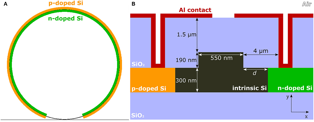
Figure 1. Top-view (A) and cross-section (B) of the resonators described in this work.
3. Field-Induced Optical Changes
In the microring resonator, both the material refractive index and its absorption are affected by the junction.
Absorption (or power losses) are enhanced due to defects introduced during the implantation of the dopants and/or to the presence of free-carriers. In fact, variations ΔNe and ΔNh of the electron and of the hole concentration induce a variation of the absorption coefficient Δα given by [19]:
The coefficients a, b, c, and d characterize each semiconductor, and are wavelength dependent. For silicon at the wavelength of 1550 nm, a ≈ 8.88 × 10⁻²¹ cm2, b ≈ 1.167, c ≈ 5.84 × 10⁻²⁰ cm2 and d ≈ 1.109 [19]. Variations of the material absorption modify the resonator's quality factor, and so they can be measured by analyzing the spectral features of the resonator. In the following, a reverse bias of the junction is considered. This reduces the charge concentration inside the waveguide and therefore also the free carrier losses.
The lateral p-n junctions affect also the material refractive index due to both the plasma-dispersion effect and the DC Kerr effect [18]. Plasma-dispersion is a linear optical effect caused by the variation of the free-carrier concentration. The material refractive index is modified by a quantity Δnpd given by [19]:
where for silicon at the wavelength of 1550 nm p ≈ 5.4 × 10⁻²² cm3, q ≈ 1.011, r ≈ 1.53 × 10⁻¹⁸ cm3 and s ≈ 0.838 [19]. DC Kerr effect is a third order nonlinear effect [1] that introduces a refractive index perturbation Δnk given by [20]:
Here n0 is the unperturbed refractive index and χ(3) is the third order nonlinear susceptibility, which for silicon at the wavelength of 1550 nm is 2.45 × 10⁻¹⁹ m2/V2 [21]. EDC is the applied DC field. Both the DC Kerr effect and the plasma-dispersion cause a variation of the material refractive index Δn = Δnpd + Δnk. This results in a variation Δneff of the resonator mode effective index, which in turn determines a shift Δλ of the microring resonator resonance wavelength given by [14, 22]:
being λ the resonance wavelength, ng the group index of the propagating mode and η the fraction of the resonator perimeter that undergoes the effective index variation (in this work η ~ 0.9, since the p-n junction is not present in the coupling region).
4. Field-Induced Absorption
4.1. Modeling the System via Transfer Matrix Methods
To extract losses from the resonator transmission spectra, a model to fit them is introduced. This model describes the system sketched in Figure 2A, consisting of a resonator in the all-pass configuration. We define the input and output electric field at the facet A (B) as and ( and ). The model considers that light is coupled into the system via butt coupling [23]. Due to the strong refractive index difference between the silicon waveguide and air, the coupling facets have a strong reflectance, forming a Fabry-Perot cavity whose transmission spectrum is superimposed to the resonator's one. The behavior of the whole system is described by the transfer matrix method:
M is a 2 × 2 transfer matrix defined as the product M = MF,BML,BMrML,AMF,A. In particular, MF,A and MF,B are the transfer matrices of the input and of the output facets, ML,A and ML,B are the transfer matrices describing the propagation in the bus waveguide between the coupling facets and the resonator, while Mr is the transfer matrix of the microring resonator.
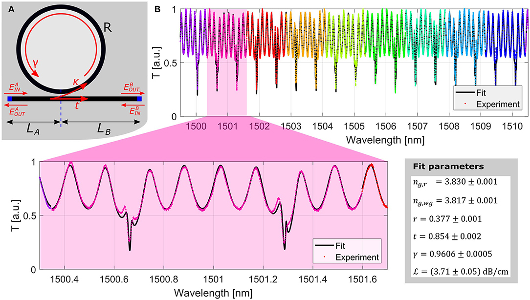
Figure 2. (A) Sketch of the device described in this work, showing the main parameters of the model. (B) Experimental spectrum of the resonator (dots) and corresponding fit (solid black lines). On the bottom, part of the fitted spectrum is enlarged. In the inset, the fit parameters are reported.
The transfer matrices describing the input and the output facets can be written as [24]:
being τA and τB the transmission coefficients of the input/output facets, while rA and rB are the corresponding reflection coefficients. These quantities are related by and . The matrices MF,A and MF,B have opposite sign on the anti-diagonal terms because of the opposite interfaces.
The transfer matrices describing the propagation in the bus waveguides are [24]:
being ϕA and ϕB the phases acquired between the input/output facets and the resonator. In general ϕj = (βj + iαj)Lj, being βj = 2πneff,j/λ the propagation constant, αj the absorption coefficient and Lj the waveguide length.
The transfer matrix of the resonator is given by [25]:
Here, t is the transmission coefficient of the bus waveguide-resonator coupler (related to the coupling coefficient κ by t2 = 1 − κ2) and γ is the roundtrip loss coefficient (it relates the power coupled into the resonator Pi with the power after one complete roundtrip Po by ). The coefficient ϕ is the phase acquired in a complete roundtrip, and is given by ϕ = βL, being L the resonator length and β = 2πneff/λ the propagation constant in the resonator waveguide. In Equation (8) the backreflection fields connected to the coupling region and/or to the surface wall roughness are neglected (i.e., the off-diagonal elements are equal to zero). The surface roughness is considered as a simple radiative loss within the γ coefficient.
By multiplying the matrices, one can derive the system transfer function T as:
This function can be used to fit the experimental transmission spectrum. Neglecting the ring resonator (i.e., t = 1) Equation (9) reduces to the response of a Fabry-Perot cavity: . Similarly, neglecting the Fabry-Perot induced by the facets (i.e., τA = τB = 1, rA = rB = 0, ϕA = ϕB = 0) one obtains the transmission amplitude of a single mode resonator:. In this case the transfer function is a set of symmetric Lorentzians and, depending on t and γ, the different coupling regimes of the microresonator can be identified: under-coupling (t > γ), critical-coupling (t = γ) and over-coupling (t < γ).
To simplify this model propagation losses are neglected in the bus waveguide (i.e., αj = 0), as the bus waveguide is just 2 mm long and so the dominant loss term is the reflectance of the facets. Moreover, being the input/output waveguide cross-section identical, we introduced r = rA = rB. Last, since the effective indices of the bus and the resonator waveguide modes are wavelength dependent, one can use the definition of the group index to write the propagation constants as [22]:
Therefore, the propagation constants have a wavelength-dependent term (related to the group index ng) and a constant term. Since β(λ) enters in Equation (9) in periodic functions, the fit can be used to uniquely determine the wavelength-dependent terms (so ng), but not the constant terms. So, using this simplified model, the fitting parameters are the bus waveguide and the resonator group indices (ng,wg and ng,r), the input/output waveguide reflectance r, the coupler transmission coefficient t and the roundtrip loss γ.
Figure 2B shows the experimental transmission spectrum of a microresonator without the p-n junction, divided by colors in groups of two resonances. Each group is fitted according to Equation (9), showing the fit result in black. The panel reports the fit parameters. The fit results show that t < γ, and therefore the resonator is in the over-coupling regime. The quality factor of all the resonators analyzed in this work, defined as the ratio between each resonant wavelength and its full-width at half-maximum, is in the order of 104. Figure 2B reports also the propagation loss coefficient , related to the loss coefficient γ and to the resonator length L by:
4.2. The Effect of Doping on the Microresonator Losses
Figure 3A shows the transmission coefficient t as a function of the distance d between the waveguide border and the doped regions extracted from the data with the method described in the previous section. Each point is the average of 4 measurements taken on nominally identical resonators. The measurement labeled by “R” refers to a reference resonator where no doping was present at the waveguide borders. As expected, t does not depend on the presence of the junctions, and so the values measured on resonators with different d are compatible.
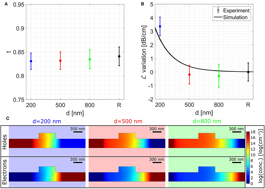
Figure 3. (A) Transmission coefficient t as a function of the distance d between the waveguide border and the doped region. The label by “R” refers to a reference resonator without doped regions. (B) Variation of the loss coefficient with respect to the reference case. The experimental data are compared with simulations. (C) Electron and hole distribution inside the waveguide for different d.
This is not the case if one considers the roundtrip loss coefficient γ or, equivalently, the loss coefficient . To this purpose, Figure 3B shows as a function of d, normalized over the value assumed by the reference resonator. The figure shows that decreases as d increases. This is attributed to the fact that, when d is smaller, the optical mode overlaps with the doped region, and so the losses are larger.
To make a more quantitative assesment of the effect of d on the losses, the system is modeled using the Semiconductor Module of the COMSOL Multiphysics® software [26]. Some results of this simulation are shown in Figure 3C, where the electron and the hole distribution in the waveguide for different d are reported. Using these maps and Equation (1), the corresponding carrier-induced variation of the absorption coefficient Δα is estimated. By inserting Δα in the Mode Analysis tool of the Wave Optics Module of the COMSOL Multiphysics® software [26], the corresponding variation of the loss coefficient is evaluated. This simulated value is reported as a function of d in Figure 3B, reproducing the behavior of the experimental data.
4.3. Modeling the Junction Breakdown
Figure 4A shows the measured I-V curve of the three types of devices analyzed in this work, referred to d = 200, 500, and 800 nm. They show the typical curve of a diode, with the expected behavior in both forward and reverse bias. The breakdown voltage Vb is different for the three structures. As it is also shown in Table 1, larger Vb values are measured for larger values of d.
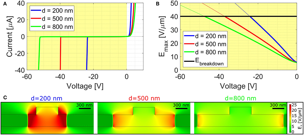
Figure 4. (A) Measured I-V curves of three devices analyzed in this work, referred to d = 200, 500, and 800 nm. (B) Simulated maximum field inside the waveguide as a function of the bias voltage and for the three different d, compared to the breakdown field of silicon (black). (C) Electric field distribution inside the waveguide for different values of d and for a reverse bias of 20 V.
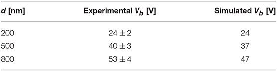
Table 1. Experimental and simulated values of the breakdown voltage Vb for the different values of d.
Using the same simulation tool described before, the electric field distribution inside the waveguide has been obtained for different values of the applied bias. Figure 4C shows this distribution for the three values of d analyzed in this work and for a reverse bias of 20 V. The figure shows that, as d increases, the electric field inside the waveguide decreases. To relate this to the breakdown, Figure 4B reports the maximum field inside the waveguide Emax as a function of the bias voltage and for the three different d. Breakdown is reached when Emax approaches the breakdown field of silicon, which is about 40 V/μm [27] and is reported by the black line in the figure. So, by comparing the breakdown field value and the results of the simulation, one can guess the expected voltage which provides breakdown. The values for the different d are reported in Table 1, showing good agreement with the experiment.
4.4. The Effect of Bias on Microresonator Losses
Figure 5A shows the variation of the loss coefficient as a function of the applied bias voltage. This factor is evaluated from the fit of the resonances, and is normalized over the value measured at zero bias. The loss variation is nonzero only for d = 200 nm. This loss change can be attributed to a variation of the carrier concentration inside the waveguide, which causes a reduction of the optical absorption.
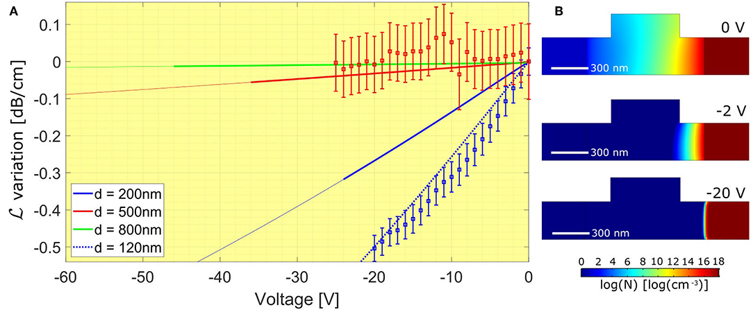
Figure 5. (A) Experimental (points) and simulated (solid lines) variation of the loss coefficient as a function of the applied bias voltage for d = 200 nm, d = 500 nm and d = 800 nm. In the case d = 800 nm the experimental values are not shown for clarity, because they are very similar to those for d = 500 nm. The dotted line refers to d = 120 nm. (B) Simulated electron concentration inside the waveguide for d = 200 nm and different values of the applied bias voltage.
To model this, Figure 5B shows the simulated electron concentration inside the waveguide in the configuration d = 200 nm for three different reverse bias voltages (0 V, 2 V and 20 V). The simulation shows the bias dependence of the junction depletion. Clearly, the change felt by the optical mode is larger if d is small, and this can explain why is more affected by the bias for small d.
The carrier concentration map shown in Figure 5B can be used together with Equation (1) to estimate the loss coefficient variation Δα, and so to estimate the corresponding variation of . The results of the simulations are reported in Figure 5A as a function of the applied bias. While for d = 500 nm and d = 800 nm the simulation predicts a small variation which is in agreement with the experiment, for d = 200 nm the loss variation predicted by simulations is smaller than the experiment. This is due to a difference between the nominal d and its actual value, which is smaller due to the ion implantation process. Specifically, as we discuss later, a mask shadow effect caused by the angled implantation justifies a wider-than-expected doped region. To this purpose, a simulation with a smaller d has been performed. The dashed line of Figure 5A refers d = 120 nm, and provides a good agreement with the experiment.
5. Field-Induced Refractive Index Variation
In section 3 we introduced that the material refractive index is expected to change due to both plasma-dispersion and DC Kerr effect when applying a bias. This refractive index change causes a shift of the resonance wavelength, as expressed by Equation (4). To quantify this variation, we used the same simulation tool described previously to model both the electron and the hole densities as well as the electric field distribution inside the waveguide. These quantities are then used to quantify the refractive index variations due to plasma-dispersion and Kerr effect according to Equations (2) and (3). Once that these are known, a mode analysis simulation can provide the effective refractive index variation Δneff. To this purpose Figure 6A shows the applied voltage dependence of the different contributions to Δneff. In the same plot on the right hand axis, it is reported the resonant wavelength shift Δλ calculated from Equation (4). Both the plasma dispersion and the DC Kerr effect contributions cause a red-shift of the resonant wavelength. This simulation refers to the configuration d = 200 nm.
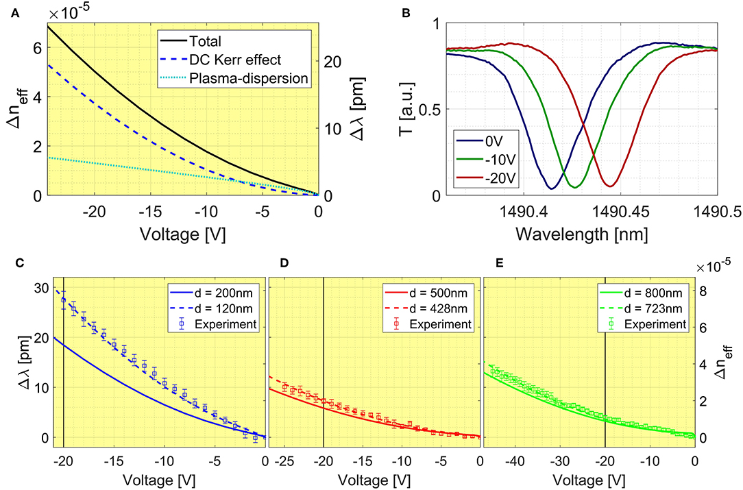
Figure 6. (A) Simulated effective index variation and corresponding resonance wavelength shift for d = 200 nm considering plasma-dispersion, DC Kerr effect and both the effects. (B) Transmission spectrum of the resonator with d = 200 nm and for different values of the reverse bias. (C–E) Comparison between the experimental and the simulated resonance wavelength shift for d = 200 nm, d = 500 nm, and d = 800 nm.
Figure 6B reports the transmission spectra of the microring resonator for the configuration d = 200 nm and for three different values of the applied reverse bias. As expected, we observe a resonance wavelength shift to the red. Moreover, the shift is not linear with the applied bias, as predicted by the simulation. It is worth noting that, in our case, the presence of the p-n junction induces an increase of the extinction rate. In fact, the junction boosts the linear losses which means in our model a decrease of the coefficient γ. Therefore, the resonator coupled to a bus waveguide moves from an over-coupling regime toward an under-coupling one. The voltage dependence of the resonance shift is reported in Figures 6C–E for the values of d analyzed in this work. The experimental results (squares) are compared with simulated results (solid lines). It is observed that Δλ decreases with d for a given voltage. However, the simulations predict resonance wavelength variations smaller than the experimental ones. This is due to the difference between the nominal and actual value of d. For this purpose, new simulations have been performed aimed at finding the best d value to reproduce the experimental data. These simulations are shown as dashed lines. We find that the actual d is smaller than the nominal one by almost 75 nm for the three devices. This value is the same as the one reported in section 4.4 on the measured variation of the absorption coefficient.
To understand this difference, one must consider the details of the sample fabrication. Specifically, the ion implantation was performed by using the typical angle θ = 7° with respect to the normal to the sample surface, which allows a precise definition of the implantation depth. So, the actual d is reduced by Δd = −htanθ, where h is the height of the photoresist used to define the structures. Since in our case h = 650 nm, Δd is about −80 nm, in agreement with the results found from the experiment.
Interestingly, we observe that the plasma dispersion and the DC Kerr effect have similar relevance at low bias, while the DC Kerr effect dominates at high bias. This is important for electro-optic applications since the DC Kerr effect provides a faster response than the slow modulation of the plasma dispersion. Indeed plasma dispersion response time is limited by the carrier mobility.
The most common material platforms used to induce electro-optic effects are based on Pockels effect, a χ(2) process providing a linear electro-optic variation of the material refractive index with the applied voltage. For this reason, it is interesting to estimate the effective second order nonlinearity that would have given the same electro-optic refractive index variation as the here measured DC Kerr effect. For the Pockels effect, the index variation Δneff caused by an applied electric field E is related to χ(2) by [14]:
Figure 6A shows that, in the case d = 200 nm, an effective index variation of about 5 × 10⁻⁵ is obtained due to DC Kerr effect at a reverse bias of 23 V. In this situation, FEM simulations show that the average electric field inside the waveguide is about 20 V/μm. By using Equation (12) we estimate an equivalent of about 16 pm/V. This value is of the same order of magnitude of that of LN, whose χ(2) is 39 pm/V [28], and one order of magnitude stronger than the most recent measurement of Pockels effect in strained-silicon, which is about 1.8 pm/V [16].
6. Conclusions
In this work we have confirmed that rib silicon waveguides embedded in lateral p-n junction can be used to induce electro-optic effects [18]. Making use of microring resonators, we measured the effect that the doping and the applied bias have on the refractive index and loss coefficient of the waveguides. We used FEM simulations to reproduce the experimental data and to evidence the contributions of both plasma-dispersion and DC Kerr effect. We also quantified the strength of the equivalent that would have provided the same electro-optic effect as the observed DC Kerr effects, finding a value of about 16 pm/V. This large value is comparable to that of LN and one order of magnitude stronger than the most recent measurement of Pockels effect in strained-silicon. An efficient engineering of the waveguide cross-section could provide even larger electro-optic coefficients, which could benefit from the use of smaller and thinner waveguides where the electric field intensity is larger.
Data Availability
The datasets generated for this study are available on request to the corresponding author.
Author Contributions
CC designed the structures and conceived the experiment. CC and RF performed the experiments and the FEM simulations. CC, RF, SB, and MB developed the theoretical model to fit the spectra. MB and MG realized the samples and provided support in the design procedure. LP supervised the entire work. CC wrote the manuscript, which was revised by all the co-authors.
Funding
This work was supported by the Siquro project (Bando grandi progetti, Provincia Autonoma di Trento, 2012) and by the NEMO project (PRIN 2015KEZNYM supported by MIUR).
Conflict of Interest Statement
The authors declare that the research was conducted in the absence of any commercial or financial relationships that could be construed as a potential conflict of interest.
Acknowledgments
We acknowledge past and current members of the Nanoscience Laboratory for the beneficial interaction and support, and the fabrication facility support by the MicroNano Fabrication Laboratory of FBK. This work was also part of the Ph.D. thesis [20].
References
2. Arizmendi L. Photonic applications of lithium niobate crystals. Phys Status Solidi. (2004) 201:253–83. doi: 10.1002/pssa.200303911
3. Shur VY, Pelegova EV, Akhmatkhanov AR, Baturin IS. Periodically poled crystals of KTP family: a review. Ferroelectrics. (2016) 496:49–69. doi: 10.1080/00150193.2016.1157437
4. Fedorov PP, Kokh AE, Kononova NG. Barium borate β-BaB2O4 as a material for nonlinear optics. Russ Chem Rev. (2002) 71:651. doi: 10.1070/RC2002v071n08ABEH000716
5. Foster MA, Turner AC, Lipson M, Gaeta AL. Nonlinear optics in photonic nanowires. Opt Exp. (2008) 16:1300–20. doi: 10.1364/OE.16.001300
6. Wang C, Zhang M, Chen X, Bertrand M, Shams-Ansari A, Chandrasekhar S, et al. Integrated lithium niobate electro-optic modulators operating at CMOS-compatible voltages. Nature. (2018) 562:101. doi: 10.1038/s41586-018-0551-y
7. He M, Xu M, Ren Y, Jian J, Ruan Z, Xu Y, et al. High-performance hybrid silicon and lithium niobate Mach-Zehnder modulators for 100 Gbit/s and beyond. Nat Photon. (2019) 13:359. doi: 10.1038/s41566-019-0378-6
8. Borghi M, Castellan C, Signorini S, Trenti A, Pavesi L. Nonlinear silicon photonics. J Opt. (2017) 19:093002. doi: 10.1088/2040-8986/aa7a6d
9. Cazzanelli M, Schilling J. Second order optical nonlinearity in silicon by symmetry breaking. Appl Phys Rev. (2016) 3:011104. doi: 10.1063/1.4941558
10. Jacobsen RS, Andersen KN, Borel PI, Fage-Pedersen J, Frandsen LH, Hansen O, et al. Strained silicon as a new electro-optic material. Nature. (2006) 441:199–202. doi: 10.1038/nature04706
11. Cazzanelli M, Bianco F, Borga E, Pucker G, Ghulinyan M, Degoli E, et al. Second-harmonic generation in silicon waveguides strained by silicon nitride. Nat Mater. (2012) 11:148–54. doi: 10.1038/nmat3200
12. Azadeh SS, Merget F, Nezhad MP, Witzens J. On the measurement of the Pockels effect in strained silicon. Opt Lett. (2015) 40:1877–80. doi: 10.1364/OL.40.001877
13. Borghi M, Mancinelli M, Merget F, Witzens J, Bernard M, Ghulinyan M, et al. High-frequency electro-optic measurement of strained silicon racetrack resonators. Opt Lett. (2015) 40:5287–90. doi: 10.1364/OL.40.005287
14. Borghi M, Mancinelli M, Bernard M, Ghulinyan M, Pucker G, Pavesi L. Homodyne detection of free carrier induced electro-optic modulation in strained silicon resonators. J Lightwave Technol. (2016) 34:5657–68. doi: 10.1109/JLT.2016.2628183
15. Olivares I, Angelova T, Sanchis P. On the influence of interface charging dynamics and stressing conditions in strained silicon devices. Sci Rep. (2017) 7:7241. doi: 10.1038/s41598-017-05067-9
16. Berciano M, Marcaud G, Damas P, Roux XL, Crozat P, Ramos CA, et al. Fast linear electro-optic effect in a centrosymmetric semiconductor. Commun Phys. (2018) 1:64. doi: 10.1038/s42005-018-0064-x
17. Castellan C, Trenti A, Vecchi C, Marchesini A, Mancinelli M, Ghulinyan M, et al. On the origin of second harmonic generation in silicon waveguides with silicon nitride cladding. Sci Rep. (2019) 9:1088. doi: 10.1038/s41598-018-37660-x
18. Timurdogan E, Poulton CV, Byrd MJ, Watts MR. Electric field-induced second-order nonlinear optical effects in silicon waveguides. Nat Photon. (2017) 11:200–6. doi: 10.1038/nphoton.2017.14
19. Nedeljkovic M, Soref R, Mashanovich GZ. Free-carrier electrorefraction and electroabsorption modulation predictions for silicon over the 1–14-μm infrared wavelength range. IEEE Photon J. (2011) 3:1171–80. doi: 10.1109/JPHOT.2011.2171930
20. Castellan C. Second order nonlinearities in silicon photonics. (Ph.D thesis). University of Trento (2019). Available online at: http://eprints-phd.biblio.unitn.it/3543/
21. Hon NK, Soref R, Jalali B. The third-order nonlinear optical coefficients of Si, Ge, and Si1−xGex in the midwave and longwave infrared. J Appl Phys. (2011) 110:011301. doi: 10.1063/1.3592270
22. Bogaerts W, Heyn PD, Vaerenbergh TV, Vos KD, Selvaraja SK, Claes T, et al. Silicon microring resonators. Laser Photon Rev. (2012) 6:47–73. doi: 10.1002/lpor.201100017
23. Reed GT, Knights AP. Silicon Photonics: An Introduction. Chichester, UK: Wiley (2004). Available online at: https://books.google.it/books?id=bi4xpCk-ImIC
25. Yariv A. Critical coupling and its control in optical waveguide-ring resonator systems. IEEE Photon Technol Lett. (2002) 14:483–5. doi: 10.1109/68.992585
26. COMSOL Multiphysics. COMSOL Multiphysics® v. 5.3a. Stockholm: COMSOL AB. (2018). Available online at: https://www.comsol.com
27. Soref R, Bennett B. Electrooptical effects in silicon. IEEE J Quant Electr. (1987) 23:123–9. doi: 10.1109/JQE.1987.1073206
Keywords: nonlinear optics, silicon photonics, Kerr effect, field-induced nonlineatiries, plasma-dispersion effect, p-n junctions, microring resonator
Citation: Castellan C, Franchi R, Biasi S, Bernard M, Ghulinyan M and Pavesi L (2019) Field-Induced Nonlinearities in Silicon Waveguides Embedded in Lateral p-n Junctions. Front. Phys. 7:104. doi: 10.3389/fphy.2019.00104
Received: 20 May 2019; Accepted: 05 July 2019;
Published: 23 July 2019.
Edited by:
Shinichi Saito, University of Southampton, United KingdomReviewed by:
Isao Tomita, National Institute of Technology, Gifu College, JapanJunichi Fujikata, Photonics Electronics Technology Research Association, Japan
Copyright © 2019 Castellan, Franchi, Biasi, Bernard, Ghulinyan and Pavesi. This is an open-access article distributed under the terms of the Creative Commons Attribution License (CC BY). The use, distribution or reproduction in other forums is permitted, provided the original author(s) and the copyright owner(s) are credited and that the original publication in this journal is cited, in accordance with accepted academic practice. No use, distribution or reproduction is permitted which does not comply with these terms.
*Correspondence: Claudio Castellan, Y2xhdWRpby5jYXN0ZWxsYW5AdW5pdG4uaXQ=