 Stefano Signorini
 Matteo Finazzer
 Martino Bernard
 Mher Ghulinyan
 Georg Pucker2
 Lorenzo Pavesi
- 1Nanoscience Laboratory, Department of Physics, University of Trento, Trento, Italy
- 2Bruno Kessler Foundation, Centre for Materials and Microsystems, Trento, Italy
We design, fabricate and test an integrated silicon photonics chip for inter-modal four wave mixing, whose phase-matching relays on the modal dispersions of different waveguide modes. This phase-matching technique allows for tunable and broadband wavelength conversion and generation. We demonstrate that idler and signal photons can be generated with 800 nm spectral distance in between. We measure several inter-modal combinations, with up to the third order mode involvement. We demonstrate a maximum conversion efficiency of –12.4 dB from 1,468.5 to 1,641.1 nm with a bandwidth of 11 nm. We also prove the high and broadband tunability of the generated signal by scanning the pump wavelength when the signal wavelength is fixed. All these features make the inter-modal four wave mixing a viable solution for all optical processing in the near as well as in the mid infrared and for quantum applications.
1. Introduction
Nowadays, silicon photonics is a viable technique to satisfy the demand of high speed communication and high frequency computing. The development of technologies like wavelength division multiplexing (WDM) and mode division multiplexing (MDM) on an integrated platform is pushing the data rate to higher speeds [1, 2]. Here, MDM is useful to further increase the communication bandwidth. In order to deal with the waveguide modes non-linear optics is used, which enables all optical operations like wavelength conversion and switching. In this framework, an interesting approach is the use of inter-modal four wave mixing (FWM) [3]. FWM is a non-linear third order optical process in which two input pump photons are annihilated with the instantaneous generation of two photons at wavelengths different from the pump photon ones. When the FWM is inter-modal, the involved waves are propagating on different waveguide modes. Via inter-modal FWM new operations, such as mode selective wavelength conversion [4, 5], are possible. The increased flexibility provided by the waveguide modes allows broadband and tunable wavelength conversion. This has been already demonstrated in a multimode silicon waveguide [6], with the generated idler photons spanning from 1,200 to 1,500 nm. The broadband operation is one of the most interesting and exploited properties of inter-modal FWM in the integrated platform [7–9]. This property is of great interest not only for signal processing but also for on-chip sensing [10] and for integrated quantum photonics [11]. In fact, common to these applications is the need of a tunable source of photons. On-chip sensing would benefit of an integrated source of photons able to probe the gasses in their fingerprint spectral region [12], which extends in the mid infrared (MIR). Therefore, due to its broadband generation, inter-modal FWM can be used as an on-chip source of MIR photons [13]. Moreover, wavelength conversion by FWM can be used to spectral translate MIR photons in the near infrared (NIR), where efficient detectors exist. Indeed, direct detection of MIR photons is problematic and up-conversion is at the moment a reliable solution [14]. MIR is also of great interest for quantum photonics. Here, FWM can be used as a source of entangled or single photon states [15]. In particular, the generation of quantum states of light in the MIR is appealing for quantum sensing [16] or for quantum communication [17]. MIR is the region where many gasses have a characteristic molecular absorption and where several transparent atmospheric windows allow for low loss free space data exchange. Finally, the high control of the FWM process allows generating correlated pairs far from Raman or pump noises.
With respect to the first demonstration of inter-modal FWM on the silicon-on-insulator (SOI) platform, where simple multimode waveguides have been used [6], in this work we report the results obtained with an optimized design where the different modes are handled directly on the chip. In fact, inter-modal FWM requires efficient mode couplers to selectively route/couple different modes along the chip. Here, we use asymmetric directional couplers. This design has been initially proposed in Temporao et al. [18]. A similar design has been later used for on-chip entangled photons generation [19]. In the present work we show that this design is suitable for different inter-modal combinations, involving up to the third order mode. We also compare the efficiency and broadband operation of inter-modal FWM with the intra-modal FWM, where all the involved waves propagate on the very same mode. We show that the inter-modal FWM allows covering the spectral region from 1,200 to 1,500 nm with a high control and a maximum conversion efficiency of –12.4 dB.
The paper is organized as follow. In section 2 the inter-modal FWM is described, highlighting its main features. Particular attention is devoted to the dependence of the efficiency on the waveguide width and modal combination. In section 3 the chip design and the experimental set-up used are discussed. Two designs are proposed, for two different types of inter-modal combinations. In section 4 the results of the experimental measurements are reported. Section 5 concludes the paper.
2. Inter-modal Four Wave Mixing
FWM is a non-linear third order optical process involving four waves in a χ(3) medium. In FWM two pump waves combine together in order to produce two new harmonics, the signal and the idler waves. The basic requirement for this process to take place is energy conservation, while for an efficient generation a phase-matching condition has to be satisfied [20]. The phase-matching condition, directly related to the momentum conservation, can be written as:
where the indices p1, p2, s, i refer to the first pump, second pump, signal and idler photons, respectively. In order to quantify the quality of the phase-matching, the phase mismatch Δk is introduced as:
where ΔkL = ks+ki−kp1−kp2 is the linear phase mismatch and quantifies the phase contribution to Δk due to the self phase modulation (SPM) and cross phase modulation (XPM) of the pump waves [5]. and are the non-linear coefficients of the SPM, and are the non-linear coefficients of the XPM and Pp1, Pp2 are the powers of the two pump waves [21].
ΔkL in a multimode waveguide can be written as Borghi et al. [22]:
where j, q, l, m refer to the waveguide modes of the pumps, signal and idler, respectively. In the following, we use the convention that the modal combination involved in the FWM process is indicated as jqlm, i.e., one pump photon on the j-th order mode, the other pump photon on the q-th order mode, the signal photon on the l-th order mode and the idler photon on the m-th order mode. If j, q, l, m are all equal, the process is called intra-modal FWM, while if they are different the process is called inter-modal. Intra-modal FWM is the most investigated process in silicon, and it has been used for broad band generation and wavelength conversion [23]. However, its phase-matching is limited to the vicinity of the pump wavelength. This hinders the FWM to achieve very large detunings between idler and signal. The most investigated solution is the engineering of the group velocity dispersion (GVD), used for broadband FWM and large spectral conversion [23, 24]. The best results obtained in a SOI device with a C-band pump via GVD engineering are a 3-dB bandwidth of 150 and 195 nm maximum spectral translation with –12 dB efficiency [23]. However, the GVD engineering approach is limited in tunability and it is highly fabrication dependent.
With inter-modal FWM, the pumps, signal and idler propagate on different modes. As an example, in Figure 1 (right) the mode profiles involved in the 1221 TE (transverse electric polarization) combination in a rib waveguide are shown. Each waveguide mode has a different effective index and is affected differently by the waveguide engineering [6]. According to Equation (3), by properly choosing the waveguide geometry and the involved modes, Δk can be made equal to zero (i.e., maximum generation efficiency) in the desired spectral position. When different modes are involved, the FWM waves are less overlapped than in the intra-modal FWM. Consequently, the generation efficiency is reduced. Quantitatively, the FWM efficiency ηjqlm for the modal combination jqlm in a waveguide of length L is given by Signorini et al. [6]:
where the dependence on the modes field overlap fjqlm is made explicit. fjqlm, assuming all the waves with the same polarization, is given by Pan et al. [5]:
where r⊥ is the spatial coordinate in the waveguide cross-section plane, nwg is the waveguide refractive index, A0 is the waveguide cross-section, A∞ is the whole transverse plane, and ej/q/l/m is the mode field profile of each wave involved in the inter-modal FWM. fjqlm quantifies the coupling between the four fields involved in the FWM process. It implies that maximum FWM efficiency requires maximum overlap. Equation (5) suggests also that not all the modal combinations are available for FWM: in fact, when the modal combination is such that the integrand at the numerator is odd with respect to the middle of the waveguide, fjqlm vanishes. Therefore, only modal combinations resulting in an even integrand are possible. fjqlm depends also on the modal confinement, resulting in a higher value when the modes are more confined in the waveguide core.
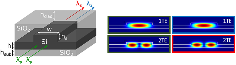
Figure 1. (Left) Sketch of the geometry of the rib waveguide (not in scale). w is the width of the waveguide, hs the height of the strip, h the height of the slab, hclad the height of the cladding over the strip and hsub the height of the substrate. The two input pump photons, at λp, are converted into signal and idler photons, respectively, at λs and λi. (Right) Simulated intensity profiles of the spatial modes excited in the rib waveguide at λ = 1.55 μm. The color code of the boxes refers to the arrow colors used in the left panel and indicates a 1221 modal combination.
In order to compare the effect of different modal combinations on fjqlm, we report in Table 1 the normalized mode field overlap and the corresponding normalized efficiency for various modal combinations in a rib waveguide with w = 2 μm, h = 300 nm, hs = 190 nm, hclad = 900 nm, and hsub = 2 μm [see Figure 1 (left) the meaning of the different parameters]. and have been calculated with all the modes at a similar wavelength of 1.55 μm. It is observed in Table 1 that the intra-modal phase-matching yields higher efficiency with respect to inter-modal phase-matching, as expected. In addition, the higher the mode order involved, the lower the efficiency of the process. Thus, the 1221 and 1122 combinations are the most suitable for inter-modal FWM. The lower efficiency of the inter-modal combinations with respect to the 1111 combination is mainly due to the spatial profile mismatch between the modes rather than to the larger effective area of the involved modes. In fact, the intra-modal combinations with higher order modes, and therefore with larger mode area, have efficiencies close to the 1111 combination.
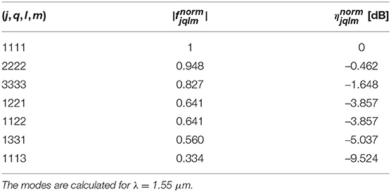
Table 1. Normalized mode field overlap and normalized efficiency for various TE modal combinations (j, q, l, m) in a rib waveguide with w = 2 μm, h = 300 nm, hs = 190 nm, hclad = 900 nm and hsub = 2 μm [see Figure 1 (left) for the meaning of the parameters].
Another critical parameter in determining the FWM generation efficiency is the waveguide width. In Table 2, we report the width dependence of and for the two modal combinations that are more efficient for both the inter-modal and intra-modal case, i.e., 1221TE and 1111TE. It can be observed that the efficiency drops by increasing the waveguide width. Intra-modal FWM in a single mode waveguide with w = 0.5 μm is much more efficient than the inter-modal phase-matching. However, propagation losses are not taken into account in this analysis. Wider multimode waveguides are expected to experience lower propagation losses than narrower single mode waveguides, due to the higher confinement of the modes in wide waveguides.
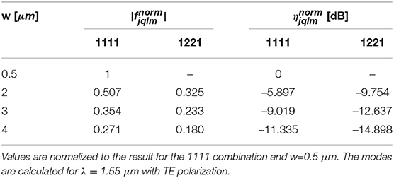
Table 2. Normalized mode field overlap and normalized efficiency for various waveguide widths and h = 300 nm, hs = 190 nm, hclad = 900 nm and hsub = 2 μm [see Figure 1 (left) for the meaning of the parameters].
Despite the lower efficiency, the inter-modal FWM allows for a large FWM generation bandwidth. Figure 2 shows the idler wavelength as a function of the waveguide width for inter-modal and intra-modal phase-matching. Here, the 1221TE inter-modal combination in a rib waveguide (orange) is compared with the 1111TE intra-modal FWM in a channel single mode waveguide (blue). The wavelength of the idler generated via inter-modal FWM spans from 1,225 to 1,510 nm, while the intra-modal FWM is phase matched only between 1,170 and 1,370 nm.
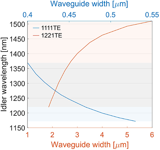
Figure 2. Phase matched idler wavelength as a function of the waveguide width. The blue line refers to the intra-modal 1111TE FWM in a single mode channel waveguide with 243 nm height. The orange line refers to the inter-modal 1221TE FWM in a rib waveguide with h = 300 nm, hs = 190 nm, hclad = 900 nm and hsub = 2 μm.
Multimode waveguides are also more fabrication tolerant than narrow single mode waveguides. Moreover, 400 nm wide channel waveguides show more than 3 dB/cm of propagation losses [25]; these losses increase for wavelengths longer than 1,700 nm. On the contrary, multimode waveguides have negligible propagation losses from 1,200 to 2,000 nm [26]. Therefore, multimode rib waveguides are the best candidate for broadband operation from 1,200 to 2,000 nm. Let us note that in our comparison we used the channel waveguide for the intra-modal FWM, since with the rib geometry it was not possible to achieve the intra-modal phase-matching. This further demonstrates the flexibility of the inter-modal process, which can be obtained with both rib and channel waveguides [6].
Finally, inter-modal FWM is characterized by discrete band phase-matching [6]. Here we mean that the phase-matching condition is achieved for a narrow region of wavelengths around the phase matched wavelength. This discrete band is useful for the generation of quantum states of light without spectral filtering [18].
3. Chip Design and Set-Up
The waveguides for inter-modal FWM generation have the cross-section shown in Figure 1 (left). They are fabricated on a SOI 6' wafer with a rib waveguide geometry. Referring to the parameters defined in Figure 1 (left), they are characterized by h = 300 nm, hs = 190 nm, hclad = 900 nm and hsub = 3 μm. Different waveguides were fabricated with different widths (range 1–4 μm), such that FWM generation in different spectral regions was possible. The multimode waveguides are then integrated in a photonic chip (Figure 3). The design of the photonic chip is aimed at exciting the different modes that participate in the FWM process in the multimode waveguide and to selectively route the desired idler and signal photons to the output. The first critical component is therefore the coupler which has to couple to or to extract from the multimode waveguide the desired low/high order mode. To this scope, we use asymmetric directional couplers (ADCs) [18].
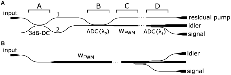
Figure 3. Schematic design of the chip for inter-modal FWM. (A) Design of the chip used for an inter-modal combination of the type 1aa1. The various functional chip parts are labeled with capital letters (A,B,C,D). 3dB-DC refers to a 3 dB coupler and ADC to an asymmetric directional coupler. wFWM indicates the multimode waveguide width. (B) Design of the chip used for an inter-modal combination of the type 11aa.
Let us go through the chip shown in Figure 3A which is designed to work with an inter-modal combination involving one pump photon and the idler photon on the first order mode and the other pump photon and the signal photon on higher order modes. This inter-modal FWM corresponds to a combination 1aa1, where a is the order of the high order mode (e.g., 1221). The pump photons are injected into the input port which is tapered from a width of 3.7 μm to a waveguide width of 0.6 μm, with a tapering length of 350 μm. In the output ports the tapering length is larger than 800 μm. This is done to maximize the coupling with the lensed fibers used to inject and extract the photons. The input waveguide is followed by a 3 dB directional coupler (DC), stage A in Figure 3, in order to split the pump in two parts. Half of the pump power (routed to the cross output port of the DC) propagates along the direction indicated by 2 in Figure 3. Here, the waveguide width starts to adiabatically widen. Therefore, half of the pump power is used to excite the first order mode of the multimode waveguide. The other half (routed to the bar port of the DC and routed to the direction indicated by 1 in Figure 3) is used to excite the higher order mode of the multimode waveguide through an ADC. This is shown in stage B of the figure. Therefore, in stage B the pump photons are propagating half on the first order and half on the high order mode. The waveguide in B continues to widen up to the desired width wFWM to achieve the required phase-matching for the inter-modal FWM. In stage C, idler and signal photons generation occurs. The length of the stage C is 1.48 cm when wFWM = 4 μm, while it is 1.5 cm for all the other values of wFWM. The last part of the chip (stage D in Figure 3) is used to separate the signal and the idler photons. Since the signal has been generated on a higher order mode, it can be extracted by using another ADC. Finally, three output ports terminate the chip. One port has the residual pump photons. The other port (output facet of the main waveguide) outputs the idler photons and the remaining pump photons (both on the fundamental mode of the multimode waveguides). The third and last port allows exiting the signal photons. Depending on the width of the multimode waveguide, different idler and signal wavelengths are generated. Thus, each ADC has been designed to optimize the coupling of the specific wavelength to the desired waveguide mode. ADCs, however, are broadband devices, thus they are tolerant to deviations from the expected target wavelength.
The ADCs have been designed based on finite element method (FEM) simulations. In Figure 4 are reported the cross-sections of the 3dB-DC and ADC (subfigure a and b respectively) and the simulated light field with λ = 1.55μm for the 3dB-DC (c) and for the 2TE mode converter ADC (d). For the ADC, the single mode waveguide is w1, while w2 is the multimode waveguide. Lcoupl is the length of the straight waveguide, where the majority of the coupling occurs. However, the simulation takes into account also the coupling due to the waveguide bends. The stages A and B in Figure 3A are common to all the devices for the 1221TE excitation. The parameters for the 3dB-DC, with 1.55 μm wavelength, are w1 = w2 = gap = 0.6μm and Lcoupl = 20.269μm. For the ADC coupling the 2TE mode, with 1.55 μm wavelength, the parameters are w1 = gap = 0.6 μm, w2 = 1.489μm, and Lcoupl = 75.613 μm.
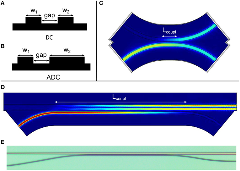
Figure 4. (A) Cross-section for the 3dB-DC. (B) Cross-section for the ADC. (C) FEM simulation of the 3dB-DC at 1.55 μm wavelength, with w1 = w2 = gap = 0.6 μm, Lcoupl = 20.269 μm. (D) FEM simulation of the ADC for the 2TE mode coupling at 1.55 μm wavelength, with w1 = gap = 0.6 μm, w2 = 1.489 μm, Lcoupl = 75.613 μm. (E) Optical image of the fabricated ADC. This ADC corresponds to the one simulated in (D).
Measurements on the fabricated chips show that the 3dB-DC has an efficiency of 0.58 and that the ADC has a coupling efficiency to the desired mode of 0.92, both measured at 1.55 μm. From the measured pump power at the residual pump output, we estimated the pump power effectively propagating in the multimode waveguide. This is 96% of the total waveguide coupled power.
Regarding the output coupler (stage D), we report, as an example, the geometrical parameters for the 1221TE inter-modal combination in the waveguide with wFWM = 4μm: w1 = gap = 0.6 μm, w2 = 1.505μm, and Lcoupl = 61.357 μm.
The propagation losses of the device are negligible, thanks to the large multimode waveguide. The coupling losses at the input and output facets are 6.0(5) dB.
Figure 3B shows a slightly different chip design used for the inter-modal combination of the type 11ab (e.g., 1122).
Two different setups have been used for the measurements. The first is shown in Figure 5A. A pulsed laser with 1,550 nm wavelength, 40 ps pulse width and 100 MHz repetition rate is used as the pump. In stimulated FWM measurements, the pump is mixed with a tunable continuous wave (CW) laser by a beam splitter and, then, they are both coupled to the same lensed fiber. This fiber couples the pump and the seed signals to the input port of the chip. Another lensed fiber is used at the output of the chip to collect the generated photons. The output fiber is then connected to a monochromator interfaced to an InGaAs SPAD (single photon avalanche detector) for spontaneous FWM experiments or to an optical spectrum analyzer (OSA) for stimulated FWM experiments. The monochromator has been realized in-house, with a grating in a double pass configuration. The InGaAs SPAD has a minimum detectable power of 1 fW and 105 dynamic range. This large dynamic range is achieved by gating the measurement with the pump laser trigger. The monochromator is limited to the spectral window 1,200–1,700 nm. Note that the position of the tapered fibers is controlled by means of two XYZ—nanopositioning stages with piezo controllers.
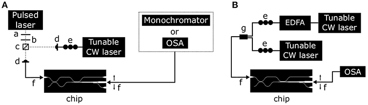
Figure 5. (A) Setup for FWM experiments with a pulsed pump laser. The pump passes through a half wave plate (a), a quarter wave plate (b) and is mixed via a free space beam splitter (c) with a CW laser used as the seed. The CW laser is polarized controlled with a fiber polarization stage (e). The two lasers are then coupled via a collimator (d) into a same lensed fiber (f). This fiber inputs the pump and the seed into the chip. Another tapered lensed fiber is used to collect the output photons. The collected photons are analyzed with a monochromator or an OSA (optical spectrum analyzer). (B) Setup for FWM experiments with a CW pump. The CW pump is amplified with an EDFA. Then it is mixed via a fiber beam splitter (g) with the CW seed.
The second setup, shown in Figure 5B, uses a continuous wave CW laser amplified by an erbium doped fiber amplifier (EDFA) for the pump. In this setup, the pump and the CW seed are mixed via a fiber beam splitter and injected into the same lensed fiber. This second set-up allows changing the pump wavelength.
FWM measurements have been performed both with a pulsed pump and a CW pump. The pulsed pump is used especially with the spontaneous FWM process where no seed is necessary. In fact, by triggering the detector with the pump pulse it is possible to reduce the measurement noise. In addition, the pulsed pump provides much higher peak intensities than the CW pump. On the other side, the CW laser allows to change the pump wavelength, investigating more accurately the bandwidth of the FWM process.
4. Results
4.1. Pulsed Pump
The set-up used for the pulsed measurement is reported in Figure 5A. With this experimental configuration we explored different inter-modal combinations, showing the waveguide width dependence of the FWM. The pump is fixed at 1,550 nm. Notice that the measurements we will show are affected by spurious peaks due to the OSA or the monochromator, which are highlighted in gray in the plots. The spectra are also affected by peaks coming from Raman scattering in the fibers or in the silicon waveguide. Indeed, at 1,434.5 nm we have the anti-Stokes Raman peak of the crystalline silicon and at 1,475 nm we have the anti-Stokes Raman peak occurring in the input silica fiber. We will use these peaks as an internal wavelength calibration.
In Figure 6 the 1221TE multimodal phase-matching combination is analyzed for different multimode waveguide widths. We report data of the spontaneous FWM process. The chip is the one whose design is shown in Figure 6A. We show the spectra of the generated idler in Figure 6A. The on-chip pump peak power is divided in 1 W on the first mode and in 0.7 W on the second mode. As the width of the multimode waveguide is reduced, the idler is generated at shorter wavelengths, see in Figure 6B. This figure also shows that the generated signal wavelength exceed 2 μm, demonstrating that with multimodal phase-matching it is possible to generate photons in the MIR. The measured (black dots) and simulated (blue full line) idler wavelengths have the same waveguide width dependence with a slight mismatch due to fabrication imperfections. In fact, if we assume a thinner stripe height hs = 170 nm, the simulated phase matched wavelengths (dashed lines) match the measured values.
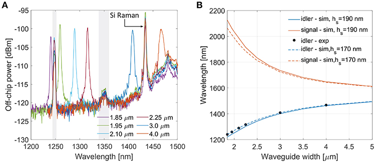
Figure 6. (A) Spectra of the generated idler for the 1221TE inter-modal combination in a spontaneous FWM experiment. Different waveguide widths are considered (width values in the legend). The peak at 1,434 nm is the anti-Stokes Raman from silicon. The broad peak at 1,475 nm is the anti-Stokes Raman peak due to the silica input fiber. The gray boxes highlight peaks due to ghosts in the grating monochnromator. (B) Simulated and measured idler and signal phase matched wavelengths as a function of the waveguide width. The experimental idler wavelengths are shown by black dots, errors are within the dot sizes. Two simulation results are shown with hs = 190 nm (full blue line) and with hs = 170 nm (dashed blue line).
Stimulated FWM experiments with the 1221TE combination has been also performed. A multimode waveguide width of 4 μm has been used, which yields an idler phase matched wavelength at 1,468.5 nm. Therefore, a seed at 1,468.5 nm was coupled into the chip and signal photons were generated at 1641.1 nm. The measured stimulated FWM spectrum is shown in Figure 7: this spectrum has been measured at the signal port of the device (see Figure 3). In Figure 7 we note a weak signal peak in the expected wavelength rage (see inset). The on-chip peak pump power was 1 W on the first order mode and 0.7 W on the second order mode. The on-chip CW seed idler power on the first order mode was 2.420(5) μW and the generated signal peak power (on-chip) was 140(5) nW. It has to be noticed that the signal power has been calculated by integrating the power over its bandwidth. If we compute the conversion efficiency as the ratio between the peak signal power and the CW seed idler power we find –12.4(2) dB1.
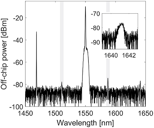
Figure 7. Stimulated inter-modal FWM for the 1221TE combination. The waveguide width is 4 μm. Spectrum measured at the signal port (see Figure 3). The idler CW seed is at 1,468.5 nm. The signal is generated at 1,641.1 nm. The gray boxes highlight the spurious peaks. In the inset we show the generated signal spectrum. The OSA is here used.
Figure 8 shows the spontaneous FWM spectra for the 1331TE phase-matching combination and different multimode waveguide widths. The working principle of the chip is the same as for the 1221TE combination, with the only difference that the ADC are designed for the third order mode for the signal photons. The idler photons are generated on the first order mode. The spectra shown in Figure 8 report the generated idler for a waveguide width of 3.5 μm at λi = 1, 257 nm and for w = 3.65 μm at λi = 1, 280 nm. Also for the 1331TE the idler wavelength changes depending on the waveguide width. The coupled pump power is the same of the 1221TE case. The idler power of the 1331TE combination is lower by 1.8(2) dB with respect to the idler from the 1221TE combination with similar waveguide width (namely 3 μm and 4 μm). This lower efficiency is close to the simulated value in Table 1, where the 1331TE combination is predicted to be less efficient than the 1221TE by about 1.2 dB. Notice that in Table 1 the waveguide width considered is 2 μm.
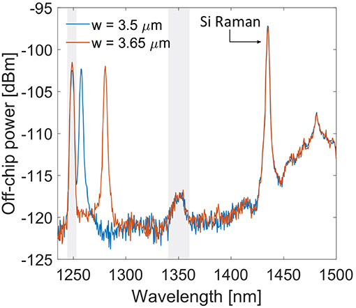
Figure 8. Spectra of the generated idler for the 1331TE inter-modal phase-matching combination in spontaneous FWM. Different waveguide widths are considered (width values in legend). The peak at 1,434 nm is the anti-Stokes Raman from silicon. The broad peak at 1,475 nm is the anti-Stokes Raman due to the silica input fiber. The gray boxes highlight spurious peaks.
Figure 9 shows the spontaneous FWM for the 1122TE phase-matching combination. Here the chip design in Figure 3B was used. The multimode waveguide is 6 μm wide. For the 1122TE phase-matching combination the efficiency is lower than for the 1221TE combination, as shown in Table 2. Due to the large waveguide width and the fact that the pump has to be coupled to the fundamental mode only, the coupling of the pump is easy. On the other hand, generated signal and idler photons have to be extracted from the multimode waveguide thorough the ADC couplers. Specifically, the generated idler photons have to be measured at the idler port (see the chip design in Figure 3B). Figure 9 shows the spectra of the generated idler. The blue line refers to the spectrum measured at the residual port, while the orange line to the spectrum measured at the idler port. The idler port spectrum is less affected by pump and Raman noise, since these two signals propagate on the first order mode. This shows a further advantage of the proposed chip design, which allows a better pump and Raman noise rejection with respect to intra-modal FWM. The on-chip peak pump power used is 1.7(1) W and the idler photons are generated at 1,271 nm.
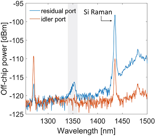
Figure 9. Spectra of the generated idler for the spontaneous FWM with an inter-modal combination 1122TE. The waveguide width used is 6 μm. The idler spectrum has been measured at the residual (blue) and idler (orange) ports. The peak at 1,434 nm is the anti-Stokes Raman from silicon. The broad peak at 1,475 nm is the anti-Stokes Raman due to the silica input fiber. The gray boxes highlight the spurious peaks.
We summarize in Table 3 the measured and simulated phase matched idler wavelengths for various inter-modal phase-matching combinations and different waveguide widths. A good agreement between experiments and simulations is achieved with the nominal multimode waveguide parameters. Furthermore, it can be seen that a better agreement between the experiment and the simulation can be achieved with a thinner hs = 170 nm than the nominal 190 nm. This shows that inter-modal FWM can be potentially used as a tool for the not invasive characterization of the waveguide cross section of multimode waveguides.
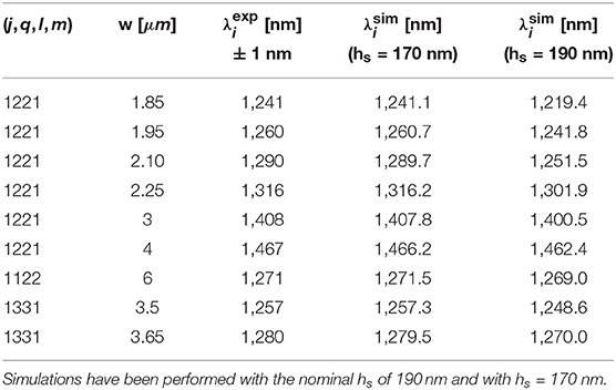
Table 3. Measured () and simulated () phase matched idler wavelengths for different modal combinations (j,q,l,m) and waveguide widths.
Finally, we have shown that the generation of idler photons in the spectral region about 1,260–1,270 nm can be achieved with several inter-modal phase-matching combinations. The simulated efficiencies reported in Tables 1, 2 indicate that the most efficient inter-modal combination is the 1221TE combination, which exhibits the highest efficiency due to a large mode field overlap and a narrow required waveguide width. Therefore, in the following we will use the 1221 inter-modal phase-matching combination for CW experiments.
4.2. CW Pump
The set-up used with the CW pump is shown in Figure 5B, the signal is here recorded with an OSA. We used a 4 μm waveguide with the 1221TE inter-modal phase-matching combination (Figure 3A). In stimulated FWM experiments, the seed is at the phase matched idler wavelength of 1,468.8 nm and the generated signal photons at 1,640.7 nm. Figure 10A shows the stimulated FWM spectrum measured at the signal port of the chip. The on-chip pump power is 35(2) mW on the first mode and 22(2) mW on the second mode. The on-chip seed power on the first order mode is 20(5) μW and the generated signal power is 6(1) ×102 pW. The conversion efficiency is –45 dB. The efficiency is lower with respect to the value measured with pulsed pump due to the lower peak pump power. The baseline noise is due to the Fabry-Perot interference occurring in the multimode waveguide. By moving the seed wavelength we measured the bandwidth of the FWM process. This is reported in Figure 10B where the generated signal spectra are reported for different seed idler wavelengths. The pump wavelength is fixed at 1,550 nm. It is observed that the intensity of the generated signal peak depends on the seed idler wavelength. A simulation of the FWM generation efficiency (Equation 4) is also added as the black dashed line. The simulation has been carried out by solving the coupled wave equations of FWM [6] using the pump and seed powers used in the experiment. The simulation fits well the experiment, with a 3-dB bandwidth of 11(1) nm.
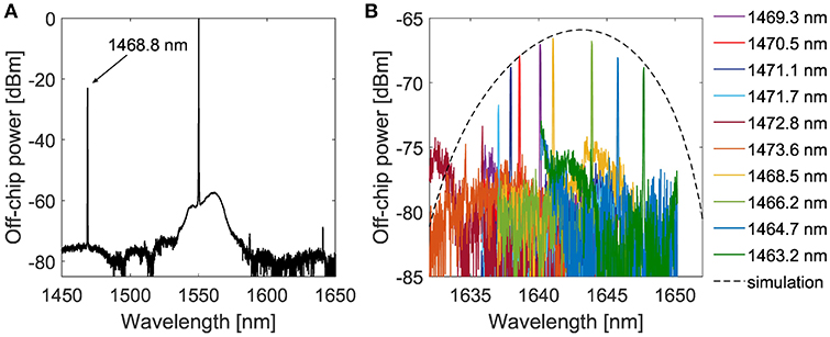
Figure 10. Stimulated inter-modal FWM with 1221TE phase-matching combination in a 4 μm wide waveguide. The pump is CW at 1,550 nm. (A) Stimulated inter-modal FWM spectrum. The gray boxes highlight the spurious peaks. The seed is at 1468.8 nm. (B) Signal spectra as a function of the seed wavelength (in legend). The black dashed line refers to the simulated FWM efficiency.
The large bandwidth makes the inter-modal process suitable for all optical operations within the WDM framework. In order to span an even larger bandwidth it is possible to move the pump wavelength instead of the idler wavelength. Figure 11A shows the measured signal wavelength as a function of the pump wavelength, when the seed wavelength is fixed at 1,467 nm. We show that the signal wavelength shift linearly with the pump wavelength. A linear fit (y = ax+b) yields a = 2.3, with (2.2, 2.5) 95% confidence bounds. This means that the signal wavelength moves by 2.3 nm per nm variation of the pump wavelength. Figure 11B shows the signal generation bandwidth. Here the experimental points correspond to the spectra in Figure 11A. The points have been fitted with a Gaussian function, finding a full width at half maximum (FWHM) of 21 nm, with (11, 30 nm) 95% confidence bounds. The data at 1,635 and 1,640 nm have been excluded from the fit being largely affected by Fabry-Perot interference. The large measured bandwidth suggests that the inter-modal FWM can be used as a broadband wavelength converter by varying the pump wavelength, too. In fact, with fixed pump wavelength and by varying the seed wavelength, the 3-dB bandwidth is limited to 11 nm, as shown in Figure 10B.
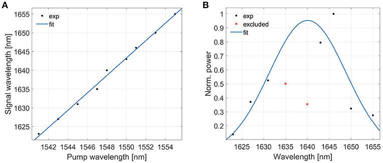
Figure 11. (A) Signal wavelength as a function of the pump wavelength for stimulated inter-modal FWM with 1221TE phase-matching combination in a 4 μm wide waveguide. The pump is CW. The seed idler wavelength is fixed at 1,467 nm. The black dots are the experimental points. The line refers to a linear fit of the data. (B) Normalized signal generated power as a function of the signal wavelength. In black are the experimental points used for the gaussian fit of the data. In red the experimental points excluded from the fit.
5. Conclusions
In this work we analysed the inter-modal FWM process in an integrated chip whose design is optimized for handling the different waveguide modes which are involved in the non-linear process. We initially described the dependence of the inter-modal FWM efficiency on the modal combination and on the waveguide width. We show that the inter-modal phase-matching features a high degree of flexibility at the expenses of the efficiency with respect to the intra-modal phase-matching. In fact, it can be phasematched over a broad spectral range (1,200–1,500 nm for the idler wavelength with 1,550 nm pump wavelength). We experimentally demonstrate several inter-modal combinations (1221TE, 1122TE, 1331TE) using a suitable chip design for each of them. The main element in the design is the asymmetric mode coupler which allows injecting and extracting specific modes from the multimode waveguide. We also suggest that the inter-modal FWM can be used as a tool for the characterization of the geometrical parameters of the multimode waveguide thanks to the sensibility of the phase-matching wavelengths on the actual multimode cross-section.
We focused on the 1221TE combination, that proved to be the more efficient for inter-modal FWM. We demonstrated a high control with the waveguide geometry, tuning its phase matched idler wavelength between 1,240 and 1,470 nm by changing the waveguide width. We measured a conversion efficiency of –12.4 dB from a seed at 1,468.5 nm to a signal at 1,641.1 nm, with a 3-dB bandwidth of 11 nm. Moreover, we proved also a high tunability of the generated signal wavelength when the seed is kept at a fixed wavelength and the pump wavelength is changed. We measured a 3-dB bandwidth of 21 nm. This shows that the inter-modal FWM can be used for high tunable and selective all optical wavelength operation, as required in the WDM framework.
The inter-modal FWM is characterized by broadband and large spectral translation, also accessing the MIR spectrum. By using the design here proposed, it is possible to generate correlated pairs of photons with tunable spectral separation. The flexibility of the inter-modal FWM together with the broadband ADCs allow separating the signal and idler photons directly on the chip, improving the pump and Raman noise rejection.
Data Availability
The datasets generated for this study are available on request to the corresponding author.
Author Contributions
SS wrote the paper, developed the theory and the simulations, designed the chip, and carried out the stimulated FWM measurements. MF made the spontaneous FWM measurements and characterized the DCs and ADCs. MB, MG, and GP fabricated the samples. LP supervised the work.
Funding
This work was supported by the Siquro project (Bando grandi progetti, Provincia Autonoma di Trento, 2012) and by the NEMO project (PRIN 2015KEZNYM supported by MIUR).
Conflict of Interest Statement
The authors declare that the research was conducted in the absence of any commercial or financial relationships that could be construed as a potential conflict of interest.
Supplementary Material
The Supplementary Material for this article can be found online at: https://www.frontiersin.org/articles/10.3389/fphy.2019.00128/full#supplementary-material
Footnotes
1. ^For a more detailed analysis of the conversion efficiency calculation see the Supplementary Materials.
References
1. Liu A, Liao L, Chetrit Y, Basak J, Nguyen H, Rubin D, et al. Wavelength division multiplexing based photonic integrated circuits on silicon-on-insulator platform. IEEE J Select Topics Quant Electr. (2010) 16:23–32. doi: 10.1109/JSTQE.2009.2033454
2. Dai D, Wang J, He S. Silicon multimode photonic integrated devices for on-chip mode-division-multiplexed optical interconnects. Prog Electromagn Res. (2013) 143:773–819. doi: 10.2528/PIER13111003
3. Pourbeyram H, Nazemosadat E, Mafi A. Detailed investigation of intermodal four-wave mixing in SMF-28: blue-red generation from green. Opt Express. (2015) 23:14487–500. doi: 10.1364/OE.23.014487
4. Ding Y, Xu J, Ou H, Peucheret C. Mode-selective wavelength conversion based on four-wave mixing in a multimode silicon waveguide. Opt Express. (2014) 22:127–35. doi: 10.1364/OE.22.000127
5. Pan W, Jin Q, Li X, Gao S. All-optical wavelength conversion for mode-division multiplexing signals using four-wave mixing in a dual-mode fiber. JOSA B. (2015) 32:2417–24. doi: 10.1364/JOSAB.32.002417
6. Signorini S, Mancinelli M, Borghi M, Bernard M, Ghulinyan M, Pucker G, et al. Intermodal four-wave mixing in silicon waveguides. Photon Res. (2018) 6:805–14. doi: 10.1364/PRJ.6.000805
7. Lacava C, Ettabib MA, Bucio TD, Sharp G, Khokhar AZ, Jung Y, et al. Intermodal Bragg-Scattering Four Wave Mixing in Silicon Waveguides. J Lightwave Techn. (2019) 67:1680–5. doi: 10.1109/JLT.2019.2901401
8. Lacava C, Bucio TD, Khokhar AZ, Horak P, Jung Y, Gardes FY, et al. Intermodal frequency generation in silicon-rich silicon nitride waveguides. Photon Res. (2019) 7:615–21. doi: 10.1364/PRJ.7.000615
9. Zhang J, Alonso-Ramos C, Vivien L, He S, Cassan E. Self-adaptive waveguide boundary for wideband multi-mode four-wave mixing. arXiv [Preprint] arXiv:190206170 (2019).
10. Hu T, Dong B, Luo X, Liow TY, Song J, Lee C, et al. Silicon photonic platforms for mid-infrared applications. Photon Res. (2017) 5:417–30. doi: 10.1364/PRJ.5.000417
11. Rottwitt K, Koefoed J, Christensen E. Photon-pair sources based on intermodal four-wave mixing in few-mode fibers. Fibers. (2018) 6:32. doi: 10.3390/fib6020032
12. Crowder J, Smith S, Vass A, Keddie J. Infrared methods for gas detection. In: A. Krier, editor. Mid-Infrared Semiconductor Optoelectronics. London, UK: Springer (2006). p. 595–613. doi: 10.1007/1-84628-209-8-18
13. Lin H, Luo Z, Gu T, Kimerling LC, Wada K, Agarwal A, et al. Mid-infrared integrated photonics on silicon: a perspective. Nanophotonics. (2017) 7:393–420. doi: 10.1515/nanoph-2017-0085
14. Mancinelli M, Trenti A, Piccione S, Fontana G, Dam JS, Tidemand-Lichtenberg P, et al. Mid-infrared coincidence measurements on twin photons at room temperature. Nat Commun. (2017) 8:15184. doi: 10.1038/ncomms15184
15. Silverstone JW, Bonneau D, O'Brien JL, Thompson MG. Silicon quantum photonics. IEEE J Select Topics Quant Electr. (2016) 22:390–402. doi: 10.1109/JSTQE.2016.2573218
16. Moreau PA, Sabines-Chesterking J, Whittaker R, Joshi SK, Birchall PM, McMillan A, et al. Demonstrating an absolute quantum advantage in direct absorption measurement. Sci Rep. (2017) 7:6256. doi: 10.1038/s41598-017-06545-w
17. Temporao G, Zibinden H, Tanzilli S, Gisin N, Aellen T, Giovannini M, et al. Feasibility study of free-space quantum key distribution in the mid-infrared. Quant Inform Computat. (2008) 8:1–11.
18. Signorini S, Piccione S, Ghulinyan M, Pucker G, Pavesi L. Are on-chip heralded single photon sources possible by intermodal four wave mixing in silicon waveguides? In: Quantum Photonic Devices 2018, Vol. 10733. International Society for Optics and Photonics (2018). p. 107330G. doi: 10.1117/12.2320956
19. Feng LT, Zhang M, Xiong X, Chen Y, Wu H, Li M, et al. On-chip transverse-mode entangled photon pair source. NPJ Quant Inform. (2019) 5:2. doi: 10.1038/s41534-018-0121-z
21. Borghi M, Castellan C, Signorini S, Trenti A, Pavesi L. Nonlinear silicon photonics. J Opt. (2017) 19:093002. doi: 10.1088/2040-8986/aa7a6d
22. Xiao Y, Essiambre RJ, Desgroseilliers M, Tulino AM, Ryf R, Mumtaz S, et al. Theory of intermodal four-wave mixing with random linear mode coupling in few-mode fibers. Opt Express. (2014) 22:32039–59. doi: 10.1364/OE.22.032039
23. Foster MA, Turner AC, Salem R, Lipson M, Gaeta AL. Broad-band continuous-wave parametric wavelength conversion in silicon nanowaveguides. Opt Express. (2007) 15:12949–58. doi: 10.1364/OE.15.012949
24. Liu X, Kuyken B, Roelkens G, Baets R, Osgood Jr RM, Green WM. Bridging the mid-infrared-to-telecom gap with silicon nanophotonic spectral translation. Nat Photon. (2012) 6:667. doi: 10.1038/nphoton.2012.221
25. Vlasov YA, McNab SJ. Losses in single-mode silicon-on-insulator strip waveguides and bends. Opt Express. (2004) 12:1622–31. doi: 10.1364/OPEX.12.001622
Keywords: four wave mixing, inter-modal four wave mixing, silicon photonics, waveguide modes, wavelength conversion
Citation: Signorini S, Finazzer M, Bernard M, Ghulinyan M, Pucker G and Pavesi L (2019) Silicon Photonics Chip for Inter-modal Four Wave Mixing on a Broad Wavelength Range. Front. Phys. 7:128. doi: 10.3389/fphy.2019.00128
Received: 13 June 2019; Accepted: 26 August 2019;
Published: 13 September 2019.
Edited by:
Shinichi Saito, University of Southampton, United KingdomReviewed by:
Isao Tomita, National Institute of Technology, Gifu College, JapanKoji Yamada, National Institute of Advanced Industrial Science and Technology (AIST), Japan
Copyright © 2019 Signorini, Finazzer, Bernard, Ghulinyan, Pucker and Pavesi. This is an open-access article distributed under the terms of the Creative Commons Attribution License (CC BY). The use, distribution or reproduction in other forums is permitted, provided the original author(s) and the copyright owner(s) are credited and that the original publication in this journal is cited, in accordance with accepted academic practice. No use, distribution or reproduction is permitted which does not comply with these terms.
*Correspondence: Stefano Signorini, c3RlZmFuby5zaWdub3JpbmktMUB1bml0bi5pdA==