 Kunji Chen
 Zewen Lin
 Pengzhan Zhang
 Rui Huang2
 Hengping Dong
- 1School of Electronic Science and Engineering, and Collaborative Innovation Center of Advanced Microstructures, Nanjing University, Nanjing, China
- 2Department of Physics and Electronic Engineering, Hanshan Normal University, Chaozhou, China
- 3Jinling Institute of Technology, College of Electronic and Information Engineering, Nanjing, China
- 4Taizhou Institute of Science and Technology, Nanjing University of Science and Technology, Taizhou, China
Silicon oxynitride films are one kind of important gate dielectric materials for applications in the fabrication of silicon CMOS integrated circuits (ICs), which have been widely and deeply studied. However, with the significant demand of the technologies for Si-based monolithic optoelectronic ICs, the research efforts on the optoelectronic applications of these materials have been continually increasing, particularly in the study of light emission properties and recombination mechanisms. In this paper, we first briefly outline the present photoluminescence (PL) mechanisms in amorphous silicon oxynitride (a-SiOxNy) films. Since, the PL properties and recombination processes are affected by both structural disorder and chemical disorder, the PL mechanism has been still unclear and even controversial until now. Among these various PL recombination models, the band tail states and defect state models have gained general consensus. Recently, a N-Si-O bond defect model has been reported, which depends on relative atom concentration of oxygen and nitrogen in the silicon oxynitride materials. It has been revealed that oxygen bonding plays a key role, not only in reducing the structural disorder, but also in creating N-Si-O (Nx) defect states in the band gap. The characteristics of two models, namely band tail and N-Si-O bond defects, have been discussed in detail. Finally, it has been shown that by controlling the chemical composition of these non-stoichiometric silicon oxynitride materials, the optical and electronic properties can be improved.
Introduction
A family of silicon based silicon oxide and nitride is traditional and important electronic and optical films, which have been widely applied in the fields of microelectronic and optoelectronic devices. Among these materials, the structures and properties of amorphous silicon oxynitride (a-SiOxNy) films including oxygen-rich silicon oxynitride (O-type a-SiOxNy) and nitride-rich silicon oxynitride (N-type a-SiOxNy), are very different from those of stoichiometric SiO2 and Si3N4. During the first decade, after the first publications by Fukuda et al. [1] and Hwang et al. [2] in 1990, silicon oxynitride films have been extensively studied as a replacement for the conventional SiO2 gate dielectric. In contrast to SiO2, this kind of materials has higher dielectric constants and excellent diffusion-limiting properties, which can therefore suppress the penetration of boron from the poly-Si gate, as well as enhance the reliability [3–5]. On the other hand, incorporation of nitrogen in Si/SiO2 interfaces can improve both electronic and optical properties [6], which will be discussed in detail in section Role of oxygen bonding and N-Si-O bonding defects.
A large number of techniques have been proposed and evaluated to engineer the concentration and distribution of nitrogen and oxygen in the silicon oxynitride films. Among them, the physical or chemical vapor deposition with various nitrogen based reaction sources, such as N2O [7–10], NO [11, 12], and NH3 [13–15] etc., can be used to directly grow a-SiOxNy films. Besides, the nitridation treatments [thermal [16] or plasma [17–19]] can also be used to control the nitrogen concentration in the grown SiO2 films. In the meantime, many works on the characterization of structures, physical and electrical properties of silicon oxynitride films for the microelectronic applications have also been reported [12, 20–22].
On the other hand, the silicon oxynitride films have been employed, not only as an alternative gate dielectric layers for application in microelectronic devices, but also as optical materials in optoelectronic devices, such as ultraviolet transparent waveguide [23–25], microarrays of Si-based light emitters for biosensor [26], CO2 capturer [27], light emitting devices [28–30], and solar cells [31]. With the prime requirements of the technologies for integrating optoelectronic devices with silicon-based microelectronics, the research efforts on optical properties of silicon oxynitride films have been continually increasing. Among these, most research focused on the study of light emission properties and the recombination mechanism. However, even though the photoluminescence (PL) efficiency of silicon oxynitride is higher than that of other Si-based luminescent materials, it is still lower for practical application requirements. Hence, understanding the PL mechanisms in silicon oxynitride remains the key foundation for fabricating Si-based high-efficiency light emitting devices.
In this paper, we first briefly outline the present PL mechanisms of a-SiOxNy films in section PL properties and recombination mechanisms in a-SiOxNy films. Some groups reported that the PL in O-type a-SiOxNy was due to radiative recombination between localized band-tail states associated with Si-N bonds which is similar to a-SiNx [32, 33], while other groups clarified that the complete picture of PL in silicon oxynitride can be explained by the radiative recombination via both band tail states and luminescent defect states [34]. Besides, it was also suggested that the PL might arise from radiative recombination center consisting of the silicon sub-oxide bonding defects [35–37]. Among these various PL models, even though the band tail state and defect state models have gained general consensus, PL mechanisms have still been unclear and even controversial. In section Role of oxygen bonding and N-Si-O bonding defects, we analyzed the role of oxygen bonding being played in silicon oxynitride network, which not only reduced the structural disorder but also created N-Si-O (Nx) defect states in the band gap. Based on this, a N-Si-O bond defect model has been proposed in section Characteristics of band tail states and defect states dominated PL model in a-SiOxNy, which depends on relative atom concentration of oxygen and nitrogen in the silicon oxynitride materials. In section Improved optical properties in N-type a-SiNxOy films, the characteristics of two PL models, i.e., band tail and N-Si-O bond defect, have been discussed in detail. Finally, we showed that by controlling the chemical composition of this non-stoichiometric silicon oxynitride materials the optical and electronic properties can be improved. An n-a-SiNxOy/p-Si HJ LED fabricated by the standard CMOS technology has been demonstrated. Finally, the gate controlled Si MOSFET has been emphasized and discussed.
PL Properties and Recombination Mechanisms in a-SiOxNy Films
In this section, we briefly outline the present PL mechanisms in a-SiOxNy films. It is well-known that, in the non-stoichiometric a-SiOxNy materials, the PL properties are affected not only by preparation methods but also by the relative chemical composition of Si, N, and O elements. Over the last two decades, many works on study of PL mechanism were reported, but it has been still unclear and even remained ambivalent up to date. This is probably due to the difficulties of controlling and separating individual contribution made by both structural disorder and chemical disorder which are contained in this kind of material.
In the 1990s, a group at university of North Carolina, Augustine et al. [36], started the study of the visible light emission from thin films containing Si, O, N, and H. The a-SiOxNy:H samples were prepared by PECVD using SiH4 and N2O at elevated temperatures. The results of X-ray photoelectron spectra (XPS) and Fourier-transform infrared (FT-IR) spectroscopy showed that the chemical composition was dominated by silicon sub-oxide bonding with N atoms serving as a significant impurity. The broad visible PL emission was observed at room temperature. The radiative lifetime was <10 ns and the PL intensity was nearly unchanged from 80 to 300 K. The combined results suggested that N was not the radiative center in the SiOxNy matrix, but the silicon sub-oxide bonding acted as a defect state which enabled visible PL emission. Thereafter, they reported [35] the effect of the rapid thermal annealing on PL properties of a-SiOxNy:H films. It was suggested that the annealing was characterized by two processes. The first was that the Si-H and N-H bonds were broken and hydrogen effused from hydrogen clustering region, which resulted in an increase of dangling bond density. The second was the local reconstruction of Si-O and Si-N bonds. The results obtained after annealing were in agreement with the above PL characteristics, based on which PL recombination model was schematically shown in Figure 1A. Due to the local chemical bonding disorder, the density of these localized states was not smoothly decaying from the mobility edges of conduction and valence bands, as shown in Figure 1B.
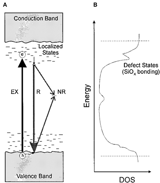
Figure 1. (A) Schematic representation of the model of geminate PL recombination through localized defect states within the band tails. Excitation is denoted by EX, radiative recombination by R, and non-radiative recombination at midgap states by NR. (B) Energy vs. density of states in the band gap. Structure is due to localized chemical bonding in the films. The mobility edges are denoted by horizontal dotted lines [Reprinted from Augustine et al. [35], with permission].
Four years later, based on above results, Price, McNeil and Irene et al. [34, 37] further characterized the luminescence center in a-SiOxNy films. The experimental results excluded the origin of PL emission from Si dangling bonds, NBOHC [38, 39] and N dangling bonds, as well as silicon nanocrystals. The recombination mechanism of a complete PL spectrum in near-stoichiometric a-SiOxNy:H films must be associated with both band tail states and defect states.
At the beginning of the 2000s, Noma et al. [40], reported that the four PL peaks appearing in the range from 2 to 5 eV had been observed in oxygen-rich a-SiOxNy:H films, deposited by PECVD using SiH4, N2O, and N2 as reaction gases. The study combining with FTIR, XPS, electron spin resonance (ESR) and scanning electron micrographs (SEM) indicated that the two peaks of 2.7 and 4.4 eV were originated from silicon homo-bonds, and the other broad peaks located around 2.6–2.9 eV were due to the Si-N bonds in the gathering regions of Si-N bonds. Furthermore, since the samples were prepared by PECVD using SiH4 gas source, a-SiOxNy:H samples contained hydrogen. In order to eliminate the effect of hydrogen, the samples were prepared by nitridation of silicon dioxide and, thus, were free of hydrogen [33]. The results of the emission spectrum, excitation spectrum and time-resolved PL (TRPL) spectrum, combined with the theoretical analysis, again confirmed that the origin of the PL with its peak in the range of 2.6–2.9 eV was from the Si-N bonds in a-SiOxNy film, and thus irrelevant to hydrogen content.
Soon afterwards, Kato et al. [32, 41, 42] further performed the research on the PL mechanism in a-SiOxNy films and a-SiNx films. The conclusion was drawn that the PL from a-SiOxNy films originated from radiative recombination between localized band-tail states associated with Si-N bonds. The experimental evidences were shown in Figures 2, 3. As shown in Figure 2A, the bandwidth of PL (ΔEPL) caused by the band-tail recombination is proportional to the width of the localized states (EU), in which the straight line passes the origin of the coordinate axes, indicating that the band-tail states are mostly induced by structural disorder. Figure 2B shows the PL peak energy (EPL) increases monotonically with an increase in Urbach edge energy EUedge in both a-SiOxNy and a-SiNx films, which means that they exhibit the same feature of band-tail recombination mechanism. The time-resolved PL (TRPL) measurements were used to analyze the recombination processes of photo-excited carriers. The results of nanosecond temporal evolution of transient PL showed that the EPL shifted as a function of specific delay time after excitation. As shown in Figures 3A,B, for both a-SiOxNy and a-SiNx, EPL first shifts to red, then to blue, and back to red again. It is also a feature of the band-tail recombination mechanism, in which three different effects are included, such as thermalization, coulomb interaction, and extent of localization of carriers, acting together to cause the shift of PL peaks.
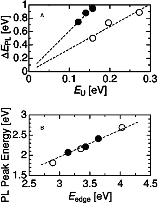
Figure 2. (A) Relation between the Urbach energy EU and the FWHM of the PL spectrum ΔEPL. Closed and open circles are for a-SiOxNy:H and a-SiNx:H, respectively. (B) Correlation between the Urbach edge energy Eedge and the PL peak energy. Closed and open circles are for a-SiOxNy:H and a-SiNx:H, respectively [Reprinted from Kato et al. [32], with permission].
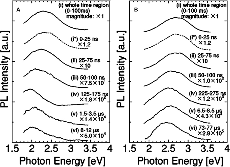
Figure 3. Typical time-resolved PL spectra excited by 5.0-eV photons, observed in a-SiOxNy:H (A) and a-SiNx:H (B). Numerals following (i)~(vi) indicate given observation periods [Reprinted from Kato et al. [32], with permission].
In the late 2000s, Tewary et al. [43] reported luminescence from controlling defect and Si nanoparticle in a stoichiometry SiO1.08N0.32 films by using CO2 laser annealing. It was found that there were two distinct peaks located at 570 and 800 nm in the irradiated areas. From the combined study of TEM and PL lifetime, it can be concluded that the visible peak with a short PL lifetime of ~10 ns was related to silicon sub-oxide defects, which was the same as that reported by Augustine et al. [36], while the infrared peak was due to exciton recombination in Si nanoparticles.
Since 2006, Huang et al. [44] have observed strong green light emission from oxidized SiNx films. The samples were fabricated by PECVD at room temperature followed by thermal or plasma oxidation at 100°C, which is different from a-SiOxNy films prepared by PECVD using N2O and SiH4 as reaction gas sources. Subsequently, they observed green-yellow electroluminescence from this kind of oxidized a-SiNx films [29, 45]. At that time, it was suggested that the light emission was due to the radiative recombination through the luminescent center related to Si-O bonds in the Si-N matrix. Based on above investigations, Dong et al. [46] further characterized the luminescent defect states. The results from measurements of FTIR and XPS verified the existence of O-Si-N bonding configuration, which acted as a new luminescent defect state in our a-SiNxOy films.
In recent years, Ruggeri et al. [47] reported that the luminescent signal in a-SiOxNy layer was affected by silicon chemical environment induced by IR annealing inside the amorphous SiON matrix. Jou et al. [48] reported PL characteristics of a-SiOxNy films, which were prepared by reactive sputtering of silicon. The PL spectra with blue and green peaks were observed. The blue and green emissions possibly arose from N related defects and O-Si-N bonding related defects, respectively.
More recently, Zhang et al. [49] and Lin et al. [30] conducted the intensive investigation on PL mechanism in a-SiNxOy films. The results of XPS and EPR, as well as PLE measurements, indicated that the oxygen atoms in SiNx matrix not only reduced the structural disorder but also created N-Si-O (Nx) defect states in the band gap. And then the PL mechanism dominated by the N-Si-O defect states was proposed, which will be discussed in detail in sections Role of oxygen bonding and N-Si-O bonding defects and Characteristics of band tail states and defect states dominated PL model in a-SiOxNy.
Role of Oxygen Bonding and N-Si-O Bonding Defects
Before discussion about the role of oxygen bonding in a-SiOxNy, we would like to very briefly summarize the role of Si/SiO2 interface region on photoelectronic properties of luminescent silicon. As mentioned above, the structures and properties of Si/SiO2 interface is a critical factor for influencing the performance of the electronic and optical devices. For the luminescent silicon, like porous silicon, silicon nanocrystals (Si-nc) and silicon quantum dots, the sharp and stable Si/SiO2 interface can passivate non-radiative defect states on the surface, and consequently provide stable light emission [6]. On the other hand, Wolkin et al. [50] observed that oxidation can also form Si=O double bonds, which act as a luminescent defect states in the Si-nc band gap and pin their emission energy. Moreover, Pavesi et al. [51] reported that radiative luminescent interface states play a key role in the optical gain of Si-nc.
For a-SiOxNy films, apart from the preparation methods and conditions, the relative atomic concentration of oxygen and nitrogen O/(O+N) is a crucial factor influencing their chemical bonding configuration and physical properties. For example, when the ratio O/(O+N) > 0.4, the nitride-like structures will be transformed into oxide-like structures and, consequently, the electronic properties will be changed in the silicon oxynitride gate dielectric layer [5]. Thereafter, for simplicity, in this paper the “O-type a-SiOxNy” film is used to denote oxygen-rich amorphous oxynitride film, and the “N-type a-SiNxOy” film refers to nitrogen-rich amorphous oxynitride film [52].
In the study on optical properties of a-SiOxNy films, it has also been found that the PL properties are dependent on the O/(O+N) ratio. As mentioned above, Kato et al. [32], Price et al. [34] and Augustine et al. [36] reported PL from the a-SiOxNy films prepared by PECVD with N2O:SiH4 reaction gases. From XPS measurements, the O/(O+N) ratio was determined in the range of 0.60–0.90, suggesting these a-SiOxNy films can be called O-type a-SiOxNy films. They believed that the PL arose either from radiative recombination between localized band-tail states associated with Si-N bonds similar to a-SiNx films or from both band-tail states and luminescent defect states, which consist of silicon sub-oxide bonding defects. However, in our previous works [44, 46, 49], the a-SiNxOy films were prepared by PECVD with NH3:SiH4:N2 reaction gases, and then subsequently oxidized in situ by oxygen plasma [53]. As the O/(O+N) ratio is able to be controlled in the range of 0.05–0.15, and these a-SiNxOy films can be called as N-type a-SiNxOy films. The origin of the PL was found to be attributed to the radiative recombination through the luminescent N-Si-O bonding defect states, which is different from band-tail states recombination model and will be discussed in section Characteristics of band tail states and defect states dominated PL model in a-SiOxNy.
In order to explain the role of oxygen bonding in the atomic structure and PL properties of a-SiNxOy films, we prepared a series of N-type a-SiNxOy samples with different reaction gas ratios R = [NH3]/[SiH4] which were listed in Table 1 [49]. It shows that for our samples, the O/(O+N) ratio was in the range of 0.07–0.13. For comparison, three kind of controlled a-SiNx films were also prepared by PECVD but without oxidation plasma treatment. The optical parameters of both series of a-SiNxOy and a-SiNx samples, such as optical band gap Eopt, Urbach tail edge EUedge, Urbach tail width EU, and PL peak energy EPL etc., were listed in Table 2. Figure 4A shows the band tail EUedge and EU as a function of R. When the R increases, the EUedge and EU increase monotonically in both a-SiNxOy and a-SiNx samples. This phenomenon resulted from the increase in short range structural disorder with increasing of atomic ratio N/Si in amorphous Si based nitride. Moreover, it is interesting to find that the degree of short range structural disorder in a-SiNxOy is smaller than that in a-SiNx. For example, at R = 2, the band tail width EU in a-SiNxOy film is equal to 0.66 eV, while EU amounts to 1.5 eV in a-SiNx film. It can be considered that since O atoms are more electronegative than N atoms, the incorporated O atoms will easily substitute N atoms to form Si-O bonds in the silicon nitride network. On the other hand, according to the chemical bonding principle, oxygen takes two-fold coordination to form Si-O bonds, whereas nitrogen takes three-fold coordination to form Si-N bonds, therefore, the Si-O bonds can relieve the internal stress, which results in smaller network disorder and narrower band tail width (EU) in our N-type a-SiNxOy samples. The data in Figure 4B is reprinted from Kato et al. [32]. They also found that the degree of the structural disorder in a-SiOxNy:H was smaller than that in a-SiNx:H and gave similar explanations.
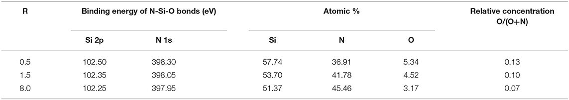
Table 1. Binding energy of N 1s and Si 2p in N-Si-O bond configurations, and Si, N, O chemical compositions of a-SiNxOy films from XPS spectra.
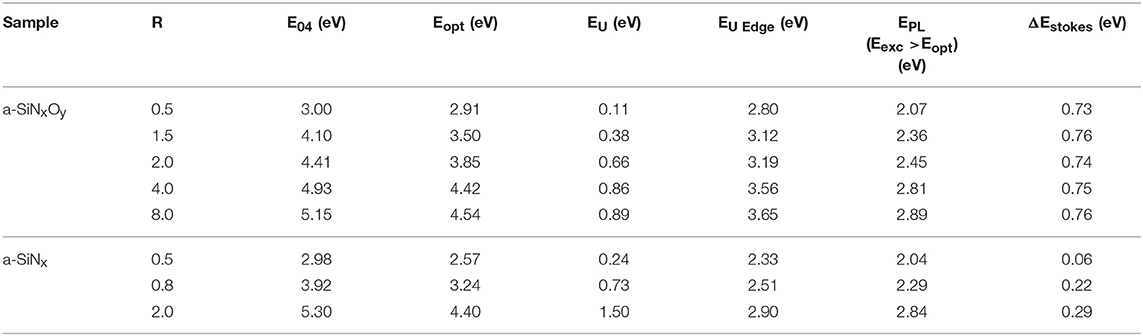
Table 2. Summary of the optical parameters and PL peak energies of two series of samples at 9 K.
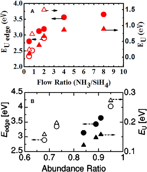
Figure 4. (A) Urbach edge energy EUedge (circles) and the Urbach energy EU (triangles) vs. flow ratio NH3/SiH4. Closed and open symbols are for a-SiNxOy and a-SiNx, respectively [After Zhang et al. [49], with permission]. (B) Urbach edge energy Eedge (circles) and the Urbach energy EU (triangles) vs. abundance ratio. Closed and open symbols are for a-SiOxNy:H and a-SiNx:H, respectively [Reprinted from Kato et al. [32], with permission].
The incorporation (or say doping) of oxygen atoms into amorphous silicon nitride networks not only reduced the band tail structural disorder, but also created N-Si-O bonding defect states in the band gap. We employed XPS and EPR measurements combining with silicon tetrahedral bonding model to verify the existence of N-Si-O bond configuration in our N-type a-SiNxOy films. By XPS measurements, the relative atomic concentration of Si, N, and O can be determined by the area integration of each binding energy peak of Si 2p, N 1s, and O 1s, respectively, which were listed in Table 1 [49]. We can see that the relative atom ratio of O and N, i.e., O/(O+N), is <0.1, which means that O atoms serve as impurities in the silicon nitride network, accordingly it can be called as N-type a-SiNxOy films.
For the study of bonding configurations in non-stoichiometric a-SiOxNy films, several literatures have been published [54–58]. Cova et al. [55] reported that, in the a-SiNxOy network, hetero-bonds (Si-N and Si-O bonds) are more preferably formed than homo-bonds (Si-Si, N-N, and O-O bonds), by reason of different bonding energies. That is to say, the bonding energies of homo-bonds [Eb(Si-Si) = 1.8 eV, Eb(N-N) = 1.6 eV, and Eb (O-O) = 1.4 eV] are weaker than those of hetero-bonds [Eb(Si-N) = 3.5 eV and Eb (Si-O) = 3.8 eV]. From XPS measurements, based on analysis of the Si 2p spectra, the results of the binding energy shift, which were induced by the formation of Si-O and Si-N bonds, supported that the Nx-Si-Oy complex was present in the silicon oxynitride network [56]. Besides, if considering the differences of chemical activity, the electronegativity and the competitivity between O and N atoms, the formation of the Nx-Si-Oy bonding configuration is much easier than that of the individual Si-N or Si-O bond [57]. Based on the above analysis, the silicon centered tetrahedral bonding structures with Nx-Si-Oy atomic configuration (x = 1, 2, 3 and y = 1, 2, 3; x + y = 4) have been proposed [55–57].
In our previous work [48, 59], from the results of XPS measurements, the existence of the Nx-Si-Oy bonding configuration was also found in our N-type a-SiNxOy films. Figure 5 shows the Si 2p peak position of our N-type a-SiNxOy sample with R = 8, 4, and 0.5. It can be found that the dominant Si 2p peak position shifts from 102.5 to 102.0 eV with R increasing from 0.5 to 8, which are just intermediate in the range between 103.35 eV (SiO2 binding energy) and 101.90 eV (Si3N4 binding energy). It can be inferred that multiple bonding configurations, consisting of Si-centered tetrahedral Nx-Si-Oy structures, were present in these samples. In order to quest for the possible multiphase configurations, three phases named N3-Si-O (102.3 eV), N2-Si-O2 (102.65 eV), and N-Si-O3 (102.95 eV), as well as stoichiometric phases SiO4 (103.35 eV) and SiN4 (101.90 eV) [53], were used to fit the dominant Si 2p peak by utilizing Voigt functional form. As shown in Figure 5, the results of good fitting indicated that the above Si, O, N multiphase configurations existed in our N-type a-SiNxOy films.
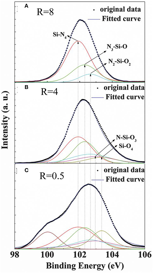
Figure 5. XPS spectra of Si 2p peaks for a-SiNxOy films with different flow rate ratios, (A) R = 8, (B) R = 4, (C) R = 0.5. The deconvolution is performed on original data denoted by the dotted line [After Dong et al. [59], with permission].
As mentioned above, any type of structure of silicon oxynitride is made up of a center Si atoms, which are tetragonally surrounded by four randomly distributed Si, N and O atoms. The following question is how to verify that the Nx-Si-Oy bonding configurations are a kind of point defect in the a-SiNxOy films?
As we know, in a-SiNx films, the structure of paramagnetic Si dangling bond (K0) defect consists of a center Si atom bonded to three N atoms and an unpaired electron (-Si=N). Habraken and Kuiper [5] derived from the EPR measurements that the g value of K0 is 2.0022 and its width ΔHpp amounts to 12.5 G. For the K0 defect family with the bonded N atoms replaced by O or Si atoms, the g value of K defect will vary from 2.0022 to 2.0055 (in which 2.0055 is the g value of pure Si dangling bond). Zhang et al. [49] reported that the g values of N-type a-SiNxOy samples with R varying from 0.5 to 8 were in the range of 2.0038–2.0026, which were located in the range of 2.0022–2.0055 (g value of K defect family) [5, 60, 61]. It means that the Nx-Si-Oy bonding configurations also acted like point defects in our N-type a-SiNxOy samples. For simplicity, in this paper we call this kind of Nx-Si-Oy bonding complex an Nx defect state. The total spin density of Nx defects was calculated to be ~1017 cm−3 by double integration of EPR signals and by correction according to a standard sample a-SiO0.8 [62]. We also confirmed that the position of the Nx defect states is located in the band gap of around 0.75 eV below the EUedge by the absorption and PL measurements.
Characteristics of Band Tail States and Defect States Dominated PL Model in a-SiOxNy
According to the typical band-tail states model proposed by Street et al. [63], Austin et al. [64] and Siebert et al. [65], the excited carriers residing in shallow tail states were thermally ionized to give rise to non-radiative decay, but those residing in deeper tail states generated luminescence via the radiative recombination. In general, the PL peak energy EPL is independent of the excitation energy Eexc when Eexc≥Eopt, while for Eexc<Eopt, the EPL will red-shift with decreasing Eexc. In our experiments [49], the phenomenon of red-shift of PL peak with decreasing Eexc can be found only in a-SiNx samples, which was shown in Figure 6B. It can be clearly seen that, when Eexc≥Eopt (3.24 eV), the EPL kept almost constant at 2.32 eV, while for Eexc<Eopt, the EPL showed a gradual red-shift down to 2.0 eV. Actually, the trace of this curve is the same as the distribution profile of band tail states. However, for the a-SiNxOy sample (R = 1.5, Eopt = 3.5 eV) EPL is independent of Eexc, regardless of whether Eexc≥Eopt or Eexc<Eopt, which was shown in Figure 6A. As for the a-SiNxOy sample with Eopt = 3.5 eV, when Eexc varied from 4.6 to 2.6 eV, EPL only changed by ~0.05 eV, which was obviously different from that of the band tail defect recombination model. We attributed this PL characteristic to the contribution from Nx defect. On the other hand, the dependence of PL integrated intensity IPL on the relative value of Eexc and Eopt in a-SiNx was also different from that in a-SiNxOy. As shown in Figure 7, under the condition of Eexc = 4.5 eV and Eexc≥Eopt, the IPL of the a-SiNx samples increases with increasing Eopt, while for a-SiNxOy samples, the IPL does not increase monotonically with Eopt, and a peak emerged at Eopt = 3.8 eV, which was probably related to the different densities of luminescent Nx defect states in the a-SiNxOy samples with various Eopt.
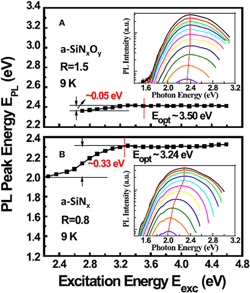
Figure 6. Characteristics of the EPL dependence on the Eexc at 9K: (A) a-SiNxOy (Eopt = 3.50 eV), (B) a-SiNx (Eopt = 3.24 eV). Inset shows PL spectra under various Eexc at 9K [After Zhang et al. [49], with permission].
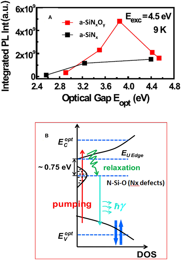
Figure 7. (A) Integrated PL intensity IPL dependence on the relative energies of Eexc and Eopt at 9K, under Eexc = 4.5 eV condition [After Zhang et al. [49], with permission]. (B) Schematic diagram of three band energy level structure in our N-type a-SiNxOy films. The N-Si-O multi-bonding defect states are located in the band gap below EUedge around 0.75 eV [After Lin et al. [69], with permission].
As shown in Figure 2B reported by Kato et al. [32], for both a-SiNx and a-SiNxOy samples, the EPL increases monotonically with increasing EUedge. This relationship is one of the characteristics of PL dominated by band tail states recombination. Herein, we plotted ΔEstokes (EUedge – EPL) vs. EUedge originated from Figure 2B, as shown in the inset of Figure 8. In Figure 8, we also found a similar relationship in our a-SiNx samples. But for the a-SiNxOy samples, ΔEstokes was independent of EUedge and was kept almost constant at around 0.75 eV below the EUedge. This phenomenon again shows the different characteristics between band tail state luminescent model and N-Si-O defect state luminescent model.
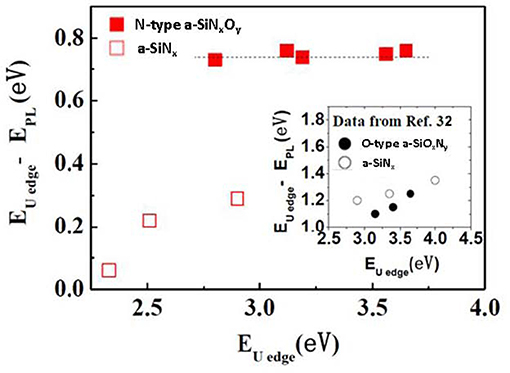
Figure 8. Correlation between the Urbach edge energy EUedge and the Stokes shift EUedge – EPL (ΔEstokes) [After Zhang et al. [49], with permission]. The data in the inset were taken from Kato et al. [32] (with permission). Closed and open symbols are for a-SiNxOy and a-SiNx, respectively.
Moreover, for analyzing the recombination processes of the photo-excited carriers, we also found the different characteristics between O-type a-SiOxNy and N-type a-SiNxOy samples. Zhang et al. [66] reported the temporal evolution trace of transient PL spectral profiles from nanosecond TRPL measurements. Figures 9A,B record the decay of TRPL intensity as a function of specific delay time at the emission wavelength of 474 nm in a-SiNxOy sample, under 8 and 300 K, respectively. The decay of TRPL intensity with specific delay time in the scale of nanosecond after excitation was shown in the Figures 9C,D, and normalized TRPL with SSPL and TIPL was shown in the Figures 9E,F. It is clearly shown that the temporal evolution of transient TRPL spectral profile did not change in both cases. The PL peak energy EPL was kept almost constant in the time scale of sub-nanoseconds to nanoseconds. This characteristic of transient PL was believed to arise from the behavior of carrier recombination through the defect states, which is obviously different from that of carrier recombination via the band-tail states, as reported by Kato et al. in Figure 3 [32].
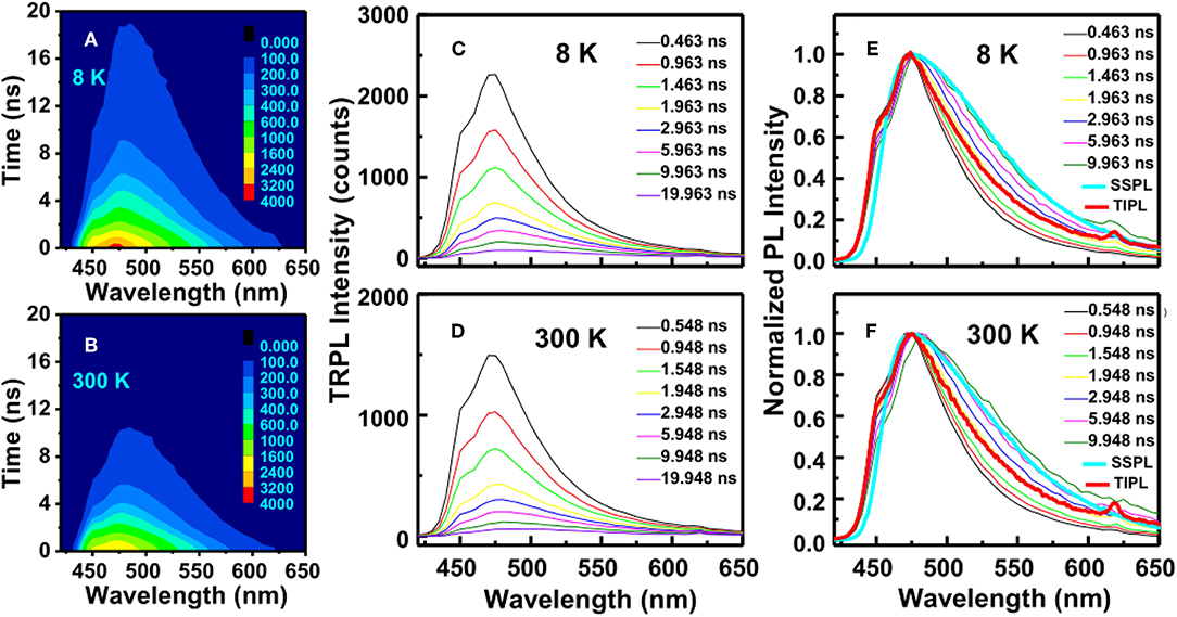
Figure 9. (A,B) TRPL intensity as a function of decay time and emission wavelength of a-SiNxOy films, under (A) 8K and (B) 300K. The color scale represents photon counts. (C,D) Temporal evolution of the transient PL at specific times after excitation, under (C) 8K and (D) 300K. (E,F) Comparison of the SSPL, TIPL, and the normalized TRPL of a-SiNxOy films, under (E) 8K and (F) 300K, respectively [After Zhang et al. [66], with permission].
Based on the differing characteristics between band tail and defect models, combined with the results of XPS, EPR with the distinct PL characteristics and absorption spectra [46], we proposed a three-level energy band system to explain the defect states recombination dominated PL model in our N-type a-SiNxOy films, which was schematically shown in Figure 7B. The N-Si-O multi-bonding defect states are located in band gap of around 0.75 eV below the EUedge. The excited electrons were quickly (~ps) relaxed down to both band tail states and Nx defect states, thereafter recombined with holes via transition between Nx defect states and valence band tail states to give rise to luminescence [49].
Improved Optical Properties in N-type a-SiNxOy Films
Despite the benefits of controlling the oxygen content in a-SiNxOy films, the optical properties of N-type a-SiNxOy films can be improved.
The PL internal quantum efficiency (PL IQE) has reached as high as 60% at the emission wavelength of 470 nm [53]. This higher PL IQE can be explained by the fast radiative recombination rate of excited carriers via the N-Si-O defect states [66]. The faster recombination rate of 108 s−1 in our a-SiNxOy films can be comparable to those with direct band gap, e.g., CdSe NCs, reported by Donega et al. [67].
Recently, Valenta et al. [68] employed Si-rich oxynitride (SRON) as well layers to fabricate SRON/SiO2 superlattice structures. After annealing at 1,150°C for 1 h, the maximum PL external quantum yield (EQY) of nearly 30% in Si nanocrystals has been observed.
Based on the three-level energy band structure, we studied the optical gain property of our N-type a-SiNxOy films. The optical gain coefficient G~102 cm−1 has been observed [69]. This kind of amplified emission can also be explained by the carrier recombination radiatively via the N-Si-O bond defect states. As mentioned above, the excited electrons go through relaxation to the N-Si-O defect states very fast (ps), while the radiative recombination lifetime is around ns, which means that the electrons remain in the N-Si-O defect states much longer than relaxation time. Consequently, population inversion of carriers between Ev and N-Si-O defect states can be realized once pumping power exceeds a threshold value.
We also investigated the performance of n-a-SiNxOy/p-Si hetero-junction (HJ) LED [30, 69]. The phosphor doped n-a-SiNxOy (ρ~2.5 Ω cm, μ~1 cm2 V−1 s−1) was deposited on the p-Si substrate to fabricate an ITO/n-a-SiNxOy/p-Si HJ LED, which was schematically shown in the inset of Figure 10A. The EL performance was shown in Figure 10B; when the bias voltage reaches ~15 V, the light emission can be observed by naked eye. For comparison, the performance of MIS LED with the structure of undoped a-SiNxOy/p-Si was shown in Figure 10C. We can see that the emission threshold voltage of 15 V for MIS LED is higher than that of n-a-SiNxOy/p-Si HJ LED. Moreover, the intensity of light output of p-n HJ LED is more than one order of magnitude higher than that of MIS LED under the same forward bias voltage, meanwhile the power efficiency of light output of p-n HJ LED is almost five times higher than that of MIS LED, which was shown in Figure 10D. The reason for the higher EL efficiency is due to the perfect balance between the electrons (n~2.4 × 1015 cm−3) in the n-a-SiNxOy layer and the holes injected from p-Si side.
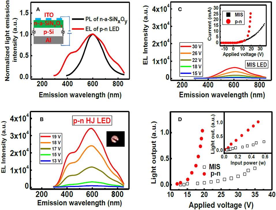
Figure 10. (A) Comparison of the PL for n-a-SiNxOy film and EL for an n-a-SiNxOy/p-Si HJ LED. The inset shows a schematic diagram of n-p HJ LED. (B) EL spectra of n-p HJ LED under different forward bias. (C) EL spectra of ITO/a-SiNxOy/p-Si MIS LED under different forward bias. The inset shows the I-V characteristics of MIS LED and p-n HJ LED. (D) The L-V characteristics of MIS LED and p-n HJ LED. The inset shows the light output as a function of the input power for two devices [After Lin et al. [69], with permission].
Finally, for the realization of all-silicon monolithically integrated optoelectronic circuits using standard CMOS processing procedures, the gate controlled Si MOSFET LED should be emphasized. Xu [70, 71] reported that, based on reversed-biased p-n junction of MOSFET operated in the avalanche breakdown mode, the gate controlled Si-LED has been demonstrated. It has been shown that the devices emit light with the wavelength in the range of 100–900 nm and could operate in the GHz range. Since, the device's operation frequency can be modified by gate signals, it can respond to both analog signal transmission and digital signal operation. Lin group reported that Si-based quantum dot (QD) [72] and Si nano-pillar array were used for enhancing the light emission quantum efficiency [73, 74].
On the other hand, direct epitaxial growth of III–V nanostructures on Si substrates is one of the most promising candidates for realizing photonic devices on a Si platform. Liu's group reported [75–77] that, at UCL, high performance InAs/GaAs QD lasers grown on Si substrates have been demonstrated in 2011 and been developing during the last 7 years.
Summary
We reviewed and discussed the present PL mechanisms in the silicon oxynitride films. Apart from preparing methods and conditions, the relative atom concentration ratio of oxygen to nitrogen (O/O+N) is a crucial factor for influencing their chemical bonding configurations and PL mechanisms. For O-type a-SiOxNy (0.6 < O/O+N < 0.9), the PL band tail and defect states recombination models have been generally agreed upon. For N-type a-SiNxOy (0.05 < O/O+N < 0.2), the N-Si-O bonding defect state recombination model has been proposed. We also analyzed the role of oxygen bonding being played in silicon oxynitride network, which not only reduced the structural disorder but also created N-Si-O (Nx) defect states in the band gap, acting as a new luminescent center. It can be found that, by modifying the chemical composition in these non-stoichiometric silicon oxynitride materials, the optical and electronic properties can be improved. Finally, the n-a-SiNxOy/p-Si HJ LED fabricated by the standard CMOS technology has been also demonstrated.
Author Contributions
KC is an advisor and wrote this manuscript. ZL, PZ, and HD carried out experiments and analyzed experimental results. RH did the initial work. XH gave some suggestion and comments on this work.
Funding
The work was supported by National Nature Science Foundation of China Grant No. 11374153 and National Key R&D Program of China Grant No. 2018YFB2200101, and the Scientific Research Program of 333 Project of Jiangsu Province Grant No. BRA2019188.
Conflict of Interest
The authors declare that the research was conducted in the absence of any commercial or financial relationships that could be construed as a potential conflict of interest.
References
1. Fukuda H, Arakawa T, Ohno S. Highly reliable thin nitrided SiO2 film formed by rapid thermal processing in an N2O ambient. Electron Lett. (1990) 26:1505–6. doi: 10.7567/SSDM.1990.C-2-1
2. Hwang H, Ting W, Maiti B, Kwong DL, Lee J. Effects of reoxidation on band alignment in N-incorporated SiON films as a function of sequential thermal annealing in NO and NH3. Appl Phys Lett. (1990) 57:1010–1.
3. Gusev EP, Lu HC, Gustafsson T, Garfunkel E, Green ML, Brasen D. The composition of ultrathin silicon oxynitrides thermally grown in nitric oxide. J Appl Phys. (1997) 82:896–8. doi: 10.1063/1.365858
4. Lucovsky G. Monolayer incorporation of nitrogen at Si–SiO2 interfaces: interface characterization and electrical properties. J Vac Sci Technol A. (1998) 16:356–64. doi: 10.1116/1.581005
5. Habraken FHPM, Kuiper AET. Silicon nitride and oxynitride films. Mater Sci Eng R. (1994) 12:123–75. doi: 10.1016/0927-796X(94)90006-X
6. Daldosso N, Luppi M, Ossicini S, Degoli E, Magri R, Dalba G, et al. Role of the interface region on the optoelectronic properties of silicon nanocrystals embedded in SiO2. Phys Rev B. (2003) 68:085327. doi: 10.1103/PhysRevB.68.085327
7. Hussey KL, Hoffman TL, Tao Y, Graham MJ. A study of nitrogen incorporation during the oxidation of Si(100) in N2O at high temperatures. J Electrochem Soc. (1996) 143:221–8. doi: 10.1149/1.1836412
8. Matsuoka T, Kakimoto S, Nakano M, Kotaki H, Hayashida S, Sugimoto K, et al. Direct tunneling N2O gate oxynitrides for low-voltage operation of dual gate CMOSFETs. In: Technical Digest - International Electron Devices Meeting. Washington, DC (1995). p. 851–54.
9. Carr EC, Ellis KA, Buhrman RA. N depth profiles in thin SiO2 grown or processed in N2O: the role of atomic oxygen. Appl Phys Lett. (1995) 66:1492–4. doi: 10.1063/1.113665
10. Bouvet D, Clivaz PA, Dutoit M, Coluzza C, Almeida J, Margaritondo G, et al. Influence of nitrogen profile on electrical characteristics of furnace- or rapid thermally nitrided silicon dioxide films. J Appl Phys. (1996) 79:7114–22. doi: 10.1063/1.361481
11. Yao ZQ. The nature and distribution of nitrogen in silicon oxynitride grown on silicon in a nitric oxide ambient. J Appl Phys. (1995) 78:2906–12. doi: 10.1063/1.360036
12. Hegde RI, Tobin PJ, Reid KG, Maiti B, Ajuria SA. Growth and surface chemistry of oxynitride gate dielectric using nitric oxide. Appl Phys Lett. (1995) 66:2882–4. doi: 10.1063/1.113461
13. Takami S, Egashira Y, Honma I, Komiyama H. Monolayer nitridation of silicon surfaces by a dry chemical process using dimethylhydrazine or ammonia. Appl Phys Lett. (1995) 66:1527–9. doi: 10.1063/1.113635
14. Yount JT, Lenahan PM, Krick JT. Comparison of defect structure in N2O- and NH3-nitrided oxide dielectrics. J Appl Phys. (1994) 76:1754–8. doi: 10.1063/1.357692
15. Bhat M, Ahn J, Kwong DL, Arendt M, White JM. Comparison of the chemical structure and composition between N2O oxides and reoxidized NH3-nitrided oxides. Appl Phys Lett. (1994) 64:1168–70. doi: 10.1063/1.111951
16. Bellafiore N, Pio F, Riva C. Thin SiO2 films nitrided in N2O. Microelectron J. (1994) 25:495–500. doi: 10.1016/0026-2692(94)90033-7
17. Ito T, Kitayama D, Ikoma H. Silicon oxynitridation with inductively coupled oxygen–nitrogen mixed plasma. Jpn J Appl Phys. (1997) 36:612–6. doi: 10.1143/JJAP.36.612
18. Masuda A, Yonezawa Y, Morimoto A, Kumeda M, Shimizu T. Ultrathin SiO2 films on Si formed by N2O-plasma oxidation technique. Appl Surf Sci. (1994) 81:277–80. doi: 10.1016/0169-4332(94)90284-4
19. Kaluri SR, Hess DW. Nitrogen incorporation in thin oxides by constant current N2O plasma anodization of silicon and N2 plasma nitridation of silicon oxides. Appl Phys Lett. (1996) 69:1053–5. doi: 10.1063/1.116928
20. Gusev EP, Lu HC, Garfunkel E, Gustafsson T, Green M. Growth and characterization of ultrathin nitrided silicon oxide films. IBM J Res Dev. (1999) 43:265–86. doi: 10.1147/rd.433.0265
21. Chang JP, Green ML, Donnelly VM, Opila RL, Eng J Jr, Sapjeta J, et al. Profiling nitrogen in ultrathin silicon oxynitrides with angle-resolved x-ray photoelectron spectroscopy. J Appl Phys. (2000) 87:4449–55. doi: 10.1063/1.373090
22. Green ML, Gusev EP, Degraeve R, Garfunkel EL. Ultrathin (<4 nm) SiO2 and Si–O–N gate dielectric layers for silicon microelectronics: understanding the processing, structure, and physical and electrical limits. J Appl Phys. (2001) 90:2057–121. doi: 10.1063/1.1385803
23. Mogensen KB, Friis P, Hubner J, Petersen NJ, Jorgensen AM, Telleman P, et al. Ultraviolet transparent silicon oxynitride waveguides for biochemical microsystems. Opt Lett. (2001) 26:716–8. doi: 10.1364/OL.26.000716
24. Kato H, Fujimaki M, Noma T, Ohki Y. Photo-induced refractive index change in hydrogenated amorphous silicon oxynitride. J Appl Phys. (2002) 91:6350–3. doi: 10.1063/1.1461894
25. Gorin A, Jaouad A, Grondin E, Aimez V, Charette P. Fabrication of silicon nitride waveguides for visible-light using PECVD: a study of the effect of plasma frequency on optical properties. Opt Exp. (2008) 16:13509–16. doi: 10.1364/OE.16.013509
26. Rebohle L, Gebel T, Yankov RA, Trautmann T, Skorupa W, Sun JM, et al. Microarrays of silicon-based light emitters for novel biosensor and lab-on-a-chip applications. Opt Mater. (2005) 27:1055–8. doi: 10.1016/j.optmat.2004.08.062
27. Patil U, Fihri A, Emwas AH, Polshettiwar V. Silicon oxynitride of KCC-1, SBA-15, and MCM-41 for CO2 capture with excellent stability and regenerability. Chem Sci. (2012) 3:2224–9. doi: 10.1039/c2sc20356a
28. Modreanu M, Gartner M, Cristea D. Investigation on preparation and physical properties of LPCVD SixOyNz thin films and nanocrystalline Si/SixOyNz superlattices for Si-based light emitting devices. Mater Sci Eng C. (2002) 19:225–8. doi: 10.1016/S0928-4931(01)00471-4
29. Huang R, Chen K, Han P, Dong H, Wang X, Chen D, et al. Strong green-yellow electroluminescence from oxidized amorphous silicon nitride light-emitting devices. Appl Phys Lett. (2007) 90:093515. doi: 10.1063/1.2711196
30. Lin Z, Chen K, Zhang P, Xu J, Li W, Yang H, et al. Improved power efficiency in phosphorus doped n-a-SiNxOy/p-Si heterojunction light emitting diode. Appl Phys Lett. (2017) 110:081109. doi: 10.1063/1.4977419
31. Kerr MJ, Schmidt J, Cuevas A, Bultman JH. Surface recombination velocity of phosphorus-diffused silicon solar cell emitters passivated with plasma enhanced chemical vapor deposited silicon nitride and thermal silicon oxide. J Appl Phys. (2001) 89:3821–6. doi: 10.1063/1.1350633
32. Kato H, Kashio N, Ohki Y, Seol KS, Noma T. Band-tail photoluminescence in hydrogenated amorphous silicon oxynitride and silicon nitride films. J Appl Phys. (2003) 93:239–44. doi: 10.1063/1.1529292
33. Noma T, Seol KS, Kato H, Fujimaki M. Origin of photoluminescence around 2.6–2.9 eV in silicon oxynitride. Appl Phys Lett. (2001) 79:1995–7. doi: 10.1063/1.1405806
34. Price KJ, McNeil LE, Suvkanov A, Irene EA, MacFarlane PJ, Zvanut ME. Characterization of the luminescence center in photo- and electroluminescent amorphous silicon oxynitride films. J Appl Phys. (1999) 86:2628–37. doi: 10.1063/1.371102
35. Augustine BH, Hu YZ, Irene EA, McNeil LE. An annealing study of luminescent amorphous silicon-rich silicon oxynitride thin films. Appl Phys Lett. (1995) 67:3694–6. doi: 10.1063/1.115352
36. Augustine BH, Irene EA, He YJ, Price KJ, McNeil LE, Christensen KN, et al. Visible light emission from thin films containing Si, O, N, and H. J Appl Phys. (1995) 78:4020–30. doi: 10.1063/1.359925
37. Price KJ, Sharpe LR, McNeil LE, Irene EA. Electroluminescence in silicon oxynitride films. J Appl Phys. (1999) 86:2638–41. doi: 10.1063/1.371103
38. Deshpande SV, Gulari E, Brown SW, Rand SC. Optical properties of silicon nitride films deposited by hot filament chemical vapor deposition. J Appl Phys. (1995) 77:6534–41. doi: 10.1063/1.359062
39. Kenyon AJ, Trwoga PF, Pitt CW, Rehm G. The origin of photoluminescence from thin films of silicon-rich silica. J Appl Phys. (1996) 79:9291–300. doi: 10.1063/1.362605
40. Noma T, Seol KS, Fujimaki M, Kato H, Watanabe T, Ohki Y. Photoluminescence analysis of plasma-deposited oxygen-rich silicon oxynitride films. Jpn J Appl Phys. (2000) 39(Pt 1):6587–93. doi: 10.1143/JJAP.39.6587
41. Kato H, Masuzawa A, Noma T, Seol KS, Ohki Y. Thermally induced photoluminescence quenching centre in hydrogenated amorphous silicon oxynitride. J Phys. (2001) 13:6541–9. doi: 10.1088/0953-8984/13/30/310
42. Kato H, Masuzawa A, Sato H, Noma T, Seol KS, Fujimaki M, et al. Visible electroluminescence in hydrogenated amorphous silicon oxynitride. J Appl Phys. (2001) 90:2216–20. doi: 10.1063/1.1388864
43. Tewary A, Kekatpure RD, Brongersma ML. Controlling defect and Si nanoparticle luminescence from silicon oxynitride films with CO2 laser annealing. Appl Phys Lett. (2006) 88:093114. doi: 10.1063/1.2178769
44. Huang R, Chen K, Qian B, Chen S, Li W, Xu J, et al. Oxygen induced strong green light emission from low-temperature grown amorphous silicon nitride films. Appl Phys Lett. (2006) 89:221120–3. doi: 10.1063/1.2399393
45. Huang R, Chen K, Dong H, Wang D, Ding H, Li W, et al. Enhanced electroluminescence efficiency of oxidized amorphous silicon nitride light-emitting devices by modulating ratio. Appl Phys Lett. (2007) 91:111104. doi: 10.1063/1.2783271
46. Dong H, Chen K, Wang D, Li W, Ma Z, Xu J, et al. A new luminescent defect state in low temperature grown amorphous SiNxOy thin films. Phys Status Solidi C. (2010) 7:828–31. doi: 10.1002/pssc.200982770
47. Ruggeri R, Neri F, Sciuto A, Privitera V, Spinella C, Mannino G. Luminescence properties of SiOxNy irradiated by IR laser 808 nm: the role of Si quantum dots and Si chemical environment. Appl Phys Lett. (2012) 100:042104. doi: 10.1063/1.3679395
48. Jou S, Liaw I-C, Cheng Y-C, Li C-H. Light emission of silicon oxynitride films prepared by reactive sputtering of silicon. J Lumin. (2013) 134:853–7. doi: 10.1016/j.jlumin.2012.06.037
49. Zhang P, Chen K, Lin Z, Dong H, Li W, Xu J, et al. The role of N-Si-O bonding configurations in tunable photoluminescence of oxygenated amorphous silicon nitride films. Appl Phys Lett. (2015) 106:231103. doi: 10.1063/1.4922465
50. Wolkin MV, Jorne J, Fauchet PM, Allan G, Delerue C. Electronic states and luminescence in porous silicon quantum dots: the role of oxygen. Phys Rev Lett. (1999) 82:197–200. doi: 10.1103/PhysRevLett.82.197
51. Pavesi L, Negro LD, Mazzoleni C, Franzo G, Priolo F. Optical gain in silicon nanocrystals. Nature. (2000) 408:440–4. doi: 10.1038/35044012
52. Denisse CMM, Troost KZ, Habraken FHPM, Weg WF, Hendriks M. Annealing of plasma silicon oxynitride films. J Appl Phys. (1986) 60:2543–7. doi: 10.1063/1.337118
53. Zhang P, Chen K, Dong H, Zhang P, Fang Z, Li W, et al. Higher than 60% internal quantum efficiency of photoluminescence from amorphous silicon oxynitride thin films at wavelength of 470 nm. Appl Phys Lett. (2014) 105:011113. doi: 10.1063/1.4887058
54. Wong H, Gritsenko VA. Defects in silicon oxynitride gate dielectric films. Microelectron Reliab. (2002) 42:597–605. doi: 10.1016/S0026-2714(02)00005-7
55. Cova P, Poulin S, Grenier O, Masut RA. A method for the analysis of multiphase bonding structures in amorphous films. J Appl Phys. (2005) 97:073518. doi: 10.1063/1.1881774
56. Naskar S, Wolter SD, Bower CA, Stoner BR, Glass JT. Verification of the O–Si–N complex in plasma-enhanced chemical vapor deposition silicon oxynitride films. Appl Phys Lett. (2005) 87:261907. doi: 10.1063/1.2158022
57. Ding W, Li L, Zhang L, Ju D, Peng S, Chai W. An XPS study on the chemical bond structure at the interface between SiOxNy and N doped polyethylene terephthalate. J Chem Phys. (2013) 138:104706. doi: 10.1063/1.4794782
58. Nguyen PD, Kepaptsoglou DM, Ramasse QM, Sunding MF, Vestland LO, Finstad TG, et al. Impact of oxygen bonding on the atomic structure and photoluminescence properties of Si-rich silicon nitride thin films. J Appl Phys. (2012) 112:073514. doi: 10.1063/1.4756998
59. Dong H, Chen K, Zhang P, Li W, Xu J, Ma Z, et al. The role of Nx-Si–Oy bonding configuration in acquiring strong blue to red photoluminescence from amorphous SiNxOy film. Can J Phys. (2014) 92:602–5. doi: 10.1139/cjp-2013-0609
60. Cros Y, Krautwurm J. Structural identification of point defects in amorphous silicon oxynitrides. J Noncryst Solids. (1995) 187:385–94. doi: 10.1016/0022-3093(95)00169-7
61. Warren WL, Kanicki J, Poindexter EH. Paramagnetic point defects in silicon nitride and silicon oxynitride thin films on silicon. Colloids Surf. (1996) 115:311–7. doi: 10.1016/0927-7757(96)03595-9
62. Wang YF, Chen KJ, Qian XY, Fang ZF, Li W, Xu J. The x dependent two kinds of resistive switching behaviors in SiOx films with different x component. Appl Phys Lett. (2014) 104:012112. doi: 10.1063/1.4861592
63. Street RA. Luminescence and recombination in hydrogenated amorphous silicon. Adv Phys. (1981) 30:593–676. doi: 10.1080/00018738100101417
64. Austin IG, Jackson WA, Searle TM, Bhat PK, Gibson RA. Photoluminescence properties of a-SiNx: H alloys. Philos Mag B. (1985) 52:271–88. doi: 10.1080/13642818508240600
65. Siebert W, Carius R, Fuhs W, Jahn K. Photoluminescence in a-Si1−−xCx:H films. Phys Status Solidi B. (1987) 140:311–21. doi: 10.1002/pssb.2221400132
66. Zhang P, Chen K, Lin Z, Tan D, Dong H, Li W, et al. Dynamics of high quantum efficiency photoluminescence from N-Si-O bonding states in oxygenated amorphous silicon nitride films. Appl Phys Lett. (2016) 108:111103. doi: 10.1063/1.4944056
67. Donega CM, Hickey SG, Wuister SF, Vanmaekelbergh D, Meijerink A. Single-step synthesis to control the photoluminescence quantum yield and size dispersion of CdSe nanocrystals. J Phys Chem B. (2003) 107:489–96. doi: 10.1021/jp027160c
68. Valenta J, Greben M, Gutsch S, Hiller D, Zacharias M. Photoluminescence performance limits of Si nanocrystals in silicon oxynitride matrices. J Appl Phys. (2017) 122:144303–9. doi: 10.1063/1.4999023
69. Lin Z, Chen K, Zhang P, Xu J, Dong H, Li W, et al. The role of N-Si-O defect states in optical gain from an a-SiNxOy/SiO2 waveguide and in light emission from an n-a-SiNxOy/p-Si heterojunction LED. Phys Status Solidi A. (2018) 215:1700750. doi: 10.1002/pssa.201700750
70. Xu K. Integrated silicon directly modulated light source using p-well in standard CMOS technology. IEEE Sensors J. (2016) 16:6184–91. doi: 10.1109/JSEN.2016.2582840
71. Xu K. Silicon MOS optoelectronic micro-nano structure based on reverse biased PN junction. Phys Status Solidi A Syst. (2019) 216:1800868–9. doi: 10.1002/pssa.201800868
72. Lin CJ, Lin GR. Defect-enhanced visible electroluminescence of multi-energy silicon-implanted silicon dioxide film. IEEE J Quantum Electron. (2005) 41:441–7. doi: 10.1109/JQE.2004.842314
73. Lin GR, Pai YH, Lin CT. Microwatt MOSLED using SiOx with buried Si nanocrystals on Si nano-pillar array. J Lightwave Technol. (2008) 26:1486–91. doi: 10.1109/JLT.2008.922177
74. Cheng CH, Lien YC, Wu CL, Lin GR. Multicolor electroluminescent Si quantum dots embedded in SiOx thin film MOSLED with 2.4% external quantum efficiency. Opt Express. (2013) 21:391–403. doi: 10.1364/OE.21.000391
75. Liu H, Wang T, Jiang Q, Hogg R, Tutu F, Pozzi F, et al. Long-wavelength InAs/GaAs quantum-dot laser diode monolithically grown on Ge substrate. Nat Photonics. (2011) 5:416–9. doi: 10.1038/nphoton.2011.120
76. Tang M, Chen S, Wu J, Jiang Q, Kennedy K, Jurczak P, et al. Optimizations of defect filter layers for 1.3-um InAs/GaAs quantum-dot lasers monolithically grown on Si substrates. IEEE J Sel Top Quantum Electron. (2016) 22:1900207–8. doi: 10.1109/JSTQE.2016.2551941
Keywords: amorphous silicon oxynitride (a-SiNxOy), PL mechanism, band tail model, N-Si-O bond defect model, a-SiNxOy LED
Citation: Chen K, Lin Z, Zhang P, Huang R, Dong H and Huang X (2019) Luminescence Mechanism in Amorphous Silicon Oxynitride Films: Band Tail Model or N-Si-O Bond Defects Model. Front. Phys. 7:144. doi: 10.3389/fphy.2019.00144
Received: 01 May 2019; Accepted: 13 September 2019;
Published: 02 October 2019.
Edited by:
Simona Binetti, University of Milano Bicocca, ItalyReviewed by:
Kaikai Xu, University of Electronic Science and Technology of China, ChinaDongsheng Li, Zhejiang University, China
Copyright © 2019 Chen, Lin, Zhang, Huang, Dong and Huang. This is an open-access article distributed under the terms of the Creative Commons Attribution License (CC BY). The use, distribution or reproduction in other forums is permitted, provided the original author(s) and the copyright owner(s) are credited and that the original publication in this journal is cited, in accordance with accepted academic practice. No use, distribution or reproduction is permitted which does not comply with these terms.
*Correspondence: Kunji Chen, a2pjaGVuQG5qdS5lZHUuY24=