 Jacopo Parravicini1
 Francesco Arcadi1†
 Alessia Le Donne1Roberta Campesato2Mariacristina Casale2Erminio Greco2
 Simona Binetti1*
- 1Dipartimento di Scienza dei Materiali, MIBSOLAR Center, Università di Milano-Bicocca, Milan, Italy
- 2CESI s.p.a., Milan, Italy
The most common multi-junction solar cell arrangement employs the InGaP/InGaAs/Ge configuration, which is usually exploited for high-efficiency space applications. We here test the reliability of a triple-junction device with an innovative low-thickness and flexible configuration: this is investigation is aimed at providing its main macroscopic features which must be taken into account for their applications. Notably, the specific optical and electrical features and the performance variation of these thin solar cells are systematically analyzed, both in begin-of-life (BOL) configuration and after irradiation (end-of-life, EOL) by either electrons or protons. Measurements of I – V curves, with correlated parameters, and of spectral responses (external quantum efficiency) are accomplished on several BOL and EOL samples: this allows to describe the inhomogeneous damage of the subjunctions and to follow the evolution of the solar cell physical quantities as a function of the kind and the amount of irradiation. Finally, photoluminescence emission spectra are measured, pointing out the effect of particle bombardment on luminescent features. Our results show that these innovative solar devices allow for the combination of high specific power, mechanical flexibility, high performance, and strong resistance to particle irradiation, making them an excellent option for space applications.
Introduction
Multi-junction III–V solar cells are widely employed in space applications, due to their high efficiency outside the terrestrial atmosphere. The most employed configuration exploits InGaP/InGaAs/Ge-based devices, reaching well-established performance and reliability [1–3]. These very high efficiency solar devices based on III–V compounds are still the best approach to increase the specific and the solar arrays lifetime. Actually, some key features are mandatory in such equipments: the first one is radiation resistance, due to the fact that during their operative life a strong bombardment of charged electrons and protons is present [4–12]; the second issue is the need of low-weight devices with high specific power [3]. In addition to these, a further request recently has arisen of increasing versatility and adaptability to the spacecrafts by having bendable and mechanically flexible solar arrays [13–17]. These issues suggest that new designs of multi-junction high-efficiency solar cells must be devised: a fruitful approach is based on manufacturing multi-junction III-V solar cells with thin substrates (typically <100 μm), which should allow both lightness (high specific power) and structural flexibility [18, 19]. Such technologies have the potential to strongly decrease the mass of the photovoltaic device, with beneficial effects also on the cost of the solar cells. A specific class of thin multi-junction solar devices fulfilling these requested features is the CTJ30-80 technology, which has been developed and qualified according to the European Spatial Agency (ESA) specific protocols by Centro Elettrotecnico Sperimentale Italiano (CESI) [20].
In this work we systematically investigate the performance evolution of such kind of devices as a function of particle irradiation. Specifically, thin multi-junction cells (with thickness ≃80 μm) have been irradiated both by electrons and protons, in order to reproduce the operative condition of such space devices. Several physical quantities are analyzed to describe the macroscopic features of the devices, with the specific aim of providing their response and reliability during practical uses. Notably, we test the electrical behavior before (begin-of-life conditions, BOL) and after (end-of-life conditions, EOL) irradiation of electrons and protons: the obtained performance is discussed and correlated with the particle bombardment to reproduce the real working conditions of the devices. In particular, the comparison of the electric features with the external quantum efficiency (EQE) as a function of the exciting wavelength (spectral response measurements) provides a fine description of each subcell behavior. Finally, photoluminescence spectra measurements on top and middle subcells are carried out and discussed in order to obtain information about the irradiation-induced radiative point defects.
Materials and Methods
Sample Features
The studied samples are CTJ30-80 solar devices manufactured by CESI: they are InGaP/InGaAs/Ge triple junction solar cells with a size of 26.5 cm2 and AM0 efficiency class 30%, which have been manufactured and qualified in accordance with the standard ESA ECSS E ST20-08C Rev. 1 [19]. Such devices are based on the CTJ30 CESI technology, a class of solar cells with standard thickness of 140 μm which are used on several satellites since 2013 [21]. In CTJ30 devices, the conversion efficiency is increased by adding Bragg reflectors inside the solar cell stack (Figure 1A) and by a fine tuning of the electrical field inside the solar cell active regions [18]. Specific previous studies on irradiated thick CTJ30 solar cells demonstrated that the introduction of this Bragg structure is able to increase the performance of the solar cell both in BOL and EOL conditions. The irradiation damage were evaluated by calculating the remaining factors, a figure of merit specifically employed in these kind of studies [22]. Indeed, the qualification campaign highlighted very good resistance under electron and proton irradiation [23]. CTJ30-80 cells are suitably thinned until 80 μm to decrease the mass of the solar cells and to obtain mechanically flexible devices. Such thin space solar cells have been developed and grown up with an InGaP/InGaAs/Ge epitaxial structure: growth procedure is carried out through the Veeco E450G MOCVD industrial reactor equipped with carriers in order to simultaneously hold up to 13 Ge substrates per run. The multi-layers structures are grown on 100-mm diameter and 140 μm-thick Ge substrates. After the epitaxial growth the Ge substrate has been thinned down to 80 μm using a suitable wet etch process, whose details are protected by trade secret. We note that such a thinning process could modify the features of both the interfaces and the active layers. Namely, it can cause either the diffusion of impurities or the arising of microcracking due to a mechanical weakening of the overall structure. A systematic investigation of the cell performance is therefore mandatory to guarantee a suitable reliability for the usual applications on spacecrafts. From each wafer two solar devices, with 26.5 cm2 size and typical 1.3 g mass, are obtained. The front and rear contacts are made by evaporated silver 5 μm-thick, capped with 200 nm gold. The broadband AR coating is an optimized dual-layers Ta2O5/SiO2.
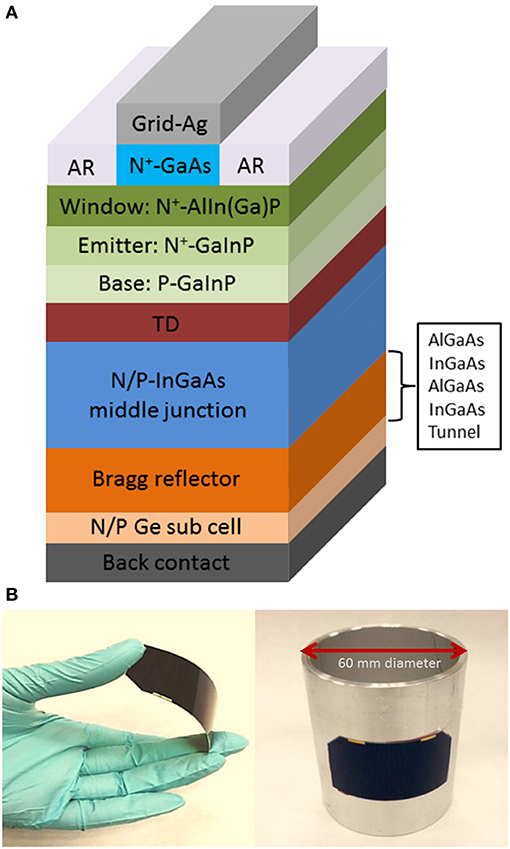
Figure 1. (A) Scheme of the structure of CTJ30-80 solar cell. Each subjunction has a thickness of few μm and (B) pictures of a CTJ30-80 solar cell in a demonstrative bent configurations, highlighting its specific mechanical flexibility.
Experimental Setup
The electrical performance is measured in comparison with Secondary Working Standard sets that have been calibrated by INTA-Spasolab. A batch of 50 cells has been selected at random for the qualification campaign at bare solar cell level. The selected conditions allow to obtain thin substrates with good thickness uniformity, without significant degradation of the electrical performances with respect to the standard 140 μm-thick (CESI CTJ30) solar cells [20, 23]: despite their smaller thickness, a 29% efficiency AM0, 25°C has been demonstrated on these devices, together with a bending radius of 30 mm [19] (see Figure 1B). As the etch-based thinning process is carried out on the substrate only, the decrease of the device thickness is obtained without influencing the subcell layers. This makes possible to decrease the weight nearly 50% of the whole device without marked loosing of power: actually CTJ30-80 cells reach a specific power of about 1 W/g, roughly doubled with respect to the standard CTJ30 structure (0.5 W/g). This opens the way for a fruitfully future application on light and flexible solar arrays.
Two sets of 25 cells from the batch have been prepared, for electron and proton irradiation respectively. Following the ECSS E-ST-20-0 test procedure, all cells to be validated are subjected to suitable thermal and photon annealing: they are kept at 60°C for 24 h under AM0 illumination. The samples have an area of 26.5 cm2 and were electron-irradiated with intensities from 1 × 10¹⁴ to 3 × 10¹⁵ e−/cm2 at Technical University of Delft (The Nederlands) and proton-irradiated with intensities from 1 × 10¹⁰ to 1.5 × 10¹¹ p+/cm2 at Paris CNRSM (France), both with Van Der Graaf accelerators. In both cases the employed energies were 1 MeV.
For I–V measurement we have used a solar simulator WACOM WXS130S, equipped with a Xe-lamp and suitable filters, providing an AM0 spectrum. This has been controlled with specific reference cells at each measurement. I–V curves are acquired through suitable interfaces and softwares: the software is a customized version SoCRATeS system provided by the company IPSES s.r.l. Before each measurement session a calibration phase is accomplished by using a set of three Secondary Working Standard (SWS) single-junction calibration cells, an InGaP-based, reproducing the top-subcell (Top calibration cell), an InGaAs-based, reproducing the middle subcell (Middle calibration cell), and a Ge-based, reproducing the bottom subcell (Bottom calibration cell) of the CTJ30-80. The light intensity is measured to be constant on the whole surface of the sample holder within 1%.
A fruitful and synthetic evaluation of the irradiated cell degradation can be obtained by defining the specific figures of merit of remaining factors R [22]. Each remaining factor R can be defined in correspondence with Voc, Isc, Pmax, FF, η. RV is defined by
where VBOL is the Voc value of the begin-of-life cell and VEOL is the Voc value of the cell after irradiation (end-of-life). Analogously to (1) we define RI, RP, RFF, Rη in correlation with Isc, Pmax, FF, η of BOL and EOL cells respectively, i.e.,
Such I–V measurements provide an overall picture of the device response to the irradiation. A more detailed investigation of each junction behavior can be carried out by using the wavelength-resolved external-quantum-efficiency (EQE) measurement for tandem and multi-junction solar cells with a light-bias method: this is a well-established and diffused technique which evaluates the efficiency of internal current generation in respective subcells as a function of each different illuminating wavelengths [24–27]. In this study, the response of each subjunction of each solar device has been tested through EQE measurements by exploiting the standard commercial apparatus SpeQuest of ReRa Solutions for spectral response measurements.
For photoluminescence (PL) measurements we have employed two experimental setups. All PL measurements in the 900–1'700 nm range are performed with a spectral resolution of 6.6 nm with an excitation wavelength of λexc = 805 nm provided by a laser source. Detection is accomplished with a standard lock-in technique in conjunction with a single grating monochromator and an InGaAs detector. For the 250–800 nm range the employed light source is a Xe lamp of 450 W with an emission peak at 467 nm. The monochromator of the excitation stage employs two gratings. The detection stage uses a Hamamatsu R928P phototube with a sensitivity in the 195–900 nm region and a maximum response at 400 nm.
Results: Electric and Optical Features
Electron Irradiation
We test a bunch of 25 CTJ30-80 electron-irradiated thin cells. Five sets of 5 cells have been prepared: each set is irradiated with a given dose of radiations, i.e., 5 × 10¹³, 1 × 10¹⁴, 5 × 10¹⁴, 1 × 10¹⁵, and 3 × 10¹⁵ e−/cm2. The energy of the electrons is fixed at 1 MeV. 2 cells of each 5 cell set are used for the here considered irradiation tests, while 3 of them are subjected to different feasibility tests (contact adherence, extended storage simulation, etc.), which are not reported nor discussed here. Three measurements are accomplished on each irradiated sample, whose values are averaged; for each irradiation dose, the reported measurement is the average of the response of 2 samples. The electron irradiation tests on standard 140-μm-thick CTJ30 cells, whose results are reported in Campesato et al. [23], were performed with the same doses here considered. Results showed that the middle subcell progressively deteriorates as the dose increases, while the top cell is almost unaffected; the top subcell, however, still remains the current-limiting one even at the highest dose [23].
The overall performance of the irradiated CTJ30-80 devices is inspected through standard I–V measurements, while the responses of each active component are investigated by spectral EQE experiments. We note that the analysis of the remaining factors provides a global information, which points out the response of the whole multi-junction cell, while the behavior of each single junction can be distinguished by considering their respective EOL spectral responses, i.e., EQE responses, and comparing them to BOL behavior. This allows to finely analyze the subcell degradation. The correlated curves are depicted in Figures 2A,B. The obtained electric parameters and spectral response are measured on two samples for each irradiation dose, so 10 samples are measured.
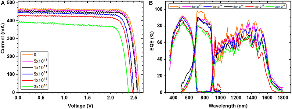
Figure 2. (A) I–V curves and (B) spectral responses of the thin cells in BOL and EOL configurations. The doses are given in e−/cm2 units. Note that the experimental noise grows from top to bottom junction.
The averaged electric responses of the BOL and EOL cells are reported in Table 1.
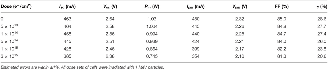
Table 1. Averaged electric performance (at 25°C) of the BOL and electron-irradiated EOL cells.
In these tables Isc and Voc are respectively the short-circuit current and the open-circuit voltage, Pm is the maximum power supplied by the cell, Ipm and Vpm are the amounts of current and voltage in correspondence with the maximum power, FF is the Fill-Factor and η is the efficiency. The estimated relative error of both the reported currents and voltages is within 1%, causing and error of about 0.5 and 1% on the FF and efficiency estimation respectively.
It is worth following the evolution of the electric parameters as a function of the electron irradiation dose by the correlated remaining factors. They are depicted in Figure 3 and summarized in Table 2.
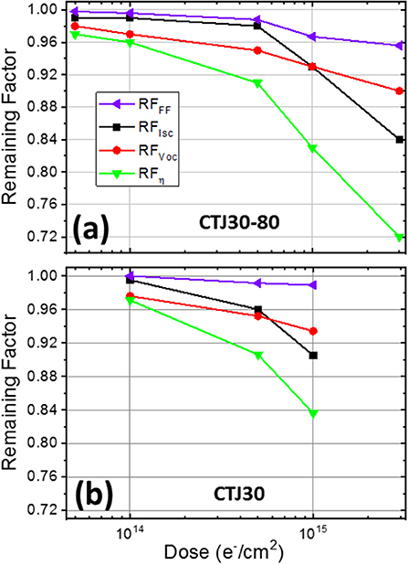
Figure 3. Remaining factors of Isc, Voc, FF, η as a function of the electron irradiation dose: comparison between the trend of (a) the here discussed (thin) CTJ30-80 devices and (b) the (thick) CTJ30 devices.
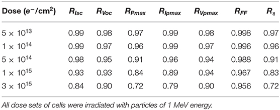
Table 2. Remaining factors of the electric performance of electron-irradiated cells for each particle dose.
The plot Figure 3a shows that the η parameter undergoes the greatest degradation, which is strongly influenced by the decrease of Isc and Voc. In particular, it is evident that RI remains near 1 (unchanged current) for the first doses and drops down suddenly when irradiation overcomes 5 × 10¹⁴ e−/cm2. More specifically, we associate the trends in Figure 3a mainly to the change of the current-limiting junction. Namely, for low irradiation doses the overall solar cell still remains in a configuration where the InGaP top subcell limits the device current. Conversely, when the irradiation dose overcomes the threshold of about 5 × 10¹⁴ e−/cm2 the degradation of the middle subcell makes it the limiting junction, causing a marked decrease of the remaining factors.
The behavior of these remaining factors (Figure 3a) is compared with that of the standard thick CTJ30 cells in Figure 3b. First we note that the global behavior of the remaining factors in these two plots is very similar, pointing out a response of the considered thin cells to the electron irradiation which is fully analogous to that of the thick standard cells.
The EQE spectra of the subcells are depicted in Figure 2B, providing the response of each subjunction to each wavelength; the product of this one by the spectrum of the employed AM0 solar simulator is integrated to obtain short-circuit currents Isc [2]. The ratios between the calculated short-circuit currents of BOL and EOL subcells are reported in Table 3. It should be noted that the evaluation of electric parameters from EQE measurements can be affected by relatively high errors [28]: in our case we estimate ≃ ±3% for the top subcells, ≃ ±7% for the middle subcells, and ≃ ±10–13% for the bottom subcells. However, we can assume the ratios in Table 3 as a qualitative figure of merit of the subcell degradations.
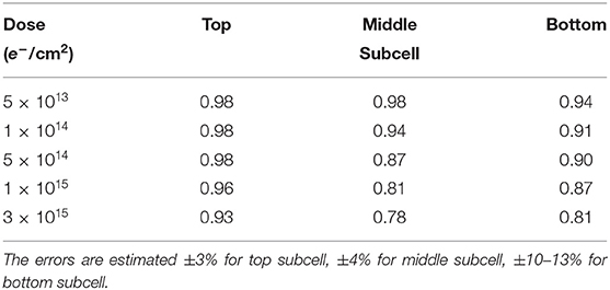
Table 3. Ratios between short-circuit currents of BOL and EOL subcells calculated by EQE measurements for different electron irradiations.
The plot in Figure 4 reports the ratio between the currents, calculated from the spectral measurements, of the top and middle subcells as a function of the irradiation dose. Actually this ratio becomes larger than 1 over the dose of 5 × 10¹⁴ e−/cm2, pointing out that after this dose the limiting subcell becomes the middle one: this confirms the change of the limiting subcell above this threshold dose.
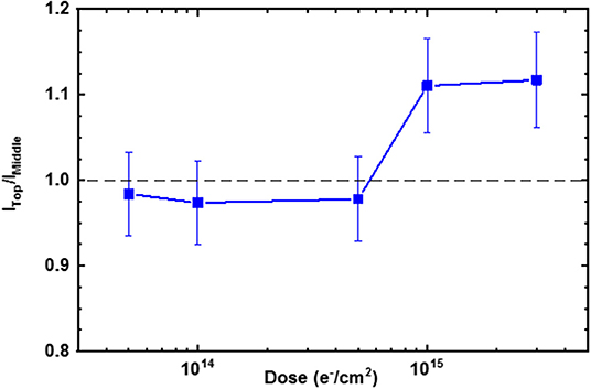
Figure 4. Ratio between the current of the top subcell (ITop) and middle subcell (IMiddle) as calculated from EQE spectral measurements as a function of the electron irradiation doses.
From these elements, we can infer the behavior of each subcell component and their influence to the operation of the whole device.
The top subcell is found very robust against irradiation (Table 3): we observe that current losses still remain within 5% for highest doses. Moreover, the changes of the correlated spectral response are much less marked than those of the other subcells.
Conversely, the middle subcell is, as expected, highly susceptible to irradiation. This is strongly marked by the EQE curves (Figure 2B), having maxima values between 700 and 900 nm: in more irradiated devices spectral response significantly degrades at longer wavelengths. This behavior is present from low doses, but it becomes much more evident for heavy irradiation (Figures 2B, 4). This strong degradation of the middle junction confirms that it becomes the current-limiting subcell when irradiation doses increase. This can be further pointed out by exploiting the recently proposed experimental technique, which allows us to directly evaluate the limiting subcell as a function of the irradiation dose [29]. We associate this behavior of the middle junction to the physical mechanisms inside the considered p – n middle junction (Figure 1A). Namely, the long wavelength part of the EQE middle-subcell curve corresponds to the low-energy photons, which are absorbed by the base layer of the considered subjunction. These photons produce carriers which have to pass through the whole junction to be collected. As irradiation-induced defects are known to cause a decrease of the diffusion length with the increasing of the dose, the photogenerated carriers have a higher probability to be recombined [30], so reducing the spectral efficiency in the long-wavelength region. Beyond this physical interpretation, we note that Isc decreases of about 20% (Table 3), making the middle subcell the most sensitive to the irradiation and degradation process.
Finally, the bottom subcell is confirmed to degrade more than the top subcell and less than the middle one, as expected [2, 5, 7, 31]. The spectral response curves (Figure 2B) indicate that irradiation particularly affects the short-wavelength part of the spectrum, i.e., the region between approximatively 950 and 1200 nm.
Proton Irradiation
Similarly to the electron irradiation, for proton-irradiation experiments we measured a bunch of 30 CTJ30-80 thin cells. Six sets of 5 cells have been prepared; each set is irradiated with given dose of radiations, i.e., 1 × 10¹⁰, 2 × 10¹⁰, 5 × 10¹⁰, 1 × 10¹¹, and 3 × 10¹¹ p+/cm2. All the sets undergoes particles with energy of 1 MeV. Again, 2 cells of each 5 cell set are used for the here considered irradiation tests, while 3 of them are subjected to different feasibility tests. Similarly to the electron case, 3 measurements are accomplished on each irradiated sample, whose values are averaged; for each dose, the reported measurement is the average of the response of 2 samples.
Six particle doses are here considered, other than the five doses of the previously discussed electron irradiation. Electric performance and spectral response are measured on two cells for each irradiation dose, so obtaining 12 tested devices. Similarly to the electron irradiation case, I–V and spectral EQE measurements are carried out, where the calculation of the remaining factors and their comparison with the standard CTJ30 thick cells allow us to immediately provide a comprehensive landscape of the proton-irradiated CTJ30-80 performance. The experimental data are shown in Plots Figures 5A,B.
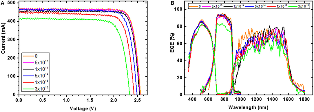
Figure 5. (A) I–V curves and (B) spectral responses of the thin cells in BOL and EOL configurations. The doses are given in p+/cm2 units. Note that the experimental noise grows from top to bottom junction.
The averaged I–V curves and electric parameters of the proton-irradiated EOL cells are reported in Figure 5A and Table 4, respectively, while the correlated EQE spectral response curves are depicted in Figure 5B.
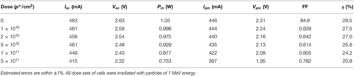
Table 4. Averaged electric performance (at 25°C) of the BOL and proton-irradiated EOL cells.
The summary of the averaged electric responses reported in Table 4 for both BOL and EOL cells, analogously to what previously reported in Table 1 for electron-irradiated cells, where Isc and Voc, Pm, Ip, and Vpm, FF, and η are defined as in the previous Table 1. The estimated relative error is the same as in the electron case.
The remaining factors of the considered samples are shown in Figure 6a and in Table 5 as a function of their respective irradiation doses. The remaining factors of proton-irradiated standard 140-μm-thick CTJ30 cells, on the other hand, are shown in Figure 6b (employing the 1 MeV energy), while results of the tests on those cells with different proton energies are discussed in Campesato et al. [23]. The comparison between thin and thick devices points out that, similarly to the case of electron irradiation (Figure 3), the response to irradiation of CTJ30-80 samples is very similar to that of the standard CTJ30 cells.
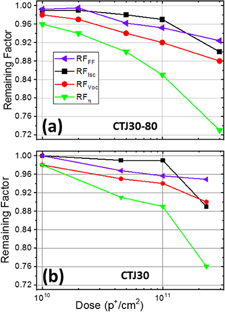
Figure 6. Remaining factors of Isc, Voc, FF, η as a function of the proton irradiation dose: comparison between the trend of (a) the here discussed (thin) CTJ30-80 devices and (b) the (thick) CTJ30 devices.
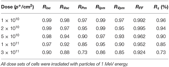
Table 5. Remaining factors of the electric performance of proton-irradiated cells for each particle dose.
Actually η is the most degraded parameter, as for the electron irradiation. In particular Figure 6a highlights a critical proton irradiation dose at 5 × 10¹⁰ p+/cm2 roughly, after which all the remaining factors dramatically drop down. We guess that this decreasing is likewise due to the change of the limiting function such as in the electron irradiation case. In fact, similarly to electrons, for low irradiations the device is still top-limited. Conversely, the slow decrease of performance until 5 × 10¹⁰ p+/cm2 pointed out by I–V measurements, is followed at 1 × 10¹¹ p+/cm2 by a marked decrease. We associated such an evolution to the fact that the middle subcell is becoming the current-limiting one.
We can here evaluate the contribution of each subcell to the global behavior under proton irradiation. Actually, the spectral responses in Figure 5B point out that the lower energy protons produce the most severe damage in the top subjunction; conversely, the middle subcell shows negligible changes. When the proton energy is increased, the damage progressively affects the deeper layers of the cell structure. In particular the middle subcell undergoes the worst damage by the 1 MeV protons, which we estimate to enter in the middle subjunction with an energy of ≃0.9 MeV and, after passing it, arriving on the bottom subcell with an energy of ≃0.7 MeV; protons with higher energies (e.g., 10 MeV) affect the substrate only and seem to not deteriorate the active layers [23].
We employ the same procedure as in the electron case (Table 3): the subcell degradation is estimated by calculating Isc from EOL spectral response and their ratios with respect to the BOL values, whose results are reported in Table 6. We note that, taking into account the different considered irradiation doses, the overall behavior of the subcells irradiated with protons is very similar to that of electron irradiation, as expected by works in similar conditions on similar multi-junction cells [12, 32, 33]. In Figure 7 the ratio between the currents, calculated from the spectral measurements, of the top and middle subcells is depicted. The plot shows that this ratio becomes larger than 1 around a dose of 5 × 10¹⁰ p+/cm2, confirming that the middle-subcell becomes the limiting one above this irradiation dose, in agreement with I–V curves (Figure 6a).
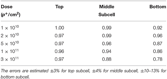
Table 6. Ratios between short-circuit currents of BOL and EOL subcells calculated from EQE measurements for different 1 MeV proton fluencies.
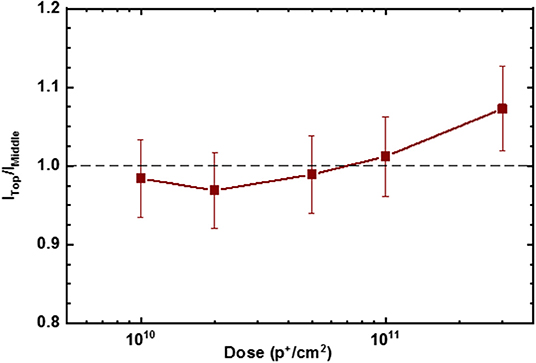
Figure 7. Ratio between the current of the top subcell (ITop) and middle subcell (IMiddle) as calculated from EQE spectral measurements as a function of the proton irradiation doses.
Namely, EQE spectral measurements highlight the expected strong degradation of middle subjunction (Figure 5), confirming this phenomenon. With proton, the bottom subjunction is degrading more than with electrons, as reported in Table 6.
Results: Photoluminescence Spectra
It is known that irradiation causes deep point defects which produces a decreasing of the obtained current due to carrier recombination [5]. Information about the point defects induced by irradiation can be obtained by exploiting suitable techniques. In the considered case we carried out specific photoluminescence experiments with the above described equipments. For such kind of measurements, we focus on the InGaP and InGaAs junctions. Actually, applying PL technique on multi-junction cells gives rise to problems in exciting one selected junction and distinguishing the spectral contribution of each subcell. Therefore, PL experiments are here accomplished on samples specifically prepared with this aim. They are single-junction cells which have been prepared by CESI with the standard CTJ30-80 cell protocol. They have a 2 × 2 cm2 size, with a protective layer of InGaP on the top and an active junction of either InGaP or InGaAs, all grown on Ge substrate identically to standard multi-junction CTJ30-80 cells. The employed growth technique provides high-quality highly-optimized samples, where lattice mismatch at the interfaces between the different layers is absent as in the multi-junction cell growth. We therefore reasonably assume that each single junction deposited on Ge substrate exhibits the same luminescent response of the subjunction embedded in the three-junction device, in particular with respect to the qualitative PL analysis [34].
We accomplish measurements on both BOL and EOL samples, which have been irradiated with the same particles and doses of the complete junctions. PL experiments are accomplished at room temperature (300 K) in order to test the materials in the same conditions of the EQE and I–V experiments.
In Figure 8 the room-temperature PL spectra of the InGaP junction, in BOL, electron-irradiated EOL and proton-irradiated EOL are shown. A unique peak is evidenced, which is centered around the energy gap of InGaP (≃1.85 eV) as indicated by the literature [35]: we therefore reasonably associate it to this band-to-band transition. It is worth noting that the FWHM of BOL curve is 84 meV, while that of EOLs is 105 meV for electron-irradiated and 96 meV for proton-irradiated. We note that the BOL peak shows a doubled intensity and a lower full-width-half-maximum (FWHM) with respect to the EOL ones: this is in qualitative agreement with the electric measurements previously discussed in sections Electron Irradiation and Proton Irradiation. Actually, we reasonably associate the absence of new peaks, the increase of FWHM, and the decrease of the overall PL intensity in EOL samples to an increment of non-radiative recombination processes, which are known to negatively affect the material performance in a PV device.
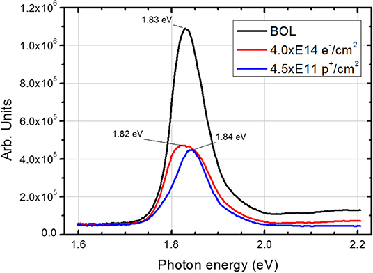
Figure 8. PL spectra of InGaP junction in BOL, EOL electron-irradiated and EOL proton-irradiated conditions at room temperature.
In Figure 9 the PL spectra of the InGaAs junction, in BOL, electron-irradiation and proton-irradiation EOL, along with the related Gaussian deconvolutions are shown. In this case, the emission intensity of EOL samples is 500 times lower than that of BOL sample, in agreement with the literature [36]: this confirms the very higher sensitivity to irradiation of the InGaAs junction with respect to the InGaP one.
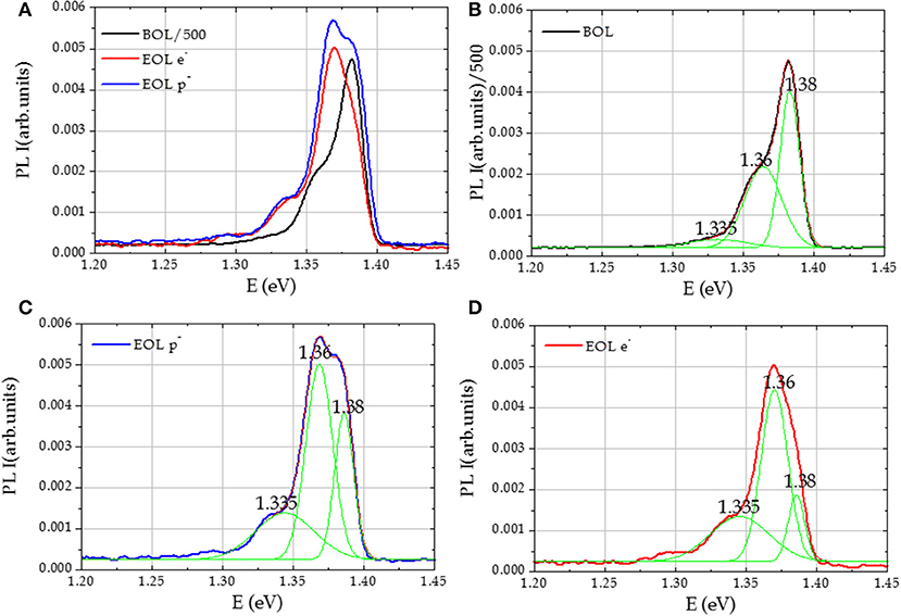
Figure 9. PL spectra of (A) InGaAs junction in BOL, EOL electron-irradiated and EOL proton-irradiated conditions at room temperature and correlated Gaussian deconvolutions of (B) BOL, (C) proton-irradiated EOL, and (D) electron-irradiated EOL.
Specifically, the BOL emission (black curve) is the superimposition of three different emission peaks: the first one (Mb−b) is compatible with an expected energy gap at 1.38 eV (band-to-band transition at room temperature) [37], while the second one (M2) is centered at 1.36 eV. Such an emission is associated to a specific structure, protected by trade secret, which has been introduced in the InGaAs thin films in order to increase photon absorption at low energies. The attribution of the third peak (M3) at 1.335 eV, wider and with lower intensity, is still under investigation. According to the Gaussian deconvolutions also reported in Figure 9 proton irradiation produces a decrease of the band-to-band transition at 1.38 eV, which is much more pronounced in the case of electron irradiation, in agreement with electrical characterization.
These results indicate that InGaAs is intrinsically more susceptible to irradiation damage than InGaP. According to the literature, we associate this behavior to a deterioration of the minority carrier diffusion length [5, 31].
Conclusions
Our systematic investigation on electron and proton irradiated triple-junction thin InGaP/InGaAs/Ge solar cells has examined 80-μm-thick mechanically flexible solar devices, specifically designed for space applications. Their operative features have been evaluated through electric and spectral response measurements as a function of particle irradiation reproducing their working conditions. The investigation of different doses has enabled to obtain a qualitative description of the produced radiative point defects of top InGaP and middle InGaAs subcells. Comparative measurements on begin-of-life and end-of-life cells have allowed to highlight the specific irradiation-correlated features and, in particular, the performance degradation as a consequence of the particle bombardment. The exploited specific figure of merit of remaining factors has been able to quantitatively depict the performance degradation of the whole multi-junction solar device as a function of the irradiation doses.
We have carried out a fine analysis of each single subjunction, whose spectral responses as a function of the irradiation have allowed to estimate the current produced by each single subcell. These data have been compared with the electric responses of the overall device in order to point out the evolution of the current-limiting-junction. These experiments have pointed out that in the present 80-μm-thin configuration the middle InGaAs subcell is the most radiation-damageable junction: actually the most marked degradation in PV performance is associated to the change of the current-limiting subcell from the top to the middle one, both for electron and proton irradiation. Such a behavior, which is confirmed both by electric and photoluminescence measurements, is analogous to what previously demonstrated in thick 3-junctions solar devices. Conversely, in top InGaP subcells component of the considered device, the irradiation-induced changes have been very low (few %), so as not to compromise electric, spectral, and photoluminescence features. Finally, in electric performance of bottom Ge subcell component some damages correlated with irradiation can be found, but less marked then in middle subjunction when irradiated with electrons while the remaining factors are worse when irradiated with protons. PL analyses of top and middle junctions irradiated with electrons and protons show a decrease in radiative lifetimes as expected, with the introduction of non-radiative centers.
It is worth comparing these operative features with those of the usual available multi-junction space solar cells. If we consider the performance and response to the irradiation, the good resistance of CTJ30-80 devices is roughly the same as that of standard devices. The main differences can be found in the high produced power, low-weight, and bendable structure. Namely, it is worth noting that the typical specific power of this class of a solar devices lies around 0.5 W/g [3]; here, although the radiation resistance and the electric performance are approximately the same, the specific power is doubled. On the other hand, the relatively low bending radius of 30 mm strongly increases the usual adaptability to the spacecrafts of the whole class of these solar devices [14, 15].
Summarizing, the considered thin InGaP/InGaAs/Ge configuration has displayed a radiation resistance analogous to that of the devices with standard thickness. Their mechanical flexible configuration enables to add more freedom to the design of new spacecrafts; on the other hand, the very high specific power allows to obtain, for the same amount of power, lighter solar devices, giving a contribution for limiting costs in space missions. These advantages are achieved, we have demonstrated, still maintaining a good resistance to particle irradiation, confirming that the considered thin cells as a valid option for the application in space uses.
We can note that the basic advantage of this kind of solar cells is the weight savings of spacecrafts, produced power being the equal, where they are installed: this allows a decreasing of the coasts of putting them into orbit. On the other hand, this class of solar devices potentially opens a more innovative pathway in the design of satellites: actually their flexibility allows to exploit greater degrees of freedom in the general design of the space, enabling a more optimized planning of each spacecraft component.
Data Availability Statement
The datasets generated for this study are available on request to the corresponding author.
Author Contributions
JP and SB conceived the experiments, interpreted the data, and coordinated the research. FA carried out the I–V and spectral EQE measurements. AL carried out PL experiments and correlated data interpretation. RC, MC, and EG conceived and prepared the samples.
Conflict of Interest
RC, MC, and EG are employed by company CESI which produces and markets the studied multi-junction solar cells. All other authors declare no competing interests.
Acknowledgments
This work was partially supported by the ESA project Industrialization and Qualification of CTJ30-Thin solar cells. Thanks also to ASI for supporting this activity.
References
1. El Chaar L, Iamont LA, El Zein N. Review of photovoltaic technologies. Renew Sustain Energy Rev. (2011) 15:2165–75. doi: 10.1016/j.rser.2011.01.004
2. Hegedus S, Luque A. Handbook of Photovoltaic Science and Engineering. 2nd ed. Chichester: Wiley (2011).
3. Bett AW, Philipps SP, Essig S, Heckelmann S, Kellenbenz R, Klinger V, et al. Overview about technology perspectives for high efficiency solar cells for space and terrestrial applications. In: Proc. 28th EU PVSEC. Paris (2013).
4. Yamaguchi M, Ando K. Mechanism for radiation resistance of InP solar cells. J Appl Phys. (1988) 63:5555. doi: 10.1063/1.340332
5. Yamaguchi M. Radiation-resistant solar cells for space use. Solar Energy Mater Solar Cells. (2001) 68:31–53. doi: 10.1016/S0927-0248(00)00344-5
6. Yi T, Lu M, Yang K, Xiao P, Wang R. Electroluminescence analysis of injection-enhanced annealing of electron irradiation-induced defects in GaInP top cells for triple-junction solar cells. Nucl Instr. Methods Phys Res B. (2014) 335:66–9. doi: 10.1016/j.nimb.2014.06.006
7. Makham S, Sun GC, Bourgoin JC. Modelling of solar cell degradation in space. Solar Energy Mater Solar Cells. (2010) 94:971–8. doi: 10.1016/j.solmat.2010.01.026
8. Lee HS, Yamaguchi M, Ekins-Daukes NJ, Khan A, Takamoto T, Imaizumi M, et al. Effects of a low-energy proton irradiation on n+/p-AlInGaP solar cells. Physica B. (2006) 376–7:564–7. doi: 10.1016/j.physb.2005.12.142
9. Makham S, Zazoui M, Sun GC, Bourgoin JC. Non-empirical prediction of solar cell degradation in space. Semicond Sci Technol. (2005) 20:699–704. doi: 10.1088/0268-1242/20/8/008
10. Dharmarasu N, Yamaguchi M, Khan A, Takamoto T, Ohshima T, Itoh H, et al. Low-energy proton-induced defects in n+ /p InGaP solar cells. Solar Energy Mater Solar Cells. (2003) 75:327–33. doi: 10.1016/S0927-0248(02)00176-9
11. Lee HS, Yamaguchi M, Ekins-Daukes NJ, Khan A, Takamoto T, Agui T, et al. Deep-level defects introduced by 1 MeV electron radiation in AlInGaP for multijunction space solar cells. J Appl Phys. (2005) 98:093701. doi: 10.1063/1.2115095
12. Dharmarasu N, Khan A, Yamaguchi M, Takamoto T, Ohshima T, Itoh H, et al. Effects of proton irradiation on n+p InGaP solar cells. J Appl Phys. (2002) 91:3306. doi: 10.1063/1.1445276
13. Baca AJ, Yu KJ, Xiao J, Wang S, Yoon J, Ryu JH, et al. Compact monocrystalline silicon solar modules with high voltage outputs and mechanically flexible designs. Energy Environ Sci. (2010) 3:208–11. doi: 10.1039/b920862c
14. Lipomi DJ, Bao Z. Stretchable, elastic materials and devices for solar energy conversion. Energy Environ Sci. (2011) 4:3314–28. doi: 10.1039/c1ee01881g
15. Kaltenbrunner M, White MS, Głowacki ED, Sekitani T, Someya T, Sariciftci NS, et al. Ultrathin and lightweight organic solar cells with high flexibility. Nat Commun. (2012) 3:770. doi: 10.1038/ncomms1772
16. Gibb J. Lightweight Flexible Space Solar Arrays, Past, Present and Future. In: 2018 IEEE 7th World Conference on Photovoltaic Energy Conversion (WCPEC) (A Joint Conference of 45th IEEE PVSC, 28th PVSEC 34th EU PVSEC). Waikoloa Village, HI (2018). p. 3530–4. doi: 10.1109/PVSC.2018.8547918
17. Dutta P, Rathi M, Khatiwada D, Sun S, Yao Y, Yu B, et al. Flexible GaAs solar cells on roll-to-roll processed epitaxial Ge films on metal foils: a route towards low-cost and high-performance III-V photovoltaics. Energy Environ Sci. (2019) 12:756–66. doi: 10.1039/C8EE02553C
18. Gori G, Campesato R. Photovoltaic cell having a high conversion efficiency. In: PCT, I09111-WO (2009).
19. Gori G, Campesato R. Thin and flexible triple junction cells 30% efficient: qualification results and future space applications. In: 44th PVSC. Washington DC: IEEE (2017). doi: 10.1109/PVSC.2017.8366087
20. Campesato R, Gori G, Casale M, Gabetta G. Radiation effects on advanced multi junction solar cells for space applications. In: 32nd EU PVSC. Munich (2016).
21. Campesato R, Greco E, Casale M, Gori G. NIEL DOSE analysis on triple junction cells 30% efficient and related single junctions. In: 44th PVSC. Washington DC: IEEE (2017). doi: 10.1109/PVSC.2017.8366088
22. Imaizumi M, Nakamura T, Takamoto T, Ohshima T, Tajima M. Radiation degradation characteristics of component subcells in inverted metamorphic triple-junction solar cells irradiated with electrons and protons. Prog Photovolt Res Appl. (2017) 25:161–74. doi: 10.1002/pip.2840
23. Campesato R, Casale M, Gabetta G, Gori G. Electron and proton irradiation on high efficiency III-V solar cells based on three and four junctions. In: 28th EU PVSC. Paris (2013).
24. Burdick J, Glatfelter T. Spectral response and I-V measurements of tandem amorphous-silicon alloy solar cells. Solar Cells. (1986) 18:301–14. doi: 10.1016/0379-6787(86)90129-8
25. Meusel M, Adelhelm R, Dimroth F, Bett AW, Warta W. Spectral mismatch correction and spetrometric characterization of monolithic III-V multi-junction solar cells. Prog Photovolt Res Appl. (2002) 10:243–55. doi: 10.1002/pip.407
26. Peharz G, Siefer G, Bett AW. A simple method for quantifying spectral impacts on multi-junction solar cells. Solar Energy. (2009) 83:1588–98. doi: 10.1016/j.solener.2009.05.009
27. Holovský J, Bonnet-Eymard M, Boccard M, Despeisse M, Ballif C. Variable light biasing method to measure component I-V characteristics of multi-junction solar cells. Solar Energy Mater Solar Cells. (2012) 103:128–33. doi: 10.1016/j.solmat.2012.04.014
28. Meusel M, Baur C, Létay G, Bett AW, Warta W, Fernandez E. Spectral response measurements of monolithic CaInP/Ga(In)As/Ge triple-junction solar cells: measurement artifacts and their explanation. Prog Photovolt Res Appl. (2003) 11:499–514. doi: 10.1002/pip.514
29. Arcadi F, Parravicini J, Campesato R, Casale M, Greco E, Binetti S. Measurement of the limiting subcell in multi-junction space solar devices by restricted-wavelength-range illumination. Prog Photovolt Res Appl. (2018) 26:942–8. doi: 10.1002/pip.3018
30. Pons D, Bourgoini JC. Irradiation-induced Defects in GaAs. J Phys C Solid State Phys. (1985) 18:3839–71. doi: 10.1088/0022-3719/18/20/012
31. Dimroth F. High-efficiency solar cells from III-V compound semiconductors. Phys Stat Solidi. (2006) 3:373–9. doi: 10.1002/pssc.200564172
32. Yamaguchi M. Radiation resistance of compound semiconductor solar cells. J Appl Phys. (1995) 78:1476. doi: 10.1063/1.360236
33. Dharmarasu N, Yamaguchi M, Khan A, Yamada T, Tanabe T, Takagishi S, et al. High-radiation-resistant InGaP, InGaAsP, and InGaAs solar cells for multijunction solar cells. Appl Phys Lett. (2001) 79:239. doi: 10.1063/1.1409270
34. Le Donne A, Acciarri M, Gori G, Colletto R, Campesato R, Binetti S. Optical and electrical characterization of AlGaInP solar cells. Solar Energy Mater Solar Cells. (2010) 94:2002–6. doi: 10.1016/j.solmat.2010.06.001
35. Kondow M, Minagawa S, Inoue Y, Nishino T, Hamakawa Y. Anomalous temperature dependence of the ordered Ga0.5In0.5P photoluminescence spectrum. Appl Phys Lett. (1989) 54:1760. doi: 10.1063/1.101283
36. Zheng Y, Yi T, Wang J, Xiao P, Wang R. Radiation damage analysis of individual subcells for GaInP/GaAs/Ge solar cells using photoluminescence measurements. Chinese Phys Lett. (2017) 34:026101. doi: 10.1088/0256-307X/34/2/026101
Keywords: multi-junction cells, irradiated cells, component cells, III-V semiconductors, space solar cells
Citation: Parravicini J, Arcadi F, Le Donne A, Campesato R, Casale M, Greco E and Binetti S (2019) Effect of the Irradiation on Optical and Electrical Properties of Triple-Junction Flexible Thin Solar Cells for Space Applications. Front. Phys. 7:169. doi: 10.3389/fphy.2019.00169
Received: 09 July 2019; Accepted: 11 October 2019;
Published: 01 November 2019.
Edited by:
Samit K. Ray, Indian Institute of Technology Kharagpur, IndiaCopyright © 2019 Parravicini, Arcadi, Le Donne, Campesato, Casale, Greco and Binetti. This is an open-access article distributed under the terms of the Creative Commons Attribution License (CC BY). The use, distribution or reproduction in other forums is permitted, provided the original author(s) and the copyright owner(s) are credited and that the original publication in this journal is cited, in accordance with accepted academic practice. No use, distribution or reproduction is permitted which does not comply with these terms.
*Correspondence: Simona Binetti, c2ltb25hLmJpbmV0dGlAdW5pbWliLml0
†Present address: Francesco Arcadi, Arca Polimeri s.r.l., Ceriano Laghetto, Italy