 Kazunori Takahashi
 Kengo Hanaoka
- Department of Electrical Engineering, Tohoku University, Sendai, Japan
A frequency-tuned radiofrequency (rf) plasma source is automatically controlled to minimize the rf power reflection and to maintain the constant net rf power corresponding to the forward power minus the reflected power. The experiment is performed with a power amplifier operational for the frequency of 37–43 MHz, a compact helicon source consisting of a loop antenna, a solenoid, and an insulator tube. The rf power is supplied to the rf antenna via an impedance matching circuit consisting of only fixed small ceramic capacitors. It is demonstrated that the reflection coefficient of the rf power is minimized within ~10 ms, and the net power is successfully maintained at a constant level.
Introduction
Radiofrequency (rf) plasma source operated in the frequency of 1–100 MHz has been widely used for various applications such as industrial plasmas [1, 2], space propulsion devices [3, 4], and fusion plasmas [5]. To transfer the rf power to a load, the load impedance has to be matched to the output impedance of the generator and the characteristic impedance of a power transmission line, being typically 50 Ω. The impedance matching is generally performed by inserting two variable capacitors and an inductor (if necessary), where the capacitances are adjusted by mechanical motion.
Fundamental studies on and development of space propulsion devices utilizing the rf plasma sources have vigorously progressed in recent years [6–11]. Since the weight and size of the rf system mountable on the spacecraft is very limited, development of the compact rf system is required for the rf plasma thruster. Further addressing space propulsion, the time lag of the communication between the spacecraft and the ground control station would be a serious problem for the impedance matching. Therefore, automatic and fast control of the impedance tuning is useful for further development of the rf plasma thruster.
The compact, automatically controlled, and fast-controlled rf plasma system is also useful for terrestrial industrial plasma devices such as plasma sputtering and etching reactors in a recently developed new concept of the semiconductor manufacturing system, being called “Minimal Fab” [12, 13]. In the traditional semiconductor manufacturing system, the diameter of the silicon wafer has been increased to yield sufficient economic benefit by low-mix high-volume production in the large-scale manufacturing system (called “Mega Fab”). On the other hand, Minimal Fab consists of various manufacturing tools in processing a half-inch wafer. Since the wafer is transferred between the processing tools in a localized clean wafer transfer system, no clean room is required for the device production; the facility and production costs can be reduced for the high-mix and low-volume products. The frame and wafer transfer structures are strictly standardized to connect the processing tools. Therefore, all of the components required for each tool, e.g., a plasma reactor, a pumping system, an rf generator, the wafer transfer mechanics, and the programmable logic controller, and so on, have to be contained within the compact frame. Furthermore, the precise control of the pulsed plasma would also be required for some plasma processing methods, e.g., plasma etching by Bosch process [14], where gas species are alternatively switched for etching and passivation.
As described above, the available space for the rf system is strictly limited in the applications; hence, the development of the compact rf system for the plasma source is a significantly important technology. To overcome this issue, a frequency-variable tuning has been tested in several laboratory experiments. Charles et al. has used the frequency-variable power generator operated at around 13.56 ± 0.678 MHz with the fixed small ceramic capacitors for impedance tuning [15]. One of the authors has used an amplifier operational for the broader range of the frequency to match the impedance for the industrial plasma source [16], where the frequency was manually adjusted for the initial laboratory test. These experiments have been performed with the linear rf amplifier classified as class AB, while class D or class E switching amplifiers have also been used for the frequency-tunable matching [17–20]. The traditional impedance matching technique can perform nearly perfect impedance matching by adjusting two capacitors, while it would be difficult to obtain the zero power reflection for the frequency tuning since only one control parameter (frequency) is adjustable. Since the primary parameter deciding the plasma characteristics in terms of the rf system would be the net power given by the forward power minus the reflected power, it would be favorable to maintain the constant net power during plasma production rather than the forward power when the perfect impedance matching is difficult.
The aim of the present study is to develop a compact, automatic, and fast-controlled rf system for future applications of the rf plasma source to the terrestrial plasma processing tools in “Minimal Fab” and the space propulsion device called a helicon thruster. By mounting an autonomously operational controller in the rf system, frequency tuning for the impedance matching and power control for maintaining the constant net rf power, which corresponds to the forward power minus the reflected power, are simultaneously performed. Details of the rf system providing the impedance tuning within about 10 ms is described here.
Experimental Setup
Figure 1A shows the schematic diagram of the plasma reactor used for the present experiment, which is very similar to that of the previous experiment [16]. The experiment is performed with a weakly magnetized rf plasma source attached to a 114 mm3 vacuum chamber, which is evacuated by a 70-l/s turbomolecular pump to a base pressure of about 10−4 Pa. The source consists of a 50-mm-outer-diameter, 42-mm-inner-diameter, and 75-mm-long ceramic source tube wound by a double-turn rf loop antenna and a solenoid providing a static magnetic field. The solenoid is situated at z = −15 mm, and dc current of IB = 4.5 A is supplied to the solenoid from a dc power supply, providing a magnetic field strength of about 45 G at the solenoid center, where the open source exit is defined as z = 0. The rf loop antenna consisting of a 4-mm-diameter copper tube is wound at z = −50 ± 10 mm, where the antenna radius is about 27 mm. The upstream side of the ceramic tube is terminated at z = −75 mm by a grounded vacuum flange having a gas injection port and a small viewport. Argon gas is introduced from the gas injection port via a mass flow controller, and the gas flow rate is maintained at 10 sccm, giving the chamber pressure of about 0.65 Pa, which is measured by an ionization gauge attached to the side flange of the chamber. The rf antenna is powered by a broadband class AB rf amplifier via an impedance matching circuit consisting of only fixed ceramic capacitors (C1 and C2) as drawn in Figure 1B; the argon plasma is produced inside the source tube. Rp, Lp, Ra, and La in Figure 1B are the plasma resistance, plasma inductance, antenna resistance, and antenna inductance, respectively, which will be discussed for the matching network design in “Design of Matching Network.” Figure 2 shows the photograph of the source, including the impedance matching circuit; the matching circuit can be made very compact as shown in the photograph of Figure 2 as it does not contain the variable capacitors. To reduce the power loss at the capacitors, high-Q and ultra-low equivalent series resistance capacitors (HQCC series of AVX Corporation) are mounted on the circuit. The plasma source structure and the matching circuit are air-cooled by using a 40-mm-diameter small fan; it is confirmed that the plasma source can be operated in steady state (at least for 20–30 min in the laboratory experiment) for 200 W rf power. It should be noted that a similar previous experiment has shown plasma density of about 1018 m−3 for the rf power of about 100 W [16]. An optical emission intensity Iopt is measured by a photodetector via an optical fiber connected to the viewport of the upstream flange to very roughly know the relative plasma density.
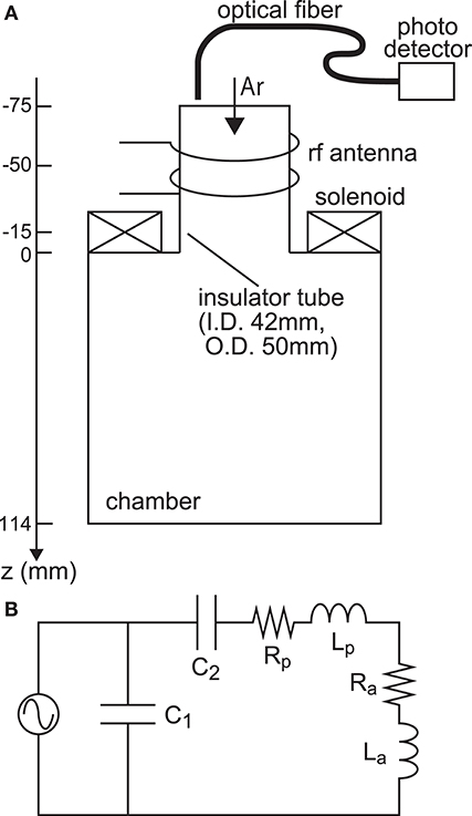
Figure 1. (A) Schematic diagram of a weakly magnetized rf plasma source attached to the 114 mm3 vacuum chamber. (B) Schematic of an impedance matching circuit containing a plasma resistance Rp and a plasma inductance La, where C1 and C2 are chosen as 390 and 73 pF, respectively. La and Ra are the antenna inductance and resistance, respectively.
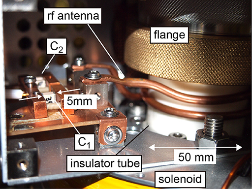
Figure 2. Photograph of the plasma source and the impedance matching circuit consisting of the fixed ceramic capacitors.
Figure 3 shows the schematic diagram of the presently developed rf system. An rf signal from a voltage-controlled oscillator (VCO) is input into a voltage variable attenuator (VVA) and further input into a 200-W class AB rf power amplifier (AMP) operational between 37 and 43 MHz. Both the output impedance of the amplifier and the coaxial cables are 50 Ω. It should be noted that the dc–rf conversion efficiency of the power amplifier is about 75%; the bandwidth of the amplifier is limited to 37–43 MHz to ensure the conversion efficiency. The amplified rf power is transferred to a load via a bi-directional coupler (50 ± 0.5 dB coupling and 20 dB directivity). The rf signals coupled with the forward and reflected powers are converted into dc voltages by using zero-bias schottky diode rf detectors and low-pass filters (LPFs); then, the absolute value of the reflection coefficient |Γr| given by
can be calculated. The driving frequency and the output power can be controlled by the voltage signals to the VCO and the VVA. To autonomously control both the frequency and the rf power, a CompactRIO Single-Board Controller (National Instruments, sbRIO-9637) is mounted on the system. The controller includes the Linux Real-Time operating system (OS), field-programmable gate array (FPGA), analog–digital (AD) converters, and digital–analog (DA) converters; it has ports of the digital input/output (DIO), analog input (AI), and analog output (AO). The voltage signal to the VCO and the VVA can be controlled by the AO channels, and the dc voltage corresponding to the forward and reflected powers are monitored by the AI channels, where the DIO channels are used to control the RF on/off and to monitor some signals from the thermal interlock. Since the CompactRIO Single-Board Controller has the OS, it can autonomously operate even if a personal computer (PC) is disconnected. The detailed procedure of the autonomous control is described in the “Results.”
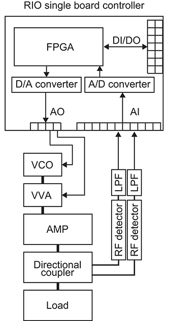
Figure 3. Schematic diagram of the rf system containing a board controller including the FPGA and the AD/DA converters.
Design of Matching Network
Since it is difficult to perfectly match the load impedance to the output impedance of the rf amplifier for the frequency tuning system as described in “Introduction,” it is significantly important to select proper capacitors in the matching network. Many modeling studies have been performed to characterize the electrical property of the rf plasma source over the wide range of parameters [21]. However, the very simple equivalent circuit shown in Figure 1B is used here to explore the suitable capacitances for the matching network since the detailed model strongly depends on the specification of the plasma source. The total impedance ZL of the matching circuit including the plasma in Figure 1B is given by
The reflection coefficient given by Equation (1) can be rewritten as
where Z0 is the output impedance (50 Ω) of the amplifier being equal to the characteristic impedance of the coaxial cable connecting the amplifier and the matching network. One of the experiments measured the resistance and the reactance of the load including the rf antenna and the plasma for the inductively coupled plasma source [22], where the equivalent circuit is very similar to Figure 1B. The results showed the plasma resistance of about a few ohms, which is higher than the typical circuit resistance of an order of 10−1 Ω. Furthermore, the reactance is mostly unchanged or decreases a fraction with an increase in the discharge power; it can be considered that the plasma reactance is much smaller than the antenna reactance (L ~ La). The inductance of the N-turn antenna having the radius a and the axial length l is generally given by
where μ0 is the vacuum permeability. Kn is the Nagaoka coefficient given by [23]
where K(k) and E(k) are the complete elliptic integrals of the first and second kind, respectively. The numerically calculated inductance for the given antenna geometry of l = 20 mm, a = 27 mm, and N = 2 is La ~ 0.235 μH. The two capacitors in Figure 1B are chosen so as to have a minimum value of |Γr| within the frequency range of 37–43 MHz and nearly zero value of |Γr| for R of a few ohms.
Figure 4A shows the typical calculation of |Γr| as a function of the frequency for various values of R, where C1 = 390 pF, C2 = 73 pF, and L = 0.235 μH are used. It is found that the nearly zero value of |Γr| can be obtained for R = 2 Ω at the frequency of ~40 MHz. It should be noted that a slight decrease in |Γr| at ~ 40 MHz is still obtained for R = 0.25 Ω case, which would be enough to ignite the discharge.
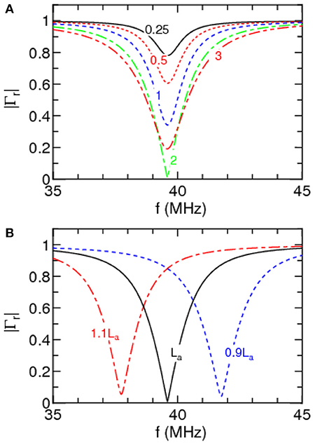
Figure 4. (A) Reflection coefficient |Γr| calculated by Equation (5) as a function of the frequency for various values of the resistance R, where C1 = 390 pF, C2 = 73 pF, and the antenna inductance La ~ 0.235 μH calculated by Equation (6) are used for the calculation. (B) Reflection coefficient for R = 2 Ω when changing the antenna inductance by ± 10 % of the La used in (A).
For the high frequency above 10 MHz, the reactance is significantly changed by the geometrical error of the antenna, the parasitic capacitance and inductance in the circuit. Figure 4B shows the calculated |Γr| for the R = 2 Ω cases with the inductances of La and La ± 10 %. The frequency giving the minimum |Γr| is found to be shifted by the change of the inductance. Therefore, the measurement of the reflection coefficient by a vector network analyzer is required to be performed, whereby the values of the capacitance should be adjusted. However, the above-mentioned design procedure is useful to roughly estimate the capacitors in the matching network.
Results
Before showing the automatic and fast control of the frequency tuning rf system, the basic characteristics of the loads without and with the plasma are shown. Figure 5A shows the reflection coefficient |Γr| as a function of the rf frequency. The data plotted by crosses and filled circles are taken with no gas (no plasma) and with argon flow rate of CAr = 10 sccm and solenoid current of IB = 4.5 A, respectively. It is noted that the voltage signals to the VVA are maintained at a constant level, and the data are taken by changing the voltage signal to the VCO, i.e., the rf frequency. The optical emission intensity Iopt, forward rf power Pf, and reflected rf power Pr measured for CAr = 10 sccm and IB = 4.5 A are plotted by filled circles in Figure 5B and by open circles and filled squares in Figure 5C, respectively. The net power Pnet is simply calculated by Pnet = Pf – Pr and plotted by crosses in Figure 5C. The optical emission intensity shows that plasma can be produced for the frequency range of 39.5–42 MHz.
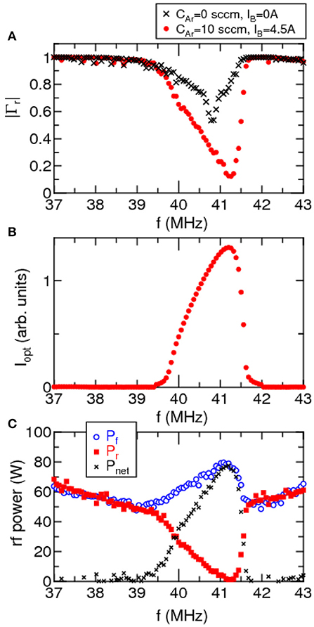
Figure 5. (A) Measured reflection coefficient |Γr| as a function of the rf frequency for CAr = 0 sccm and IB = 0 A case (crosses) and for CAr = 10 sccm and IB = 4.5 A case (filled circles). (B) The optical emission intensity Iopt measured from the viewport on the upstream flange. (C) The forward (Pf, open circles), reflected (Pr, filled squares), and net (Pnet, crosses) rf powers.
For the no plasma case (CAr = 0 sccm and IB = 0 A), the reflection coefficient |Γr| is found to be minimized at the frequency of ~40.8 MHz as seen by the crosses in Figure 5A, while the minimum |Γr| is obtained at ~41.2 MHz for the case of CAr = 10 sccm and IB = 4.5 A. Since the frequency giving the minimum |Γr| is changed by the presence of the plasma and the variation of the impedance is expected to be non-linear, frequency tuning is required to minimize the power reflection when using only the fixed capacitors in the impedance matching circuit. It is clearly observed that the optical emission intensity Iopt increases when the power reflection is reduced (as shown in Figures 5A,B). Although the gain (attenuation) of the VVA is maintained at a constant level in Figure 5, the output power is fairly changed by the frequency due to the not constant gain of the amplifier and the impedance mismatch. Therefore, the voltage signal to the VVA has to be adjusted to control the output power from the amplifier. Furthermore, the optical emission intensity Iopt seems to fit the net power Pnet, implying the importance of maintaining not the forward power Pf but the net power Pnet.
In order to automatically control the frequency and the gain of the VVA to minimize the reflection coefficient |Γr| and to adjust the net rf power Pnet close to the target value, the CompactRIO Single-Board Controller is controlled by a Labview program. Figure 6 shows the brief flow chart of the controller. Before turning on the rf power, the variation step of the voltage signal to the VCO (i.e., frequency step, Δf), the variation step of the voltage signal to the VVA (i.e., the gain step, ΔG), the target value of the net power Pset, the initial values of the frequency f0, and the initial gain of the VVA G0 are given as the external parameters. During the period of “RF ON,” the forward and reflected powers (Pf, Pr) are measured, and the net power Pnet and the reflection coefficient |Γr| are calculated on the CompactRIO Single-Board Controller. Based on the measurement of Pnet and |Γr|, the frequency of the VCO and the gain of the VVA are changed according to the equations of
By multiplying the signs of d|Γr|/df and (Pnet – Pset) as in Equations (9) and (10), the voltage signals to the VCO and VVA can be varied toward the minimum reflection coefficient and the target value of the net power, respectively. Around the frequency giving the reduced reflection coefficient, the variation step of the frequency is reduced by multiplying |Γr| in Equation (9), providing the stable operation around the frequency giving a small value of |Γr|.
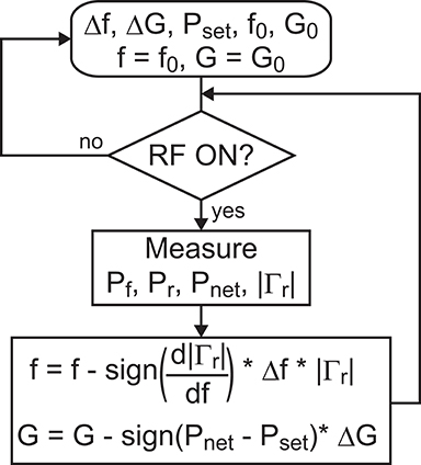
Figure 6. Flow chart of the automatic, fast, and autonomous control of the rf system. Δf, ΔG, Pset, f0, and G0 are the variation step of the frequency, the variation step of the gain of the VVA, the target value of the net rf power, the initial frequency, and the initial gain of the VVA, respectively.
Typical temporal evolutions of the frequency f, the reflection coefficient |Γr|, the optical emission intensity Iopt, the rf powers of Pf, Pr, and Pnet are shown in Figures 7, 8, where the initial frequency is set at f0 = 37.6 MHz in Figure 7 and 40.6 MHz in Figure 8, respectively. The target value of the net power is chosen as Pset = 40 W here, and the rf power is turned on for t = 0–100 ms for both cases. As can be seen in both figures, the reflection coefficient is rapidly decreased by automatic frequency tuning; then, plasma is produced and optical emission is detected. For the case of Figure 7, longer time is required to reduce the power reflection since the initial frequency for this case is more distant from the matching point than that in the case of Figure 8. However, stable plasma production can be obtained at about t ~ 10 ms. When choosing the initial frequency properly, stable plasma production can be obtained within a few of milliseconds as seen in Figure 8. Furthermore, it is demonstrated that the net power Pnet equal to the target value Pset is successfully sustained during the discharge, as seen in both Figures 7, 8, providing the fairly constant optical emission intensity Iopt. These data demonstrate that the automatic and fast control of the impedance and power tuning in the presently developed system can provide stable plasma production during pulse, which can provide high-speed minimization of power reflection.
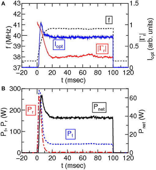
Figure 7. Temporal evolutions of (A) the rf frequency f, the optical emission intensity Iopt, and the reflection coefficient |Γr|, and (B) the rf powers Pf, Pr, and Pnet. The initial frequency and the target value of the net power are chosen as f0 = 37.6 MHz and Pset = 40 W, respectively.
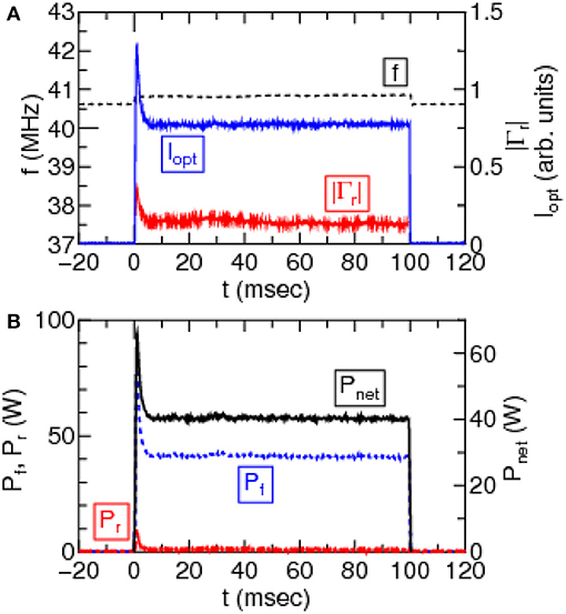
Figure 8. (A,B) The same data set as in Figures 7A,B for f0 = 40.6 MHz and Pset = 40 W.
One of the applications of the presently developed rf system is industrial plasma processing tool such as a plasma etcher operated in Bosch process, where etching and passivation gases are alternatively switched, e.g., as in Chang et al. [24]. Therefore, impedance tuning has to be finished for a much shorter time than the discharge pulse. Thus, high-speed impedance tuning would be an important technique to stably sustain the discharge when shortening the periods of each process. The plasma etcher utilizing the inductively coupled or helicon plasma source generally uses two rf amplifier for plasma production and substrate bias voltage [2, 25]. Moreover, the available space for the rf system in the recently proposed “Minimal Fab” (see “Introduction”) is significantly limited [12]. Therefore, the system having two rf generators has to be made compact to be fitted to the frame designed for Minimal Fab. Figure 9 shows the photograph of the presently developed rf system including the two rf amplifiers and the CompactRIO Single-Board Controller. It can be successfully made within the size of 220 mm in width, 135 mm in height, and 260 mm in depth and would be contained in the frame designed for Minimal Fab. The target value of the net power and the initial frequency can be set by putting the analog voltage signal, which can facilitate the initial test of the plasma source.
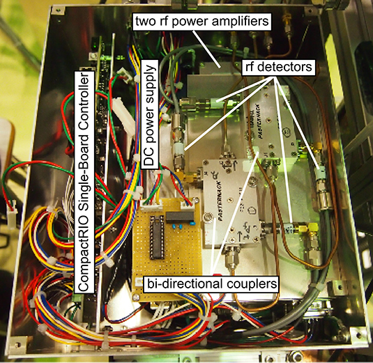
Figure 9. Photograph of the rf system containing the two rf generators, the CompactRIO Single-Board Controller, and the dc power supply. The total size is within 220 mm in width, 135 mm in height, and 260 mm in depth.
Conclusion
An automatic, fast, and autonomously controlled rf plasma source operational at variable frequency is developed. The rf system can be operated for the frequency range of 37–43 MHz, and the maximum rf power is about 200 W, where the impedance matching circuit consists of only the fixed ceramic capacitors, leading to a compact plasma source. Frequency tuning is accomplished within about 10 ms, and the net power corresponding to the forward power minus the reflected power is successfully maintained at a constant level during the pulse, which stabilizes the plasma source operation. For future application to the plasma etcher in Minimal Fab, the rf system containing the two rf generators is made compact, being contained within the size of 220 mm in width, 135 mm in height, and 260 mm in depth. The system will also be useful for space propulsion device utilizing the rf plasma source. The actual process of plasma etching and application to propulsion device remain further as challenging issues.
Data Availability Statement
All datasets generated for this study are included in the article/supplementary material.
Author Contributions
The rf generator was designed and assembled by KT. The controller program was written by KT. KH installed the generator to the plasma source designed and assembled by KT. The data were taken and analyzed by KT and KH. The results were discussed by KT, KH, and AA. KT wrote the manuscript. KH and AA reviewed the manuscript.
Funding
This work was partially supported by Strategic Core Technology Advancement Program (Supporting Industry Program) by Tohoku Bureau of Economy, Trade and Industry. This is also partially supported by a grant-in-aid for scientific research (18K18907, 18K18746, and 19H00663) from the Japan Society for the Promotion of Science and JAXA.
Conflict of Interest
The authors declare that the research was conducted in the absence of any commercial or financial relationships that could be construed as a potential conflict of interest.
References
1. Hopwood J. Review of inductively coupled plasmas for plasma processing. Plasma Sources Sci Technol. (1992) 1:109. doi: 10.1088/0963-0252/1/2/006
2. Donnelly VM, Kornblit A. Plasma etching: yesterday, today, and tomorrow. J Vac Sci Technol A. (2013) 31:050825. doi: 10.1116/1.4819316
3. Charles C. Plasmas for spacecraft propulsion. J Phys D Appl Phys. (2009) 42:163001. doi: 10.1088/0022-3727/42/16/163001
4. Takahashi K. Helicon-type radiofrequency plasma thrusters and magnetic plasma nozzles. Rev Mod Plasma Phys. (2019) 3:3. doi: 10.1007/s41614-019-0024-2
5. Kraus W, Schiesko L, Bonomo F, Fantz U, Heinemann B, Hurlbatt A, et al. First beam extraction experiments at BATMAN Upgrade. AIP Conf Proc. (2018) 2052:040004. doi: 10.1063/1.5083738
6. Olsen CS, Maxwell GB, Carter MD, Chang-Díaz FR, Giambusso M, Glover TW, et al. Investigation of plasma detachment from a magnetic nozzle in the plume of the VX-200 magnetoplasma thruster. IEEE Trans Plasma Sci. (2015) 43:252–68. doi: 10.1109/TPS.2014.2321257
7. Takahashi K, Charles C, Boswell RW. Approaching the theoretical limit of diamagnetic-induced momentum in a rapidly diverging magnetic nozzle. Phys Rev Lett. (2013) 110:195003. doi: 10.1103/PhysRevLett.110.195003
8. Takahashi K, Ando A. Laboratory observation of a plasma-flow-state transition from diverging to stretching a magnetic nozzle. Phys Rev Lett. (2017) 118:225002. doi: 10.1103/PhysRevLett.118.225002
9. Charles C, Boswell RW, Bish A. Low-weight fixed ceramic capacitor impedance matching system for an electrothermal plasma microthruster. J Propul Power. 30:1117–21. doi: 10.2514/1.B35119
10. Aanesland A, Rafalskyi D, Bredin J, Grondein P, Oudini N, Chabert P, et al. The PEGASES gridded ion–ion thruster performance and predictions. IEEE Trans Plasma Sci. (2015) 43:321–6. doi: 10.1109/TPS.2014.2369534
11. Goebel DM. Analytical discharge model for RF ion thrusters. IEEE Trans Plasma Sci. (2008) 36:2111–21. doi: 10.1109/TPS.2008.2004232
12. Khumpuang S, Hara S. A MOSFET fabrication using a maskless lithography system in clean-localized environment of Minimal Fab. IEEE Trans Semicond Manuf. (2015) 28:393–8. doi: 10.1109/TSM.2015.2429572
13. Khumpuang S, Imura F, Hara S. Analyses on cleanroom-free performance and transistor manufacturing cycle time of Minimal Fab. IEEE Trans Semicond Manuf. (2015) 28:551–6. doi: 10.1109/TSM.2015.2487324
14. Tanaka H, Ogiso H, Nakano S, Hayami T, Miyazaki T, Khumpuang S, et al. Scallop reduction in Bosch process using a small chamber and rapid gas switching rate. IEEJ Trans Sens Micromach. (2016) 136:499–504. doi: 10.1541/ieejsmas.136.499
15. Charles C, Boswell RW, Bish A. Variable frequency matching to a radiofrequency source immersed in vacuum. J Phys D Appl Phys. (2013) 46:365203. doi: 10.1088/0022-3727/46/36/365203
16. Takahashi K, Nakano Y, Ando A. Frequency-tuning radiofrequency plasma source operated in inductively-coupled mode under a low magnetic field. J Phys D Appl Phys. (2017) 50:265201. doi: 10.1088/1361-6463/aa7524
17. Fujita H, Akagi H, Shinohara S. A 2-MHz 6-kVA voltage-source inverter using low-profile MOSFET modules for low-temperature plasma generators. IEEE Trans Power Electronics. (1999) 14:1014–20. doi: 10.1109/63.803394
18. Ando A, Komuro A, Matsuno T, Tsumori K, Takeiri Y. Radio frequency ion source operated with field effect transistor based radio frequency system. Rev Sci Instrum. (2010) 81:02B107. doi: 10.1063/1.3279306
19. Takahashi K, Ando A. Observation of stationary plasma striation and collimated plasma transport in a 100-kHz inductively coupled plasma discharge. IEEE Trans Plasma Sci. (2014) 42:2784–5. doi: 10.1109/TPS.2014.2308893
20. Charles C, Liang W, Raymond L, Rivas-Davila J, Boswell RW. Vacuum testing of a miniaturized switch mode amplifier powering an electrothermal plasma micro-thruster. Front Phys. (2017) 5:36. doi: 10.3389/fphy.2017.00036
21. Lieberman MA, Lichtenberg AJ. Principles of plasma discharges and material processing. 2nd edn. Hoboken, NJ: John Wiley & Sons, Inc (2005). doi: 10.1002/0471724254
22. Godyak VA, Piejak RB, Alexandrovich BM. Experimental setup and electrical characteristics of an inductively coupled plasma. J Appl Phys. (1999) 85:703–12. doi: 10.1063/1.369150
24. Chang C, Wang YF, Kanamori Y, Shih JJ, Kawai Y, Lee CK, et al. Etching submicrometer trenches by using the Bosch process and its application to the fabrication of antireflection structures. J Micromech Microeng. (2005) 15:580. doi: 10.1088/0960-1317/15/3/020
Keywords: rf plasma source, impedance matching, rf generator, low-pressure plasma, compact plasma source
Citation: Takahashi K, Hanaoka K and Ando A (2020) Fast and Automatic Control of a Frequency-Tuned Radiofrequency Plasma Source. Front. Phys. 7:227. doi: 10.3389/fphy.2019.00227
Received: 15 October 2019; Accepted: 10 December 2019;
Published: 23 January 2020.
Edited by:
Agnes Granier, Centre National de la Recherche Scientifique (CNRS), FranceReviewed by:
Alan A. Howling, École Polytechnique Fédérale de Lausanne, SwitzerlandSaikat Chakraborty Thakur, University of California, San Diego, United States
Copyright © 2020 Takahashi, Hanaoka and Ando. This is an open-access article distributed under the terms of the Creative Commons Attribution License (CC BY). The use, distribution or reproduction in other forums is permitted, provided the original author(s) and the copyright owner(s) are credited and that the original publication in this journal is cited, in accordance with accepted academic practice. No use, distribution or reproduction is permitted which does not comply with these terms.
*Correspondence: Kazunori Takahashi, a2F6dW5vcmlAZWNlaS50b2hva3UuYWMuanA=